EP1565929B1 - Verfahren zur plasmabehandlung von oberflächen im vakuum - Google Patents
Verfahren zur plasmabehandlung von oberflächen im vakuum Download PDFInfo
- Publication number
- EP1565929B1 EP1565929B1 EP03769144A EP03769144A EP1565929B1 EP 1565929 B1 EP1565929 B1 EP 1565929B1 EP 03769144 A EP03769144 A EP 03769144A EP 03769144 A EP03769144 A EP 03769144A EP 1565929 B1 EP1565929 B1 EP 1565929B1
- Authority
- EP
- European Patent Office
- Prior art keywords
- substrate
- treatment
- distribution
- plasma
- movement
- Prior art date
- Legal status (The legal status is an assumption and is not a legal conclusion. Google has not performed a legal analysis and makes no representation as to the accuracy of the status listed.)
- Expired - Lifetime
Links
Images


Classifications
-
- H—ELECTRICITY
- H01—ELECTRIC ELEMENTS
- H01J—ELECTRIC DISCHARGE TUBES OR DISCHARGE LAMPS
- H01J37/00—Discharge tubes with provision for introducing objects or material to be exposed to the discharge, e.g. for the purpose of examination or processing thereof
- H01J37/32—Gas-filled discharge tubes
- H01J37/34—Gas-filled discharge tubes operating with cathodic sputtering
- H01J37/3411—Constructional aspects of the reactor
- H01J37/345—Magnet arrangements in particular for cathodic sputtering apparatus
- H01J37/3455—Movable magnets
-
- C—CHEMISTRY; METALLURGY
- C23—COATING METALLIC MATERIAL; COATING MATERIAL WITH METALLIC MATERIAL; CHEMICAL SURFACE TREATMENT; DIFFUSION TREATMENT OF METALLIC MATERIAL; COATING BY VACUUM EVAPORATION, BY SPUTTERING, BY ION IMPLANTATION OR BY CHEMICAL VAPOUR DEPOSITION, IN GENERAL; INHIBITING CORROSION OF METALLIC MATERIAL OR INCRUSTATION IN GENERAL
- C23C—COATING METALLIC MATERIAL; COATING MATERIAL WITH METALLIC MATERIAL; SURFACE TREATMENT OF METALLIC MATERIAL BY DIFFUSION INTO THE SURFACE, BY CHEMICAL CONVERSION OR SUBSTITUTION; COATING BY VACUUM EVAPORATION, BY SPUTTERING, BY ION IMPLANTATION OR BY CHEMICAL VAPOUR DEPOSITION, IN GENERAL
- C23C14/00—Coating by vacuum evaporation, by sputtering or by ion implantation of the coating forming material
- C23C14/22—Coating by vacuum evaporation, by sputtering or by ion implantation of the coating forming material characterised by the process of coating
- C23C14/34—Sputtering
- C23C14/35—Sputtering by application of a magnetic field, e.g. magnetron sputtering
-
- C—CHEMISTRY; METALLURGY
- C23—COATING METALLIC MATERIAL; COATING MATERIAL WITH METALLIC MATERIAL; CHEMICAL SURFACE TREATMENT; DIFFUSION TREATMENT OF METALLIC MATERIAL; COATING BY VACUUM EVAPORATION, BY SPUTTERING, BY ION IMPLANTATION OR BY CHEMICAL VAPOUR DEPOSITION, IN GENERAL; INHIBITING CORROSION OF METALLIC MATERIAL OR INCRUSTATION IN GENERAL
- C23C—COATING METALLIC MATERIAL; COATING MATERIAL WITH METALLIC MATERIAL; SURFACE TREATMENT OF METALLIC MATERIAL BY DIFFUSION INTO THE SURFACE, BY CHEMICAL CONVERSION OR SUBSTITUTION; COATING BY VACUUM EVAPORATION, BY SPUTTERING, BY ION IMPLANTATION OR BY CHEMICAL VAPOUR DEPOSITION, IN GENERAL
- C23C14/00—Coating by vacuum evaporation, by sputtering or by ion implantation of the coating forming material
- C23C14/22—Coating by vacuum evaporation, by sputtering or by ion implantation of the coating forming material characterised by the process of coating
- C23C14/34—Sputtering
- C23C14/3407—Cathode assembly for sputtering apparatus, e.g. Target
-
- C—CHEMISTRY; METALLURGY
- C23—COATING METALLIC MATERIAL; COATING MATERIAL WITH METALLIC MATERIAL; CHEMICAL SURFACE TREATMENT; DIFFUSION TREATMENT OF METALLIC MATERIAL; COATING BY VACUUM EVAPORATION, BY SPUTTERING, BY ION IMPLANTATION OR BY CHEMICAL VAPOUR DEPOSITION, IN GENERAL; INHIBITING CORROSION OF METALLIC MATERIAL OR INCRUSTATION IN GENERAL
- C23C—COATING METALLIC MATERIAL; COATING MATERIAL WITH METALLIC MATERIAL; SURFACE TREATMENT OF METALLIC MATERIAL BY DIFFUSION INTO THE SURFACE, BY CHEMICAL CONVERSION OR SUBSTITUTION; COATING BY VACUUM EVAPORATION, BY SPUTTERING, BY ION IMPLANTATION OR BY CHEMICAL VAPOUR DEPOSITION, IN GENERAL
- C23C14/00—Coating by vacuum evaporation, by sputtering or by ion implantation of the coating forming material
- C23C14/22—Coating by vacuum evaporation, by sputtering or by ion implantation of the coating forming material characterised by the process of coating
- C23C14/54—Controlling or regulating the coating process
- C23C14/542—Controlling the film thickness or evaporation rate
-
- C—CHEMISTRY; METALLURGY
- C23—COATING METALLIC MATERIAL; COATING MATERIAL WITH METALLIC MATERIAL; CHEMICAL SURFACE TREATMENT; DIFFUSION TREATMENT OF METALLIC MATERIAL; COATING BY VACUUM EVAPORATION, BY SPUTTERING, BY ION IMPLANTATION OR BY CHEMICAL VAPOUR DEPOSITION, IN GENERAL; INHIBITING CORROSION OF METALLIC MATERIAL OR INCRUSTATION IN GENERAL
- C23C—COATING METALLIC MATERIAL; COATING MATERIAL WITH METALLIC MATERIAL; SURFACE TREATMENT OF METALLIC MATERIAL BY DIFFUSION INTO THE SURFACE, BY CHEMICAL CONVERSION OR SUBSTITUTION; COATING BY VACUUM EVAPORATION, BY SPUTTERING, BY ION IMPLANTATION OR BY CHEMICAL VAPOUR DEPOSITION, IN GENERAL
- C23C16/00—Chemical coating by decomposition of gaseous compounds, without leaving reaction products of surface material in the coating, i.e. chemical vapour deposition [CVD] processes
- C23C16/44—Chemical coating by decomposition of gaseous compounds, without leaving reaction products of surface material in the coating, i.e. chemical vapour deposition [CVD] processes characterised by the method of coating
- C23C16/50—Chemical coating by decomposition of gaseous compounds, without leaving reaction products of surface material in the coating, i.e. chemical vapour deposition [CVD] processes characterised by the method of coating using electric discharges
-
- C—CHEMISTRY; METALLURGY
- C23—COATING METALLIC MATERIAL; COATING MATERIAL WITH METALLIC MATERIAL; CHEMICAL SURFACE TREATMENT; DIFFUSION TREATMENT OF METALLIC MATERIAL; COATING BY VACUUM EVAPORATION, BY SPUTTERING, BY ION IMPLANTATION OR BY CHEMICAL VAPOUR DEPOSITION, IN GENERAL; INHIBITING CORROSION OF METALLIC MATERIAL OR INCRUSTATION IN GENERAL
- C23C—COATING METALLIC MATERIAL; COATING MATERIAL WITH METALLIC MATERIAL; SURFACE TREATMENT OF METALLIC MATERIAL BY DIFFUSION INTO THE SURFACE, BY CHEMICAL CONVERSION OR SUBSTITUTION; COATING BY VACUUM EVAPORATION, BY SPUTTERING, BY ION IMPLANTATION OR BY CHEMICAL VAPOUR DEPOSITION, IN GENERAL
- C23C16/00—Chemical coating by decomposition of gaseous compounds, without leaving reaction products of surface material in the coating, i.e. chemical vapour deposition [CVD] processes
- C23C16/44—Chemical coating by decomposition of gaseous compounds, without leaving reaction products of surface material in the coating, i.e. chemical vapour deposition [CVD] processes characterised by the method of coating
- C23C16/52—Controlling or regulating the coating process
Definitions
- the present invention is based on needs which have arisen in magnetron sputter coating of substrates. However, it has been found that the solution found according to the present invention can generally be used for substrate surfaces treated by vacuum treatment processes.
- each of the release processes and, according to the coating processes of the individual materials is considered as a vacuum treatment process per se. In such a case, two or more treatment processes are performed simultaneously.
- the solution found according to the present invention results from the process according to claim 1.
- the predefined relative movement and the predetermined temporal change are each created periodically and their dependency is established by synchronization. It is to point out that it is generally not necessary to form the periodicities created in the same way.
- the periods of the mentioned temporal change and the mentioned relative movement may be quite different, both in such a way that one period is an integer multiple of the others or in such a way that the periods are in a non-integer relationship to each other.
- the treatment result is a coating of the mentioned surfaces.
- the treatment result can also be etching of the treatment surface, both coating or etching, reactive or non-reactive.
- the creation of the predetermined movement is created by a predetermined movement of the inhomogeneous density distribution with respect to the vacuum recipient.
- the plasma discharge is created with at least one region with an outstanding density maximum.
- the inhomogeneous density distribution is at least co-generated by means of a magnetic field.
- a simple possibility is created to realize the relative movement of the inhomogeneous plasma density distribution, namely the fact that the magnetic field distribution, also inhomogeneous, in the recipient, wherein the discharge is created, is moved.
- the plasma discharge is generated by means of DC, AC, DC and superimposed AC or by means of Hf.
- the substrate may optionally be biased by means of DC, AC, DC and superimposed AC or Hf, and then, preferably in addition to the variation of the electrical signal operating the plasma discharge, this bias signal is temporally changed in a predetermined manner. If we speak in the present context of a temporal change of an AC signal, then its angle or amplitude change, so its modulation is addressed.
- the vacuum treatment process is designed as a magnetron sputtering process, and the predetermined relative movement is realized at least also by a predetermined movement of the magnetron tunneling field with respect to a target sputtering surface.
- magnetron sputtering is excellently suited to proceed according to the present method, because there are already the means to move an inhomogeneous plasma density distribution with respect to a substrate.
- the relative movement of the locally inhomogeneous density distribution of the plasma relative to the substrate is realized by the mechanical movement of a magnetic field generating arrangement outside and / or inside the vacuum recipient.
- Such arrangements are realized, e.g. with electromagnets, coil arrangements, e.g. Helmholtz coils, deflection coils, in magnetrons with magnet arrangements under the target which rotate or in given x and y movements, linearly and in mutual dependence, are moved.
- the magnetic field can also be moved electrically, by controlled, time-variable control of permanently installed coil arrangements.
- Mechanical movement of magnetic field generators and electrical, time-variable control of coils, which can also be moved mechanically, can certainly be combined.
- a solid is released into the treatment atmosphere with the aid of the discharge. It is further admitted into the said atmosphere, a reactive gas.
- the distribution of the compound ratio between solid and components of the reactive gas on the surface is set as a treatment result.
- a treatment intermediate result is measured, compared with a desired treatment intermediate result, and the predetermined relative movement and / or the temporal change are adjusted as a function of the comparison result.
- the measurement mentioned more preferably, without vacuum interruption.
- the substrate can very well be transported from one vacuum to another, for example, from the treatment atmosphere into a measurement atmosphere, or the measurement mentioned, as more preferably, is carried out in situ during the substrate treatment, ie in the treatment process atmosphere.
- the measurement result is supplied as a measured controlled variable to a control loop, which sets the predetermined relative movement and / or temporal change as a manipulated variable for a treatment result control.
- the proposed method is particularly suitable for the production of surface acoustic wave based or on the basis of "bulk acoustic waves" working components.
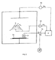
- a plasma discharge gap 5 is provided, as schematically shown with an electrode 5a and an electrode 5b.
- the plasma discharge path 5 is electrically operated by means of a generator 7, which may be a DC, an AC, a DC + AC or a Hf generator.
- a generator 7 which may be a DC, an AC, a DC + AC or a Hf generator.
- the electrodes 5a, 5b as known in the art, designed.
- the generator 7 depending on the purpose of electrically floating, be placed on ground potential or other reference potential ⁇ 2 , which of course may be equal to ⁇ 1 .
- the generator 7 has a modulation input 7 MOD what basically the route 5 supplying electric signal E can be modulated in time 5 relative to DC-value and / or phase and / or amplitude and / or time.
- the plasma discharge path 5 is designed such that it generates an inhomogeneously density-distributed plasma.
- a two-dimensional inhomogeneous plasma density distribution is shown in FIG. 1 at ⁇ PL , for example with a density maximum M.
- the plasma density distribution ⁇ PL can be moved with respect to a substrate 9 with a predetermined movement.
- FIG. 1 illustrates the possibility of realizing this by means of a magnetic field.
- This is done locally in the plasma a magnetic field H generated, for example, with a controlled moving coil assembly.
- the magnetic field distribution in the discharge path 5 is moved by mechanical movement of the coil arrangement L, as schematized by a motor drive 13 in FIG.
- the movement imposed by the drive 13 of the coil arrangement L is predefined at control inputs 13 SX , 13 SY , in the x and y direction, of the drive 13.
- the inhomogeneous density distribution ⁇ PL of the plasma of a predetermined movement is imposed, which is done according to FIG. 1 by corresponding predetermined movement of a magnetic field distribution in the plasma zone 5.
- the substrate carrier or the substrate 9 can be biased by means of a signal generator 15, again in principle DC, AC, AC + DC or Hf.
- a signal generator 15 again in principle DC, AC, AC + DC or Hf.
- the generator 15 preferably also has a modulation input 15 MOD, is what the bias signal, as already has been explained 5 for operation of the plasma discharge path 5 with respect to the signal E, modulated in time or changed.
- E 5 , B or E 9 , B are periodic signals, 13 S or 5 MOD , 13 S , are set, corresponding to 7 MOD , in addition to the respective amplitudes, the temporal signal curves (pulse, trapezoid, triangle, sine etc.), it also set the signal period or frequency.
- the relative movement of the inhomogeneous plasma density distribution ⁇ PL with respect to the substrate surface to be treated can be effected by displacement or movement of the plasma density distribution ⁇ PL with respect to the recipient 1. It is essential that, viewed over the treatment time, and after a settable with the mentioned movement pattern, the substrate surface sequentially the inhomogeneous plasma density distribution ⁇ PL is swept over. At the same time, as mentioned, the variation of the discharge voltage or of the discharge current and / or, if provided, the bias voltage on the substrate over time.
- FIG. 2 is still highly schematic, a circular disk-shaped substrate 19 on a substrate support 21 in plan view.
- a process chamber according to FIG. 1 of FIG. 1 is not shown in this illustration.
- a plasma discharge PL with a substantially two-dimensionally inhomogeneous plasma density distribution ⁇ PL is stationarily formed in the vacuum recipient, as shown in FIG. 2.
- the substrate 19 is displaced relative to the chamber-stationary, inhomogeneous density distribution ⁇ PL .
- the control signal 13 sx With the control signal 13 sx , the x movement of the substrate carrier, with the control signal 13 sy the y movement is controlled.
- the curves of the movement B (x, y) as well as of E S and E 9 are shown.
- the mutual phase position is set, such as the phase angle ⁇ xy between movement in the x direction and movement in the y direction, and the phase position between E 5 and, for example, B x , ⁇ EB .
- the phase shift ⁇ xy , ⁇ EB set and the signals are synchronized in the sense of a phase lock.
- the time courses of the respective signals, as shown in FIG. 3 on the course of B x at (a) are set.
- the surface distribution of the processing result is adjusted according to the invention on the plasma-treated substrate surface.
- etching profiles can be set on the substrate surface, non-reactive or reactive etching processes.
- PECVD plasma-assisted chemical vapor deposition
- the surface profile of the layers deposited on the substrate surface considered can also be adjusted with the illustrated procedure. If a constant reactive gas partial pressure over the substrate surface is set in reactive processes, or also in the PEVCD process, the illustrated procedure makes it possible to design the resulting planar distribution of the deposited layer in a targeted manner with regard to layer thickness or stoichiometric ratios.
- magnetron sputtering Pronounced inhomogeneous plasma density distributions are used in magnetron sputtering, where regions of high plasma densities are created over the target sputtering surfaces along the tunnel-shaped magnetic field loops.
- magnetron sputtering is ideally suited to be used according to the inventive method.
- the magnetron discharge can be operated with DC, with AC, with superimposed AC + DC or with Hf. It may also be reactive magnetron sputtering or non-reactive magnetron sputtering.
- the present invention has also been developed to meet requirements resulting from the magnetron sputter coating technique and, as explained with reference to FIGS. 1-3, quite fundamentally to the setting of the effect or result distribution of a plasma treatment along a substrate surface extended.
- FIG. 4 shows a vacuum treatment chamber in the form of a magnetron sputter coating chamber, to which the production method according to the invention is carried out.
- a vacuum chamber 30 can be evacuated via a pump device 32.
- On a Tarruckückplatte 44 is a target 33rd made of material to be sputtered.
- Behind the Tartet Wegplatte 44, outside the vacuum chamber 30, are a magnet system 35. This includes, for example, a rotatably driven about a central axis
- a magnet carrier plate 36 with respect thereto asymmetrically arranged in plan view, for example, kidney-shaped - it is referenced to FIG.
- the magnets 40 of the magnet assembly may be driven and, as shown at R, may also be radially driven, in addition to its rotational movement ⁇ about axis A.
- the magnet arrangement 40 as shown schematically at H, a decidedly inhomogeneous magnetic field with respect to the substrate 45 is moved on the substrate carrier 43.
- the rotational movement of the magnet arrangement 35 is scanned by means of a detector arrangement 37.
- the sampling pulses I of the detector unit 37 are time-delayed adjustable on a unit 41, ⁇ ; the output-side, time-delayed pulses I ( ⁇ ) trigger or synchronize the eg sinusoidal signal E 5 .
- a further control input at the generator 38, 38 S the stroke of the sinusoidal signal component of E 5 is set.
- a gas line for a working gas preferably argon
- a reactive gas is admitted into the process space for reactive Magnetronsputterbe Anlagenen.
- the distribution of the composition of the layer can be adjusted by adjusting the movement of the inhomogeneously densely distributed magnetron plasma and the temporal guidance of the plasma discharge power E 5 along the substrate surface the layer thickness distribution.
- the distribution of the treatment result at the surface of the substrate 54 recorded.
- the measurement result x is compared with a predefined result distribution W, at a difference unit 56.
- the comparison of the result distribution currently determined by measurement takes place with a desired distribution, which is two-dimensionally decisive for the treatment time already carried out.
- Deviations between actual (X) and desired (W) distribution are supplied via a computing unit R as actuating signals 58 s to a generator unit 58 for the plasma discharge and / or to a guide unit 60 for the movement of the inhomogeneous plasma density distribution ⁇ PL with respect to the substrate surface.
- actuating signals 58 s to a generator unit 58 for the plasma discharge and / or to a guide unit 60 for the movement of the inhomogeneous plasma density distribution ⁇ PL with respect to the substrate surface.
- FIG. 6 shows, in plan view, the magnet system of the magnetron arrangement driven at a constant rotational speed .omega.
- FIG. 7 shows on the 6 "substrate the area distribution of the treatment result, namely the reactive magnetron sputter coating with the AlN layer, as a reference example without modulation of the discharge power E 5 .
- FIG. 8 shows the result.
- the layer thickness distribution according to FIG. 9 also resulted from a modulation stroke of the discharge power E 5 of 5.6% with a locked phase ⁇ EB of 90 °.
- a main application of the present invention is shown schematically from a slightly different perspective than heretofore.
- one of the distributions of a treatment result achieved according to the invention is the distribution of a layer thickness.
- a layer is deposited on the surface T of a planar substrate according to the method according to the invention, with the surface S and the distribution of the thickness d along the surface T. If the coordinate surface x T / in the plane surface T of the substrate is y T and Z T placed, at the location x O / y o so the Z-axis has the direction of the surface normal N T at said location.
- the surface normal N S is now at the layer surface S according to the invention at the same location x o / y o spatially with respect to the direction of the surface normal N T tilted, according to the coordinate system in the surface S at the location x o / y o .
- This tilting of the layer surface S with respect to the substantially planar substrate surface T or, more generally, a nonplanar surface T is referred to as layer tilting.
- An essential application of the present invention is to interpret the Schichtverkippung spatially according to a predetermined ratio, and possibly along the substrate surface T locally different.
- the layer tilt, which is aimed at according to the invention can be zero at least in regions of the surface T, then the direction N S coincides with the direction N T.
Landscapes
- Chemical & Material Sciences (AREA)
- Engineering & Computer Science (AREA)
- Chemical Kinetics & Catalysis (AREA)
- Materials Engineering (AREA)
- Mechanical Engineering (AREA)
- Metallurgy (AREA)
- Organic Chemistry (AREA)
- Physics & Mathematics (AREA)
- General Chemical & Material Sciences (AREA)
- Plasma & Fusion (AREA)
- Analytical Chemistry (AREA)
- Physical Vapour Deposition (AREA)
- Treatments Of Macromolecular Shaped Articles (AREA)
- Plasma Technology (AREA)
- Chemical Vapour Deposition (AREA)
- Physical Or Chemical Processes And Apparatus (AREA)
- Drying Of Semiconductors (AREA)
Applications Claiming Priority (3)
| Application Number | Priority Date | Filing Date | Title |
|---|---|---|---|
| CH201902 | 2002-11-29 | ||
| CH20192002 | 2002-11-29 | ||
| PCT/CH2003/000744 WO2004050943A2 (de) | 2002-11-29 | 2003-11-13 | Verfahren zur plasmabehandlung von oberflächen in vakumm und anlage hierfür |
Publications (2)
| Publication Number | Publication Date |
|---|---|
| EP1565929A2 EP1565929A2 (de) | 2005-08-24 |
| EP1565929B1 true EP1565929B1 (de) | 2007-10-10 |
Family
ID=32399969
Family Applications (1)
| Application Number | Title | Priority Date | Filing Date |
|---|---|---|---|
| EP03769144A Expired - Lifetime EP1565929B1 (de) | 2002-11-29 | 2003-11-13 | Verfahren zur plasmabehandlung von oberflächen im vakuum |
Country Status (10)
| Country | Link |
|---|---|
| US (2) | US7138343B2 (https=) |
| EP (1) | EP1565929B1 (https=) |
| JP (1) | JP4741241B2 (https=) |
| KR (1) | KR101177127B1 (https=) |
| CN (1) | CN1745453B (https=) |
| AT (1) | ATE375600T1 (https=) |
| AU (1) | AU2003277791A1 (https=) |
| DE (1) | DE50308371D1 (https=) |
| TW (1) | TWI325149B (https=) |
| WO (1) | WO2004050943A2 (https=) |
Families Citing this family (8)
| Publication number | Priority date | Publication date | Assignee | Title |
|---|---|---|---|---|
| US7264850B1 (en) * | 1992-12-28 | 2007-09-04 | Semiconductor Energy Laboratory Co., Ltd. | Process for treating a substrate with a plasma |
| KR101177127B1 (ko) * | 2002-11-29 | 2012-08-24 | 오씨 외를리콘 발처스 악티엔게젤샤프트 | 기판의 제조 방법 및 이를 위한 장치 |
| DE102006036403B4 (de) * | 2006-08-02 | 2009-11-19 | Von Ardenne Anlagentechnik Gmbh | Verfahren zur Beschichtung eines Substrats mit einer definierten Schichtdickenverteilung |
| US20090078199A1 (en) * | 2007-09-21 | 2009-03-26 | Innovation Vacuum Technology Co., Ltd. | Plasma enhanced chemical vapor deposition apparatus |
| EP2223328B1 (en) * | 2007-12-07 | 2017-06-21 | Evatec AG | Method of magnetron sputtering |
| CN103094048B (zh) * | 2011-11-01 | 2015-08-19 | 凌嘉科技股份有限公司 | 可位移调整磁控管的装置 |
| US20170040140A1 (en) * | 2015-08-06 | 2017-02-09 | Seagate Technology Llc | Magnet array for plasma-enhanced chemical vapor deposition |
| DE102018213534A1 (de) * | 2018-08-10 | 2020-02-13 | Fraunhofer-Gesellschaft zur Förderung der angewandten Forschung e.V. | Vorrichtung und Verfahren zur Herstellung von Schichten mit verbesserter Uniformität bei Beschichtungsanlagen mit horizontal rotierender Substratführung |
Family Cites Families (22)
| Publication number | Priority date | Publication date | Assignee | Title |
|---|---|---|---|---|
| JPS59175125A (ja) * | 1983-03-24 | 1984-10-03 | Toshiba Corp | ドライエツチング装置 |
| US4668365A (en) * | 1984-10-25 | 1987-05-26 | Applied Materials, Inc. | Apparatus and method for magnetron-enhanced plasma-assisted chemical vapor deposition |
| US4858556A (en) * | 1986-09-15 | 1989-08-22 | Siebert Jerome F | Method and apparatus for physical vapor deposition of thin films |
| JPH0629249A (ja) * | 1991-10-08 | 1994-02-04 | Ulvac Japan Ltd | プラズマエッチング装置 |
| JP3362432B2 (ja) * | 1992-10-31 | 2003-01-07 | ソニー株式会社 | プラズマ処理方法及びプラズマ処理装置 |
| US5500077A (en) * | 1993-03-10 | 1996-03-19 | Sumitomo Electric Industries, Ltd. | Method of polishing/flattening diamond |
| JP3250768B2 (ja) * | 1993-09-28 | 2002-01-28 | アルプス電気株式会社 | ダイヤモンド状炭素膜の形成方法、磁気ヘッドの製造方法および磁気ディスクの製造方法 |
| US5529671A (en) * | 1994-07-27 | 1996-06-25 | Litton Systems, Inc. | Apparatus and method for ion beam polishing and for in-situ ellipsometric deposition of ion beam films |
| US5945008A (en) * | 1994-09-29 | 1999-08-31 | Sony Corporation | Method and apparatus for plasma control |
| JPH09256149A (ja) * | 1996-03-22 | 1997-09-30 | Tokyo Electron Ltd | スパッタリング装置およびスパッタリング方法 |
| JP3744089B2 (ja) * | 1996-12-02 | 2006-02-08 | 富士電機ホールディングス株式会社 | マグネトロンスパッタ成膜装置および成膜方法 |
| JPH11176815A (ja) * | 1997-12-15 | 1999-07-02 | Ricoh Co Ltd | ドライエッチングの終点判定方法およびドライエッチング装置 |
| US6290825B1 (en) * | 1999-02-12 | 2001-09-18 | Applied Materials, Inc. | High-density plasma source for ionized metal deposition |
| US6254745B1 (en) * | 1999-02-19 | 2001-07-03 | Tokyo Electron Limited | Ionized physical vapor deposition method and apparatus with magnetic bucket and concentric plasma and material source |
| US6312568B2 (en) * | 1999-12-07 | 2001-11-06 | Applied Materials, Inc. | Two-step AIN-PVD for improved film properties |
| US6767475B2 (en) * | 2000-05-25 | 2004-07-27 | Atomic Telecom | Chemical-organic planarization process for atomically smooth interfaces |
| US6413382B1 (en) * | 2000-11-03 | 2002-07-02 | Applied Materials, Inc. | Pulsed sputtering with a small rotating magnetron |
| EP1254970A1 (de) * | 2001-05-03 | 2002-11-06 | Unaxis Balzers Aktiengesellschaft | Magnetronsputterquelle mit mehrteiligem Target |
| SE525231C2 (sv) * | 2001-06-14 | 2005-01-11 | Chemfilt R & D Ab | Förfarande och anordning för att alstra plasma |
| US20030164998A1 (en) * | 2002-03-01 | 2003-09-04 | The Regents Of The University Of California | Ion-assisted deposition techniques for the planarization of topological defects |
| JP4728644B2 (ja) * | 2002-10-15 | 2011-07-20 | エリコン・トレーディング・アクチェンゲゼルシャフト,トリュープバッハ | マグネトロンスパッタ成膜基板の製造方法およびその装置 |
| KR101177127B1 (ko) * | 2002-11-29 | 2012-08-24 | 오씨 외를리콘 발처스 악티엔게젤샤프트 | 기판의 제조 방법 및 이를 위한 장치 |
-
2003
- 2003-11-13 KR KR1020057009745A patent/KR101177127B1/ko not_active Expired - Fee Related
- 2003-11-13 CN CN2003801093200A patent/CN1745453B/zh not_active Expired - Fee Related
- 2003-11-13 DE DE50308371T patent/DE50308371D1/de not_active Expired - Lifetime
- 2003-11-13 AT AT03769144T patent/ATE375600T1/de not_active IP Right Cessation
- 2003-11-13 WO PCT/CH2003/000744 patent/WO2004050943A2/de not_active Ceased
- 2003-11-13 JP JP2004555942A patent/JP4741241B2/ja not_active Expired - Fee Related
- 2003-11-13 US US10/536,204 patent/US7138343B2/en not_active Expired - Lifetime
- 2003-11-13 AU AU2003277791A patent/AU2003277791A1/en not_active Abandoned
- 2003-11-13 EP EP03769144A patent/EP1565929B1/de not_active Expired - Lifetime
- 2003-11-27 TW TW092133325A patent/TWI325149B/zh not_active IP Right Cessation
-
2006
- 2006-10-06 US US11/539,218 patent/US7429543B2/en not_active Expired - Lifetime
Also Published As
| Publication number | Publication date |
|---|---|
| TW200415687A (en) | 2004-08-16 |
| TWI325149B (en) | 2010-05-21 |
| CN1745453A (zh) | 2006-03-08 |
| AU2003277791A1 (en) | 2004-06-23 |
| WO2004050943A2 (de) | 2004-06-17 |
| WO2004050943A3 (de) | 2004-08-26 |
| EP1565929A2 (de) | 2005-08-24 |
| CN1745453B (zh) | 2011-08-31 |
| US7138343B2 (en) | 2006-11-21 |
| JP2006508242A (ja) | 2006-03-09 |
| AU2003277791A8 (en) | 2004-06-23 |
| US20060054493A1 (en) | 2006-03-16 |
| ATE375600T1 (de) | 2007-10-15 |
| US7429543B2 (en) | 2008-09-30 |
| DE50308371D1 (de) | 2007-11-22 |
| KR20050085214A (ko) | 2005-08-29 |
| US20070084715A1 (en) | 2007-04-19 |
| KR101177127B1 (ko) | 2012-08-24 |
| JP4741241B2 (ja) | 2011-08-03 |
Similar Documents
| Publication | Publication Date | Title |
|---|---|---|
| DE4029270C1 (https=) | ||
| EP1908091B1 (de) | Verfahren und vorrichtung zur mehrkathoden-pvd-beschichtung und substrat mit pvd-beschichtung | |
| DE69226322T2 (de) | Zerstäubungsanlage | |
| DE10018143A1 (de) | DLC-Schichtsystem sowie Verfahren und Vorrichtung zur Herstellung eines derartigen Schichtsystems | |
| WO2016156496A1 (de) | Verfahren zur herstellung von beschichteten substraten | |
| EP1565929B1 (de) | Verfahren zur plasmabehandlung von oberflächen im vakuum | |
| EP2165003A1 (de) | Pdv-verfahren und pvd-vorrichtung zur erzeugung von reibungsarmen, verschleissbeständigen funktionsschichten und damit hergestellte beschichtungen | |
| EP2013374A2 (de) | Vorrichtung und verfahren zur homogenen pvd-beschichtung | |
| WO1999014390A2 (de) | Verfahren zur sputterbeschichtung von oberflächen | |
| WO2001063643A1 (de) | Verfahren zur steuerung der plasmadichte oder deren verteilung | |
| JP5108177B2 (ja) | 真空処理装置および工作物の製造方法 | |
| Zdunek et al. | Optimization of gas injection conditions during deposition of AlN layers by novel reactive GIMS method | |
| EP2175044B1 (de) | PVD-Beschichtungsverfahren, Vorrichtung zur Durchführung des Verfahrens und nach dem Verfahren beschichtete Substanzen | |
| DE102016116762A1 (de) | Verfahren zum Abscheiden einer Schicht mittels einer Magnetronsputtereinrichtung | |
| DE10145201C1 (de) | Einrichtung zum Beschichten von Substraten mit gekrümmter Oberfläche durch Pulsmagnetron-Zerstäuben | |
| EP4476758B1 (de) | Symmetrischer prozessreaktor | |
| Sano et al. | Titanium nitride coating on implanted layer using titanium plasma based ion implantation | |
| KR20140110186A (ko) | 압축잔류응력이 감소된 입방정질화붕소 박막의 제조 방법 및 이에 의해 제조된 입방정질화붕소 박막 | |
| DE10145050C1 (de) | Einrichtung zum Beschichten von Substraten mit gekrümmter Oberfläche durch Pulsmagnetron- Zerstäuben | |
| EP3665315B1 (de) | Anordnung zur beschichtung von substratoberflächen mittels elektrischer lichtbogenentladung | |
| EP1473382A1 (de) | Verfahren und Einrichtung zur plasmaaktivierten Schichtabscheidung durch Kathodenzerstäubung nach dem Magnetron-Prinzip | |
| DE10311466B4 (de) | Verfahren zum reaktiven Magnetron-Sputtern | |
| DE102010007516A1 (de) | Großflächige Kathode für Plasmaprozesse mit hohem Ionisierungsgrad | |
| CH702969A2 (de) | Segmentierte Anode. | |
| DE10234856A1 (de) | Einrichtung zum Beschichten durch Magnetron-Sputtern |
Legal Events
| Date | Code | Title | Description |
|---|---|---|---|
| PUAI | Public reference made under article 153(3) epc to a published international application that has entered the european phase |
Free format text: ORIGINAL CODE: 0009012 |
|
| 17P | Request for examination filed |
Effective date: 20050517 |
|
| AK | Designated contracting states |
Kind code of ref document: A2 Designated state(s): AT BE BG CH CY CZ DE DK EE ES FI FR GB GR HU IE IT LI LU MC NL PT RO SE SI SK TR |
|
| AX | Request for extension of the european patent |
Extension state: AL LT LV MK |
|
| DAX | Request for extension of the european patent (deleted) | ||
| GRAP | Despatch of communication of intention to grant a patent |
Free format text: ORIGINAL CODE: EPIDOSNIGR1 |
|
| RTI1 | Title (correction) |
Free format text: METHOD FOR THE PLASMA TREATMENT OF SURFACES UNDER VACUUM |
|
| RAP1 | Party data changed (applicant data changed or rights of an application transferred) |
Owner name: OC OERLIKON BALZERS AG |
|
| GRAS | Grant fee paid |
Free format text: ORIGINAL CODE: EPIDOSNIGR3 |
|
| GRAA | (expected) grant |
Free format text: ORIGINAL CODE: 0009210 |
|
| AK | Designated contracting states |
Kind code of ref document: B1 Designated state(s): AT BE BG CH CY CZ DE DK EE ES FI FR GB GR HU IE IT LI LU MC NL PT RO SE SI SK TR |
|
| REG | Reference to a national code |
Ref country code: GB Ref legal event code: FG4D Free format text: NOT ENGLISH |
|
| REG | Reference to a national code |
Ref country code: CH Ref legal event code: EP |
|
| REG | Reference to a national code |
Ref country code: IE Ref legal event code: FG4D Free format text: LANGUAGE OF EP DOCUMENT: GERMAN |
|
| REF | Corresponds to: |
Ref document number: 50308371 Country of ref document: DE Date of ref document: 20071122 Kind code of ref document: P |
|
| GBT | Gb: translation of ep patent filed (gb section 77(6)(a)/1977) |
Effective date: 20071101 |
|
| NLV1 | Nl: lapsed or annulled due to failure to fulfill the requirements of art. 29p and 29m of the patents act | ||
| PG25 | Lapsed in a contracting state [announced via postgrant information from national office to epo] |
Ref country code: NL Free format text: LAPSE BECAUSE OF FAILURE TO SUBMIT A TRANSLATION OF THE DESCRIPTION OR TO PAY THE FEE WITHIN THE PRESCRIBED TIME-LIMIT Effective date: 20071010 Ref country code: ES Free format text: LAPSE BECAUSE OF FAILURE TO SUBMIT A TRANSLATION OF THE DESCRIPTION OR TO PAY THE FEE WITHIN THE PRESCRIBED TIME-LIMIT Effective date: 20080121 Ref country code: SE Free format text: LAPSE BECAUSE OF FAILURE TO SUBMIT A TRANSLATION OF THE DESCRIPTION OR TO PAY THE FEE WITHIN THE PRESCRIBED TIME-LIMIT Effective date: 20080110 |
|
| PG25 | Lapsed in a contracting state [announced via postgrant information from national office to epo] |
Ref country code: BG Free format text: LAPSE BECAUSE OF FAILURE TO SUBMIT A TRANSLATION OF THE DESCRIPTION OR TO PAY THE FEE WITHIN THE PRESCRIBED TIME-LIMIT Effective date: 20080110 Ref country code: PT Free format text: LAPSE BECAUSE OF FAILURE TO SUBMIT A TRANSLATION OF THE DESCRIPTION OR TO PAY THE FEE WITHIN THE PRESCRIBED TIME-LIMIT Effective date: 20080310 |
|
| BERE | Be: lapsed |
Owner name: OC OERLIKON BALZERS AG Effective date: 20071130 |
|
| PG25 | Lapsed in a contracting state [announced via postgrant information from national office to epo] |
Ref country code: MC Free format text: LAPSE BECAUSE OF NON-PAYMENT OF DUE FEES Effective date: 20071130 |
|
| PG25 | Lapsed in a contracting state [announced via postgrant information from national office to epo] |
Ref country code: DK Free format text: LAPSE BECAUSE OF FAILURE TO SUBMIT A TRANSLATION OF THE DESCRIPTION OR TO PAY THE FEE WITHIN THE PRESCRIBED TIME-LIMIT Effective date: 20071010 Ref country code: CZ Free format text: LAPSE BECAUSE OF FAILURE TO SUBMIT A TRANSLATION OF THE DESCRIPTION OR TO PAY THE FEE WITHIN THE PRESCRIBED TIME-LIMIT Effective date: 20071010 |
|
| PLBE | No opposition filed within time limit |
Free format text: ORIGINAL CODE: 0009261 |
|
| STAA | Information on the status of an ep patent application or granted ep patent |
Free format text: STATUS: NO OPPOSITION FILED WITHIN TIME LIMIT |
|
| PG25 | Lapsed in a contracting state [announced via postgrant information from national office to epo] |
Ref country code: SK Free format text: LAPSE BECAUSE OF FAILURE TO SUBMIT A TRANSLATION OF THE DESCRIPTION OR TO PAY THE FEE WITHIN THE PRESCRIBED TIME-LIMIT Effective date: 20071010 Ref country code: RO Free format text: LAPSE BECAUSE OF FAILURE TO SUBMIT A TRANSLATION OF THE DESCRIPTION OR TO PAY THE FEE WITHIN THE PRESCRIBED TIME-LIMIT Effective date: 20071010 |
|
| 26N | No opposition filed |
Effective date: 20080711 |
|
| PG25 | Lapsed in a contracting state [announced via postgrant information from national office to epo] |
Ref country code: BE Free format text: LAPSE BECAUSE OF NON-PAYMENT OF DUE FEES Effective date: 20071130 |
|
| PG25 | Lapsed in a contracting state [announced via postgrant information from national office to epo] |
Ref country code: GR Free format text: LAPSE BECAUSE OF FAILURE TO SUBMIT A TRANSLATION OF THE DESCRIPTION OR TO PAY THE FEE WITHIN THE PRESCRIBED TIME-LIMIT Effective date: 20080111 Ref country code: EE Free format text: LAPSE BECAUSE OF FAILURE TO SUBMIT A TRANSLATION OF THE DESCRIPTION OR TO PAY THE FEE WITHIN THE PRESCRIBED TIME-LIMIT Effective date: 20071010 |
|
| PGFP | Annual fee paid to national office [announced via postgrant information from national office to epo] |
Ref country code: CH Payment date: 20081223 Year of fee payment: 6 |
|
| PG25 | Lapsed in a contracting state [announced via postgrant information from national office to epo] |
Ref country code: AT Free format text: LAPSE BECAUSE OF NON-PAYMENT OF DUE FEES Effective date: 20071113 Ref country code: FI Free format text: LAPSE BECAUSE OF FAILURE TO SUBMIT A TRANSLATION OF THE DESCRIPTION OR TO PAY THE FEE WITHIN THE PRESCRIBED TIME-LIMIT Effective date: 20071010 |
|
| PG25 | Lapsed in a contracting state [announced via postgrant information from national office to epo] |
Ref country code: SI Free format text: LAPSE BECAUSE OF FAILURE TO SUBMIT A TRANSLATION OF THE DESCRIPTION OR TO PAY THE FEE WITHIN THE PRESCRIBED TIME-LIMIT Effective date: 20071010 |
|
| PG25 | Lapsed in a contracting state [announced via postgrant information from national office to epo] |
Ref country code: CY Free format text: LAPSE BECAUSE OF FAILURE TO SUBMIT A TRANSLATION OF THE DESCRIPTION OR TO PAY THE FEE WITHIN THE PRESCRIBED TIME-LIMIT Effective date: 20071010 |
|
| PG25 | Lapsed in a contracting state [announced via postgrant information from national office to epo] |
Ref country code: LU Free format text: LAPSE BECAUSE OF NON-PAYMENT OF DUE FEES Effective date: 20071113 |
|
| PG25 | Lapsed in a contracting state [announced via postgrant information from national office to epo] |
Ref country code: TR Free format text: LAPSE BECAUSE OF FAILURE TO SUBMIT A TRANSLATION OF THE DESCRIPTION OR TO PAY THE FEE WITHIN THE PRESCRIBED TIME-LIMIT Effective date: 20071010 Ref country code: HU Free format text: LAPSE BECAUSE OF FAILURE TO SUBMIT A TRANSLATION OF THE DESCRIPTION OR TO PAY THE FEE WITHIN THE PRESCRIBED TIME-LIMIT Effective date: 20080411 |
|
| REG | Reference to a national code |
Ref country code: CH Ref legal event code: PL |
|
| PG25 | Lapsed in a contracting state [announced via postgrant information from national office to epo] |
Ref country code: LI Free format text: LAPSE BECAUSE OF NON-PAYMENT OF DUE FEES Effective date: 20091130 Ref country code: CH Free format text: LAPSE BECAUSE OF NON-PAYMENT OF DUE FEES Effective date: 20091130 |
|
| PG25 | Lapsed in a contracting state [announced via postgrant information from national office to epo] |
Ref country code: IT Free format text: LAPSE BECAUSE OF NON-PAYMENT OF DUE FEES Effective date: 20071130 |
|
| REG | Reference to a national code |
Ref country code: FR Ref legal event code: TP Owner name: OERLIKON ADVANCED TECHNOLOGIES AG, LI Effective date: 20140627 |
|
| REG | Reference to a national code |
Ref country code: GB Ref legal event code: 732E Free format text: REGISTERED BETWEEN 20140717 AND 20140723 |
|
| REG | Reference to a national code |
Ref country code: DE Ref legal event code: R082 Ref document number: 50308371 Country of ref document: DE Representative=s name: BOCKHORNI & KOLLEGEN PATENT- UND RECHTSANWAELT, DE |
|
| REG | Reference to a national code |
Ref country code: DE Ref legal event code: R082 Ref document number: 50308371 Country of ref document: DE Representative=s name: BOCKHORNI & KOLLEGEN PATENT- UND RECHTSANWAELT, DE Effective date: 20141216 Ref country code: DE Ref legal event code: R081 Ref document number: 50308371 Country of ref document: DE Owner name: OERLIKON ADVANCED TECHNOLOGIES AG, LI Free format text: FORMER OWNER: OC OERLIKON BALZERS AG, BALZERS, LI Effective date: 20141216 |
|
| REG | Reference to a national code |
Ref country code: FR Ref legal event code: PLFP Year of fee payment: 13 |
|
| REG | Reference to a national code |
Ref country code: FR Ref legal event code: PLFP Year of fee payment: 14 |
|
| REG | Reference to a national code |
Ref country code: FR Ref legal event code: PLFP Year of fee payment: 15 |
|
| REG | Reference to a national code |
Ref country code: FR Ref legal event code: PLFP Year of fee payment: 16 |
|
| REG | Reference to a national code |
Ref country code: DE Ref legal event code: R082 Ref document number: 50308371 Country of ref document: DE Representative=s name: BOCKHORNI & BRUENTJEN PARTNERSCHAFT PATENTANWA, DE Ref country code: DE Ref legal event code: R082 Ref document number: 50308371 Country of ref document: DE Ref country code: DE Ref legal event code: R081 Ref document number: 50308371 Country of ref document: DE Owner name: EVATEC AG, CH Free format text: FORMER OWNER: OERLIKON ADVANCED TECHNOLOGIES AG, BALZERS, LI |
|
| REG | Reference to a national code |
Ref country code: DE Ref legal event code: R082 Ref document number: 50308371 Country of ref document: DE Ref country code: DE Ref legal event code: R081 Ref document number: 50308371 Country of ref document: DE Owner name: EVATEC AG, CH Free format text: FORMER OWNER: EVATEC ADVANCED TECHNOLOGIES AG, BALZERS, LI |
|
| REG | Reference to a national code |
Ref country code: GB Ref legal event code: 732E Free format text: REGISTERED BETWEEN 20190321 AND 20190327 |
|
| PGFP | Annual fee paid to national office [announced via postgrant information from national office to epo] |
Ref country code: IE Payment date: 20201110 Year of fee payment: 18 Ref country code: GB Payment date: 20201104 Year of fee payment: 18 Ref country code: FR Payment date: 20201013 Year of fee payment: 18 |
|
| PGFP | Annual fee paid to national office [announced via postgrant information from national office to epo] |
Ref country code: DE Payment date: 20211005 Year of fee payment: 19 |
|
| GBPC | Gb: european patent ceased through non-payment of renewal fee |
Effective date: 20211113 |
|
| PG25 | Lapsed in a contracting state [announced via postgrant information from national office to epo] |
Ref country code: IE Free format text: LAPSE BECAUSE OF NON-PAYMENT OF DUE FEES Effective date: 20211113 Ref country code: GB Free format text: LAPSE BECAUSE OF NON-PAYMENT OF DUE FEES Effective date: 20211113 |
|
| PG25 | Lapsed in a contracting state [announced via postgrant information from national office to epo] |
Ref country code: FR Free format text: LAPSE BECAUSE OF NON-PAYMENT OF DUE FEES Effective date: 20211130 |
|
| REG | Reference to a national code |
Ref country code: DE Ref legal event code: R119 Ref document number: 50308371 Country of ref document: DE |
|
| PG25 | Lapsed in a contracting state [announced via postgrant information from national office to epo] |
Ref country code: DE Free format text: LAPSE BECAUSE OF NON-PAYMENT OF DUE FEES Effective date: 20230601 |