EP1564811B1 - Verpackung für eine integrierte Schaltung mit je einem Substrat auf beiden Seiten und mit einem Leiterrahmen der Leiter mit erhöhter Dicke aufweist - Google Patents
Verpackung für eine integrierte Schaltung mit je einem Substrat auf beiden Seiten und mit einem Leiterrahmen der Leiter mit erhöhter Dicke aufweist Download PDFInfo
- Publication number
- EP1564811B1 EP1564811B1 EP05075241A EP05075241A EP1564811B1 EP 1564811 B1 EP1564811 B1 EP 1564811B1 EP 05075241 A EP05075241 A EP 05075241A EP 05075241 A EP05075241 A EP 05075241A EP 1564811 B1 EP1564811 B1 EP 1564811B1
- Authority
- EP
- European Patent Office
- Prior art keywords
- leadframe
- thickness
- distal end
- leads
- die
- Prior art date
- Legal status (The legal status is an assumption and is not a legal conclusion. Google has not performed a legal analysis and makes no representation as to the accuracy of the status listed.)
- Expired - Lifetime
Links
Images


Classifications
-
- H10W90/401—
-
- H10W70/479—
-
- Y—GENERAL TAGGING OF NEW TECHNOLOGICAL DEVELOPMENTS; GENERAL TAGGING OF CROSS-SECTIONAL TECHNOLOGIES SPANNING OVER SEVERAL SECTIONS OF THE IPC; TECHNICAL SUBJECTS COVERED BY FORMER USPC CROSS-REFERENCE ART COLLECTIONS [XRACs] AND DIGESTS
- Y10—TECHNICAL SUBJECTS COVERED BY FORMER USPC
- Y10T—TECHNICAL SUBJECTS COVERED BY FORMER US CLASSIFICATION
- Y10T29/00—Metal working
- Y10T29/49—Method of mechanical manufacture
- Y10T29/49002—Electrical device making
- Y10T29/49117—Conductor or circuit manufacturing
- Y10T29/49121—Beam lead frame or beam lead device
-
- Y—GENERAL TAGGING OF NEW TECHNOLOGICAL DEVELOPMENTS; GENERAL TAGGING OF CROSS-SECTIONAL TECHNOLOGIES SPANNING OVER SEVERAL SECTIONS OF THE IPC; TECHNICAL SUBJECTS COVERED BY FORMER USPC CROSS-REFERENCE ART COLLECTIONS [XRACs] AND DIGESTS
- Y10—TECHNICAL SUBJECTS COVERED BY FORMER USPC
- Y10T—TECHNICAL SUBJECTS COVERED BY FORMER US CLASSIFICATION
- Y10T29/00—Metal working
- Y10T29/49—Method of mechanical manufacture
- Y10T29/49002—Electrical device making
- Y10T29/49117—Conductor or circuit manufacturing
- Y10T29/49204—Contact or terminal manufacturing
- Y10T29/49208—Contact or terminal manufacturing by assembling plural parts
- Y10T29/49222—Contact or terminal manufacturing by assembling plural parts forming array of contacts or terminals
Definitions
- This invention relates generally to a dual-sided substrate integrated circuit package, and, more particularly, to a leadframe included in a dual-sided substrate integrated circuit package.
- Miniaturized electronic components such as chip transistors, processors, etc., must often be assembled in conjunction with circuits, assemblies or components of comparatively larger dimensions. This can create design and manufacturing challenges when it becomes necessary to place such miniature components in communication with these larger circuits, assemblies or components.
- a leadframe is a thin layer of metal that connects the wiring from tiny electrical terminals on the semiconductor surface to the large-scale circuitry on electrical devices and circuit boards.
- Leadframes provide an electrical conduit from the multiple small terminals commonly found on electrical components to larger connector pads wherein additional circuitry may be connected to the component.
- the leadframes thereby allow practical and cost effective manufacturing techniques to be utilized to "wire in” these miniature components to the remainder of the electronic assembly.
- the leadframes do so by providing a thin multi-pathway bridge from the plurality of terminals on the miniature components to a plurality of connector pads sized and placed for convenient attachment to neighboring circuits. Leadframes are used in almost all semiconductor packages.
- leadframes In order to function as a conduit between neighboring electronic components, it is desirable for leadframes to have certain characteristics. Their complex and crowded pathway patterns are often created via manufacturing techniques such as laser or chemical etching. Flexible pathways reduce stresses imparted to the electronic components and can loosen design tolerances necessary to mate with surrounding systems. Shapes and configurations must often balance the needs for flexibility, strength, and size.
- dual gauge leadframes can enable the bridging of contacts between multi-level and sandwich style circuit boards, i.e., "substrates", in cases in which the thickness of a die between the circuit boards limits how close the circuit boards can get to one another.
- the die and the leadframe are both disposed between the circuit boards. Since the thickness of the die is generally greater than that of the leadframe, the leadframe may not be able to bridge the gap between contacts on the circuit boards without some modification to the leadframe. More particularly, the leadframe may need to be provided with an effective thickness that is approximately equal to the thickness of the die.
- the leadframe can be provided with a laminate structure to increase its thickness, but a laminate structure requires costly, complex, and time consuming manufacturing processes. In addition, a laminate structure can negatively impact the flexibility of the leadframe and therefore may not be suitable for some assemblies.
- Another known technique for increasing the effective height of the leadframe is to fold the distal tip, i.e., "lead", of a leadframe member onto itself, i.e., double over the distal tip of the leadframe member, in order to double the effective thickness of the tip of the leadframe member.
- the doubled over leadframe member tip can then be flattened, i.e., coined, such that the effective thickness of the leadframe member tip is slightly greater than or approximately equal to the thickness of the silicon die.
- Each side of the flattened leadframe member tip is attached inside the integrated circuit package in order to maintain the proper vertical spacing between the lower and upper substrates to obtain consistent joint thicknesses for the silicon die attached between the lower and upper substrates.
- a problem with the technique of doubling over the leadframe member tip is that it requires either a large progressive die with multiple stages to flatten the leadframe member tip, or an additional secondary die or bending fixture.
- the press must exert an excessive amount of force to compress, i.e., coin, the doubled over lead tip to less than twice the thickness of the remainder of the leadframe. This tight form on the leads work hardens the base copper and plating material, and can create stress cracks across the hem where the leadframe member tip is doubled over.
- What is needed in the art is a leadframe having a member tip with an increased effective thickness, wherein the leadframe is not subject to manufacturing defects and can be inexpensively manufactured without an additional die.
- US-A-5340771 discloses an integrated circuit package in accordance with the preamble of claim 1.
- An integrated circuit package in accordance with the present invention is characterised by the features in the characterising portion of claim 1.
- the present invention provides a leadframe including members having undulated distal tips with increased effective thicknesses.
- the leadframe is not prone to structural defects, and can be inexpensively manufactured without the need for an additional die.
- an integrated circuit package includes a first non-conductive substrate having a first inner surface and a second non-conductive substrate having a second inner surface.
- a die having a first thickness is disposed between the first and second inner surfaces.
- a leadframe includes a member having a proximal end and a distal end. The proximal end has a second thickness less than the first thickness. The distal end is disposed between the first and second inner surfaces. The distal end is undulated such that the distal end has an effective thickness greater than the second thickness.
- An advantage of the present invention is that the leadframes are less prone to defects, less expensive, and easier to manufacture than leadframes having doubled over lead tips or laminate structures.
- the undulated leadframes of the present invention have substantially less stress on the base copper and plating material than do doubled over leadframes, so there is considerably less risk of stress fractures across the formed edges.
- the offset formed or corrugated formed leads of the present invention provide more stress relief inside the integrated circuit package than do flat or doubled over leads.
- the present invention provides a reduction of scrap copper material blanked from the progressive die
- the progressive die can be smaller, more inexpensive to build, and less complicated by virtue of having fewer components and because all of the leads can be formed in one stage.
- the smaller progressive die can be run in a smaller press with less tonnage, which is more economical to operate.
- a further advantage is that there is no need for a secondary die or bending fixture. Less force is required to undulate the leadframe member because the thickness of the leadframe material is not substantially compressed.
- a still further advantage is that the effective thickness of the leadframe member tips can be controlled by the form punches in the progressive die for the leadframe. This allows the thickness of the copper leadframe material to be less than the thickness of the integrated circuit silicon die. Therefore, a standard thickness of copper material can be selected for the leadframe to be used with a variety of silicon die of different thicknesses. This eliminates the need to special order a custom thickness leadframe to match a specific integrated circuit die thickness per each electronic package application using flat leadframes without doubled over member tips.
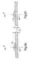
- integrated circuit package 10 of the present invention including leadframes 12, 14 in electrical communication with an integrated circuit 16.
- integrated circuit 16 includes an integrated circuit die 18 formed of a semiconductor material. Die 18 is sandwiched between non-conductive substrates 20, 22, which can be formed of a ceramic material.
- Each of substrates 20, 22 can include a respective layer of solderable material 24, 26 on the outer surfaces thereof. Pressure attached applications may not require solderable material 24, 26 on the outer surface. Elimination of solderable material 24 and 26 reduces the thermal resistance and device temperature.
- Electrode 28 is attached to an inner surface 32 of substrate 20.
- element 28 is in the form of a substrate, while element 30 may better be described as an electrical contact pad.
- Each of elements 28, 30 are electrically connected to other circuit elements within package 10, although elements 28, 30 can be electrically isolated from each other.
- Element 28 is in electrical communication with each of a distal end 34 of leadframe 12 and die 18.
- Element 30 is in electrical communication with a distal end 36 of leadframe 14.
- FIG. 1B there may be a layer 38 of electrically conductive attachment material disposed between element 28 and distal end 34 of leadframe 12. There may also be a layer 40 of electrically conductive attachment material disposed between element 30 and distal end 36 of leadframe 14, as shown in FIG. 1A .
- Electrode 42, 44 are attached to an inner surface 46 of substrate 22.
- element 44 is in the form of a substrate, while element 42 may better be described as an electrical contact pad.
- Each of elements 42, 44 are electrically connected to other circuit elements within package 10, although elements 42, 44 can be electrically isolated from each other.
- Element 44 is in electrical communication with each of a distal end 36 of leadframe 14 and die 18.
- Element 42 is in electrical communication with a distal end 34 of leadframe 12.
- a layer 48 of electrically conductive attachment material disposed between element 42 and distal end 34 of leadframe 12.
- a layer 50 of electrically conductive attachment material disposed between element 44 and distal end 36 of leadframe 14.
- the die attachment material of layers 38, 40, 48, 50 may be a type of solder paste, solder preform, ultra-thick thick film (UTTF), or electrically conductive adhesive, for example.
- die 18 has a thickness 52 as measured in a vertical direction.
- the thickness of die 18 limits how close together elements 28, 42 can be placed. More particularly, a distance between layers of attachment material 38, 48 is no less than thickness 52.
- a thickness 54 of a base portion 56 of a leadframe member 58 is not sufficiently large to perform any necessary bridging of the gap between layers of attachment material 38, 48. That is, it may be necessary for leadframe 12 to be in electrical communication with each of elements 28, 42.
- distal end 34 of leadframe member 58 is provided with an undulation 60 that, together with base portion 56, provides distal end 34 with a thickness greater than that of base portion 56 alone.
- undulation 60 together with base portion 56 provides distal end 34 with a thickness approximately equal to or slightly greater than thickness 52 of die 18.
- distal end 34 can simultaneously contact conductive attachment layers 38, 48 as well as enable desired thicknesses of layers 38, 48 to be maintained.
- An undulation such as undulation 60 may be provided below base portion 56, as is the case with leadframe 12.
- an undulation may be provided above base portion 56, as is the case with leadframe 14 as shown in FIG. 1A .
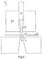
- Machine 62 that can be used in forming undulations such as undulation 60 is shown in FIG. 2 .
- Machine 62 includes a piston 64 that can drive a punch 66 in direction 68 to extrude or otherwise create an undulation 70 in an otherwise planar sheet 72 of copper stock from which a leadframe can be formed.
- the surface area of a "crest" 74 of undulation 70 as well as the effective thickness between crest 74 and an opposite base portion surface 76 can be controlled by the size and type of punch 66 and by the level of force with which punch 66 is driven.
- a solid die section (not shown) could be used to further control the size, shape, and thickness of undulation 70.
- Progressive die machine 62 or a similar progressive die machine, can be used to form or punch out the entire leadframe from a sheet of copper stock.
- FIGS. 3-8 Various embodiments of a leadframe of the present invention including a member having an undulated distal end will now be described with reference to FIGS. 3-8 .
- Each of the leadframe embodiments is suitable for use in conjunction with integrated circuit 16. It should be understood that although all of the leadframes of FIGS. 3-8 are shown with upwardly extending undulations, they can be easily modified within the scope of the invention to extend in a downward direction, i.e., in a direction away from the leadframe body.
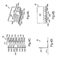
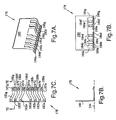
- FIGS. 3A-D illustrate one embodiment of a leadframe 78 of the present invention including a body 80 and a plurality of members 82a-g having proximal ends 84a-g and distal ends or "leads" 86a-g.
- leads 86a-g is offset formed such that the leads ramp up from the level of base portions 88a-g to a slightly higher vertical level, thereby providing leads 86a-g with undulations 90a-g.
- Undulations 90a-g and base portions 88a-g provide distal ends 86a-g with effective thicknesses greater than the thicknesses of base portions 88a-g alone.
- Each of leads 86a-g has a width in direction 92 that is greater than the width of the respective one of proximal ends 84a-g. Thus, there is ample width for leads 86a-g to ramp up to a desired vertical level without too steep of a slope.
- each of members 82a-g is bent at an angle of 90° such that distal ends 86a-g of members 82a-g extend in a direction perpendicular to body 80.
- members 82a-g define an imaginary plane 94.
- each of members 82a-g follows a bending path, i.e., is nonlinear, in a direction within plane 94.
- FIGS. 4A-D illustrate another embodiment of a leadframe 98 of the present invention including a body 100 and a plurality of members 102a-g having proximal ends 104a-g and distal ends or "leads" 106a-g.
- leads 106a-g is offset formed such that the leads ramp up from the level of base portions 108a-g to a slightly higher vertical level, thereby providing leads 106a-g with undulations 110a-g.
- Undulations 110a-g and base portions 108a-g provide distal ends 106a-g with effective thicknesses greater than the thicknesses of base portions 108a-g alone.
- Each of leads 106a-g ramps up in a direction 112 that is parallel to a direction in which members 102a-g generally extend.
- the machining of slits 113a-g and the punching of undulations 110a-g is facilitated, i.e., made easier.
- each of members 102a-g is bent at an angle of 90° such that distal ends 106a-g of members 102a-g extend in a direction perpendicular to body 100.
- members 102a-g define an imaginary plane 114.
- each of members 102a-g follows a bending path, i.e., is nonlinear, in a direction within plane 114.
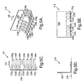
- FIGS. 5A-D illustrate yet another embodiment of a leadframe 118 of the present invention including a body 120 and a plurality of members 122a-g having proximal ends 124a-g and distal ends or "leads" 126a-g.
- leads 126a-g is corrugated formed such that the leads ramp up from the level of base portions 128a-g to a slightly higher vertical level, and then ramp back down to the level of base portions 128a-g, thereby providing leads 126a-g with undulations 130a-g.
- Undulations 130a-g and base portions 128a-g provide distal ends 126a-g with effective thicknesses greater than the thicknesses of base portions 128a-g alone.
- Each of leads 126a-g ramps up and down in a direction 132 that is parallel to a direction in which members 122a-g generally extend. Thus, the punching of undulations 130a-g is facilitated, i.e., made easier.
- each of members 122a-g is bent at an angle of 90° such that distal ends 126a-g of members 122a-g extend in a direction perpendicular to body 120.
- members 122a-g define an imaginary plane 134.
- each of members 122a-g follows a bending path, i.e., is nonlinear, in a direction within plane 134.
- Distal ends of leadframe members may have a single undulation, as is the case with the single undulation 130 on each of members 122a-g in FIGS. 5A-D .
- distal ends of leadframe member may have multiple undulations, as is the case with each of corrugated formed distal ends 136, 138 and 140.
- the undulations may be in the form of a sinusoidal wave, as with distal end 136; a triangle wave, as with distal end 138; or a substantially square wave, as with distal end 140, for example.
- a characteristic of corrugated undulations is that the undulation can extend completely across the width of the distal end in direction 142.
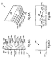
- FIGS. 6A-D illustrate a further embodiment of a leadframe 148 of the present invention including a body 150 and a plurality of members 152a-g having proximal ends 154a-g and distal ends or "leads" 156a-g.
- leads 156a-g is squirt formed such that the leads have dome-like bumps, thereby providing leads 156a-g with undulations 160a-g.
- Undulations 160a-g and base portions 158a-g provide distal ends 156a-g with effective thicknesses greater than the thicknesses of base portions 158a-g alone.
- each of members 152a-g is bent at an angle of 90° such that distal ends 156a-g of members 152a-g extend in a direction perpendicular to body 150.
- members 152a-g define an imaginary plane 164.
- each of members 152a-g follows a bending path, i.e., is nonlinear, in a direction within plane 164.
- the punch of the progressive die may form a squirt formed undulation having a concave, rounded cavity 166 or a trapezoidal cavity 168.
- a characteristic of squirt formed leads is that the depth of the cavity may be less than the thickness of the base portion.
- the depths of cavities 166, 168 in direction 170 is less than a thickness 172 of respective base portions 174, 176.
- FIGS. 7A-D illustrate still another embodiment of a leadframe 178 of the present invention including a body 180 and a plurality of members 182a-g having proximal ends 184a-g and distal ends or "leads" 186a-g.
- leads 186a-g is embossed formed such that the leads have bumps that are dome-like with the exception that they can have flat tops 187a-g, thereby providing leads 186a-g with undulations 190a-g.
- Undulations 190a-g and base portions 188a-g provide distal ends 186a-g with effective thicknesses greater than the thicknesses of base portions 188a-g alone.
- each of members 182a-g is bent at an angle of 90° such that distal ends 186a-g of members 182a-g extend in a direction perpendicular to body 180.
- members 182a-g define an imaginary plane 194.
- each of members 182a-g follows a bending path, i.e., is nonlinear, in a direction within plane 194.
- an embossed formed undulation can have an effective height 196 that is greater than twice a thickness 198 of a base portion 200.
- a characteristic of embossed formed leads is that the depth of the cavity may be greater than the thickness of the base portion. For example, the depths of cavity 202 in direction 204 is greater than a thickness 198 of base portion 200.
- FIGS. 8A-D illustrate still another embodiment of a leadframe 208 of the present invention including a body 210 and a plurality of members 212a-g having proximal ends 214a-g and distal ends or "leads" 216a-g.
- leads 216a-g is embossed formed such that the leads have oblong bumps that can have flat tops 217a-g and open ends 219a-g, thereby providing leads 216a-g with undulations 220a-g.
- Undulations 220a-g and base portions 218a-g provide distal ends 216a-g with effective thicknesses greater than the thicknesses of base portions 218a-g alone.
- each of members 212a-g is bent at an angle of 90° such that distal ends 216a-g of members 212a-g extend in a direction perpendicular to body 210.
- members 212a-g define an imaginary plane 224.
- each of members 212a-g follows a bending path, i.e., is nonlinear, in a direction within plane 224.
- an embossed formed, open-ended undulation can have an effective height 226 that is greater than twice a thickness 228 of a base portion 230.
- a characteristic of embossed formed leads is that the depth of the cavity may be greater than the thickness of the base portion. For example, the depths of cavity 232 in direction 234 is greater than a thickness 228 of base portion 230.
- a body portion is formed with a plurality of members extending from the body, with each of the members having a proximal end and a distal end.
- a progressive die machine such as machine 62 ( FIG. 2 ) can form a body 80 ( FIG. 3A ), for example, with members 82a-g extending from body 80.
- a punch (not shown) that is designed for the particular application can be used in machine 62 to form body 80 and members 82a-g from a sheet of copper stock.
- Members 82a-g have proximal ends 84a-g and distal ends 86a-g.
- a second step S904 an undulation is formed in each of the distal ends.
- undulations 90a-g can be formed in distal ends 86a-g by inserting in machine 62 a punch (not shown) that is designed to form undulations 90a-g.
- the leadframe members can be bent at an angle of approximately 90° such that the distal ends of the members extend in a direction substantially perpendicular to the body of the leadframe.
Landscapes
- Lead Frames For Integrated Circuits (AREA)
Claims (6)
- Verpackung (10) für integrierte Schaltung, die ein erstes nicht-leitendes Substrat (20) aufweist mit einer ersten inneren Oberfläche (32); einen Die (18) mit einer ersten Dicke (52); und einen Leiterrahmen (12), der ein Element (58) umfasst, das ein proximales Ende und ein distales Ende hat, wobei das proximale Ende eine zweite Dicke (54) hat, die geringer ist als die erste Dicke; gekennzeichnet durch ein zweites nicht-leitendes Substrat (22) mit einer zweiten inneren Oberfläche (46); wobei der Die (18) zwischen den ersten und zweiten inneren Oberflächen (32, 46) angeordnet ist; und wobei das distale Ende des Leiterrahmens (12) zwischen den ersten und zweiten inneren Oberflächen (32, 46) angeordnet ist, wobei das distale Ende wellenförmig (60) ist derart, dass das distale Ende eine effektive Dicke hat, die größer als die zweite Dicke ist.
- Verpackung gemäß Anspruch 1, dadurch gekennzeichnet, dass die effektive Dicke gleich zu der ersten Dicke ist.
- Verpackung gemäß Anspruch 1, dadurch gekennzeichnet, dass das distale Ende eines ist aus mit Versatz geformt, gewölbt-geformt, gewellt-geformt und erhaben-geformt.
- Verpackung gemäß Anspruch 1, gekennzeichnet durch zumindest ein erstes leitendes Element (28, 30), das an der ersten inneren Oberfläche befestigt ist und in elektrischer Verbindung mit sowohl dem distalen Ende des Elements als auch dem Die ist; und zumindest ein zweites leitendes Element (42, 44), das an der zweiten inneren Oberfläche befestigt ist und in elektrischer Verbindung mit sowohl dem distalen Ende des Elements als auch dem Die ist.
- Verpackung gemäß Anspruch 4, dadurch gekennzeichnet, dass das zumindest eine erste leitende Element zumindest ein erstes verbundenes Kupferelement aufweist, und das zumindest eine zweite leitende Element zumindest ein zweites verbundenes Kupferelement aufweist.
- Verpackung gemäß Anspruch 4, gekennzeichnet durch zumindest eine erste Schicht von leitendem Befestigungsmaterial (38, 40), die zwischen dem zumindest einen ersten leitenden Element und sowohl dem distalen Ende des Elements als auch dem Die angeordnet ist; und zumindest eine zweite Schicht von leitendem Befestigungsmaterial (48, 50), die zwischen dem zumindest einen zweiten leitenden Element und sowohl dem distalen Ende des Elements als auch dem Die angeordnet ist.
Applications Claiming Priority (2)
| Application Number | Priority Date | Filing Date | Title |
|---|---|---|---|
| US10/780,163 US7148564B2 (en) | 2004-02-17 | 2004-02-17 | Dual-sided substrate integrated circuit package including a leadframe having leads with increased thickness |
| US780163 | 2004-02-17 |
Publications (3)
| Publication Number | Publication Date |
|---|---|
| EP1564811A2 EP1564811A2 (de) | 2005-08-17 |
| EP1564811A3 EP1564811A3 (de) | 2007-08-08 |
| EP1564811B1 true EP1564811B1 (de) | 2012-01-11 |
Family
ID=34701440
Family Applications (1)
| Application Number | Title | Priority Date | Filing Date |
|---|---|---|---|
| EP05075241A Expired - Lifetime EP1564811B1 (de) | 2004-02-17 | 2005-01-31 | Verpackung für eine integrierte Schaltung mit je einem Substrat auf beiden Seiten und mit einem Leiterrahmen der Leiter mit erhöhter Dicke aufweist |
Country Status (3)
| Country | Link |
|---|---|
| US (4) | US7148564B2 (de) |
| EP (1) | EP1564811B1 (de) |
| AT (1) | ATE541313T1 (de) |
Families Citing this family (6)
| Publication number | Priority date | Publication date | Assignee | Title |
|---|---|---|---|---|
| US7148564B2 (en) * | 2004-02-17 | 2006-12-12 | Delphi Technologies, Inc. | Dual-sided substrate integrated circuit package including a leadframe having leads with increased thickness |
| JP2006222406A (ja) * | 2004-08-06 | 2006-08-24 | Denso Corp | 半導体装置 |
| US20080054496A1 (en) | 2006-08-30 | 2008-03-06 | Neill Thornton | High temperature operating package and circuit design |
| US20090001546A1 (en) * | 2007-06-28 | 2009-01-01 | Flederbach Lynda G | Ultra-thick thick film on ceramic substrate |
| CA2978795A1 (en) | 2015-03-16 | 2016-09-22 | Dana Canada Corporation | Heat exchangers with plates having surface patterns for enhancing flatness and methods for manufacturing same |
| KR102733494B1 (ko) | 2020-02-13 | 2024-11-25 | 엘지마그나 이파워트레인 주식회사 | 전력 모듈 |
Family Cites Families (21)
| Publication number | Priority date | Publication date | Assignee | Title |
|---|---|---|---|---|
| US3945808A (en) * | 1974-04-15 | 1976-03-23 | Amp Incorporated | Lead frame adapted for electrical switch package |
| JPS62254457A (ja) * | 1986-04-28 | 1987-11-06 | Nec Corp | Ic用リ−ドフレ−ム |
| US5166098A (en) * | 1988-03-05 | 1992-11-24 | Deutsche Itt Industries Gmbh | Method of manufacturing an encapsulated semiconductor device with a can type housing |
| JPH0547980A (ja) * | 1991-08-08 | 1993-02-26 | Sumitomo Metal Mining Co Ltd | 半導体装置用icリ−ドフレ−ム |
| JPH06252334A (ja) * | 1993-02-26 | 1994-09-09 | Hitachi Constr Mach Co Ltd | 半導体装置 |
| US5340771A (en) * | 1993-03-18 | 1994-08-23 | Lsi Logic Corporation | Techniques for providing high I/O count connections to semiconductor dies |
| KR100386061B1 (ko) * | 1995-10-24 | 2003-08-21 | 오끼 덴끼 고오교 가부시끼가이샤 | 크랙을방지하기위한개량된구조를가지는반도체장치및리이드프레임 |
| KR100186309B1 (ko) * | 1996-05-17 | 1999-03-20 | 문정환 | 적층형 버텀 리드 패키지 |
| US5677567A (en) * | 1996-06-17 | 1997-10-14 | Micron Technology, Inc. | Leads between chips assembly |
| US6072228A (en) * | 1996-10-25 | 2000-06-06 | Micron Technology, Inc. | Multi-part lead frame with dissimilar materials and method of manufacturing |
| JP3487173B2 (ja) * | 1997-05-26 | 2004-01-13 | セイコーエプソン株式会社 | Tab用テープキャリア、集積回路装置及び電子機器 |
| JPH11288751A (ja) * | 1998-04-03 | 1999-10-19 | Alps Electric Co Ltd | プリント配線基板への端子の取付構造 |
| US6122822A (en) * | 1998-06-23 | 2000-09-26 | Vanguard International Semiconductor Corporation | Method for balancing mold flow in encapsulating devices |
| US6307755B1 (en) * | 1999-05-27 | 2001-10-23 | Richard K. Williams | Surface mount semiconductor package, die-leadframe combination and leadframe therefor and method of mounting leadframes to surfaces of semiconductor die |
| JP4416140B2 (ja) * | 2000-04-14 | 2010-02-17 | 日本インター株式会社 | 樹脂封止型半導体装置 |
| US6781225B2 (en) * | 2000-09-15 | 2004-08-24 | Chipmos Technologies Inc. | Glueless integrated circuit system in a packaging module |
| US6459148B1 (en) * | 2000-11-13 | 2002-10-01 | Walsin Advanced Electronics Ltd | QFN semiconductor package |
| US6812553B2 (en) * | 2002-01-16 | 2004-11-02 | Delphi Technologies, Inc. | Electrically isolated and thermally conductive double-sided pre-packaged component |
| TW540123B (en) * | 2002-06-14 | 2003-07-01 | Siliconware Precision Industries Co Ltd | Flip-chip semiconductor package with lead frame as chip carrier |
| US7148564B2 (en) * | 2004-02-17 | 2006-12-12 | Delphi Technologies, Inc. | Dual-sided substrate integrated circuit package including a leadframe having leads with increased thickness |
| US7202105B2 (en) * | 2004-06-28 | 2007-04-10 | Semiconductor Components Industries, L.L.C. | Multi-chip semiconductor connector assembly method |
-
2004
- 2004-02-17 US US10/780,163 patent/US7148564B2/en not_active Expired - Lifetime
-
2005
- 2005-01-31 AT AT05075241T patent/ATE541313T1/de active
- 2005-01-31 EP EP05075241A patent/EP1564811B1/de not_active Expired - Lifetime
-
2006
- 2006-10-05 US US11/543,605 patent/US20070069348A1/en not_active Abandoned
-
2008
- 2008-04-24 US US12/150,070 patent/US7697303B2/en not_active Expired - Lifetime
-
2010
- 2010-02-02 US US12/698,644 patent/US20100133672A1/en not_active Abandoned
Also Published As
| Publication number | Publication date |
|---|---|
| US20100133672A1 (en) | 2010-06-03 |
| US20050179123A1 (en) | 2005-08-18 |
| US20080198568A1 (en) | 2008-08-21 |
| US7697303B2 (en) | 2010-04-13 |
| EP1564811A3 (de) | 2007-08-08 |
| US20070069348A1 (en) | 2007-03-29 |
| ATE541313T1 (de) | 2012-01-15 |
| EP1564811A2 (de) | 2005-08-17 |
| US7148564B2 (en) | 2006-12-12 |
Similar Documents
| Publication | Publication Date | Title |
|---|---|---|
| US7025601B2 (en) | Interposer and method for making same | |
| KR100206049B1 (ko) | 가소 성형 집적 회로 패키지 | |
| JP2934202B2 (ja) | 配線基板における導電バンプの形成方法 | |
| US6208521B1 (en) | Film carrier and laminate type mounting structure using same | |
| US7697303B2 (en) | Dual-sided substrate integrated circuit package including a leadframe having leads with increased thickness | |
| CN1110772C (zh) | 芯片模块 | |
| TWI311836B (en) | Electrical connecting member capable of achieving stable connection with a simple structure and connector using the same | |
| EP1304740A3 (de) | Leiterplatte, ihre Herstellungsmethode und Modul hoher Ausgangsleistung | |
| TW200425445A (en) | Lead frame, method of manufacturing the same, semiconductor device using lead frame and method of manufacturing semiconductor device | |
| KR20050011714A (ko) | 휨저항성 기부판을 갖는 전력 반도체 모듈 | |
| KR100457029B1 (ko) | 랜드 그리드 어레이형 반도체장치 및 그의 실장방법 | |
| US20050225957A1 (en) | Connnecting device for contacting a semiconductor component | |
| US6633077B2 (en) | Semiconductor device and method for manufacturing the same | |
| WO2002093649A3 (fr) | Module electronique et son procede d'assemblage | |
| EP1610381A3 (de) | Elektonikgehäuse mit segmentierten Verbindungen und Lotverbindung | |
| US5514839A (en) | Weldable flexible circuit termination for high temperature applications | |
| JP2005285909A (ja) | 混成集積回路装置の製造方法 | |
| KR20020034923A (ko) | 금속 지지 프레임의 제조 방법, 상기 금속 지지 프레임 및이의 이용 | |
| US7560809B2 (en) | Semiconductor device | |
| CN1458688A (zh) | 电子组件 | |
| US20080290481A1 (en) | Semiconductor Device Package Leadframe | |
| JPH09214093A (ja) | 実装回路装置およびその製造方法 | |
| US12068236B2 (en) | Electronic module | |
| JPH08330501A (ja) | 半導体のリードフレームおよびその製造方法 | |
| JP2954559B2 (ja) | 配線基板の電極構造 |
Legal Events
| Date | Code | Title | Description |
|---|---|---|---|
| PUAI | Public reference made under article 153(3) epc to a published international application that has entered the european phase |
Free format text: ORIGINAL CODE: 0009012 |
|
| AK | Designated contracting states |
Kind code of ref document: A2 Designated state(s): AT BE BG CH CY CZ DE DK EE ES FI FR GB GR HU IE IS IT LI LT LU MC NL PL PT RO SE SI SK TR |
|
| AX | Request for extension of the european patent |
Extension state: AL BA HR LV MK YU |
|
| PUAL | Search report despatched |
Free format text: ORIGINAL CODE: 0009013 |
|
| AK | Designated contracting states |
Kind code of ref document: A3 Designated state(s): AT BE BG CH CY CZ DE DK EE ES FI FR GB GR HU IE IS IT LI LT LU MC NL PL PT RO SE SI SK TR |
|
| AX | Request for extension of the european patent |
Extension state: AL BA HR LV MK YU |
|
| 17P | Request for examination filed |
Effective date: 20080208 |
|
| AKX | Designation fees paid |
Designated state(s): AT BE BG CH CY CZ DE DK EE ES FI FR GB GR HU IE IS IT LI LT LU MC NL PL PT RO SE SI SK TR |
|
| 17Q | First examination report despatched |
Effective date: 20091106 |
|
| GRAP | Despatch of communication of intention to grant a patent |
Free format text: ORIGINAL CODE: EPIDOSNIGR1 |
|
| GRAS | Grant fee paid |
Free format text: ORIGINAL CODE: EPIDOSNIGR3 |
|
| GRAA | (expected) grant |
Free format text: ORIGINAL CODE: 0009210 |
|
| AK | Designated contracting states |
Kind code of ref document: B1 Designated state(s): AT BE BG CH CY CZ DE DK EE ES FI FR GB GR HU IE IS IT LI LT LU MC NL PL PT RO SE SI SK TR |
|
| REG | Reference to a national code |
Ref country code: GB Ref legal event code: FG4D |
|
| REG | Reference to a national code |
Ref country code: CH Ref legal event code: EP |
|
| REG | Reference to a national code |
Ref country code: AT Ref legal event code: REF Ref document number: 541313 Country of ref document: AT Kind code of ref document: T Effective date: 20120115 |
|
| REG | Reference to a national code |
Ref country code: IE Ref legal event code: FG4D |
|
| REG | Reference to a national code |
Ref country code: DE Ref legal event code: R096 Ref document number: 602005032066 Country of ref document: DE Effective date: 20120308 |
|
| REG | Reference to a national code |
Ref country code: NL Ref legal event code: VDEP Effective date: 20120111 |
|
| PG25 | Lapsed in a contracting state [announced via postgrant information from national office to epo] |
Ref country code: SI Free format text: LAPSE BECAUSE OF FAILURE TO SUBMIT A TRANSLATION OF THE DESCRIPTION OR TO PAY THE FEE WITHIN THE PRESCRIBED TIME-LIMIT Effective date: 20120111 |
|
| LTIE | Lt: invalidation of european patent or patent extension |
Effective date: 20120111 |
|
| PG25 | Lapsed in a contracting state [announced via postgrant information from national office to epo] |
Ref country code: NL Free format text: LAPSE BECAUSE OF FAILURE TO SUBMIT A TRANSLATION OF THE DESCRIPTION OR TO PAY THE FEE WITHIN THE PRESCRIBED TIME-LIMIT Effective date: 20120111 Ref country code: BE Free format text: LAPSE BECAUSE OF FAILURE TO SUBMIT A TRANSLATION OF THE DESCRIPTION OR TO PAY THE FEE WITHIN THE PRESCRIBED TIME-LIMIT Effective date: 20120111 Ref country code: LT Free format text: LAPSE BECAUSE OF FAILURE TO SUBMIT A TRANSLATION OF THE DESCRIPTION OR TO PAY THE FEE WITHIN THE PRESCRIBED TIME-LIMIT Effective date: 20120111 Ref country code: BG Free format text: LAPSE BECAUSE OF FAILURE TO SUBMIT A TRANSLATION OF THE DESCRIPTION OR TO PAY THE FEE WITHIN THE PRESCRIBED TIME-LIMIT Effective date: 20120411 Ref country code: IS Free format text: LAPSE BECAUSE OF FAILURE TO SUBMIT A TRANSLATION OF THE DESCRIPTION OR TO PAY THE FEE WITHIN THE PRESCRIBED TIME-LIMIT Effective date: 20120511 |
|
| PG25 | Lapsed in a contracting state [announced via postgrant information from national office to epo] |
Ref country code: GR Free format text: LAPSE BECAUSE OF FAILURE TO SUBMIT A TRANSLATION OF THE DESCRIPTION OR TO PAY THE FEE WITHIN THE PRESCRIBED TIME-LIMIT Effective date: 20120412 Ref country code: MC Free format text: LAPSE BECAUSE OF NON-PAYMENT OF DUE FEES Effective date: 20120131 Ref country code: FI Free format text: LAPSE BECAUSE OF FAILURE TO SUBMIT A TRANSLATION OF THE DESCRIPTION OR TO PAY THE FEE WITHIN THE PRESCRIBED TIME-LIMIT Effective date: 20120111 Ref country code: PT Free format text: LAPSE BECAUSE OF FAILURE TO SUBMIT A TRANSLATION OF THE DESCRIPTION OR TO PAY THE FEE WITHIN THE PRESCRIBED TIME-LIMIT Effective date: 20120511 Ref country code: PL Free format text: LAPSE BECAUSE OF FAILURE TO SUBMIT A TRANSLATION OF THE DESCRIPTION OR TO PAY THE FEE WITHIN THE PRESCRIBED TIME-LIMIT Effective date: 20120111 |
|
| REG | Reference to a national code |
Ref country code: CH Ref legal event code: PL |
|
| REG | Reference to a national code |
Ref country code: AT Ref legal event code: MK05 Ref document number: 541313 Country of ref document: AT Kind code of ref document: T Effective date: 20120111 |
|
| PG25 | Lapsed in a contracting state [announced via postgrant information from national office to epo] |
Ref country code: CY Free format text: LAPSE BECAUSE OF FAILURE TO SUBMIT A TRANSLATION OF THE DESCRIPTION OR TO PAY THE FEE WITHIN THE PRESCRIBED TIME-LIMIT Effective date: 20120111 |
|
| REG | Reference to a national code |
Ref country code: IE Ref legal event code: MM4A |
|
| PG25 | Lapsed in a contracting state [announced via postgrant information from national office to epo] |
Ref country code: LI Free format text: LAPSE BECAUSE OF NON-PAYMENT OF DUE FEES Effective date: 20120131 Ref country code: RO Free format text: LAPSE BECAUSE OF FAILURE TO SUBMIT A TRANSLATION OF THE DESCRIPTION OR TO PAY THE FEE WITHIN THE PRESCRIBED TIME-LIMIT Effective date: 20120111 Ref country code: SE Free format text: LAPSE BECAUSE OF FAILURE TO SUBMIT A TRANSLATION OF THE DESCRIPTION OR TO PAY THE FEE WITHIN THE PRESCRIBED TIME-LIMIT Effective date: 20120111 Ref country code: DK Free format text: LAPSE BECAUSE OF FAILURE TO SUBMIT A TRANSLATION OF THE DESCRIPTION OR TO PAY THE FEE WITHIN THE PRESCRIBED TIME-LIMIT Effective date: 20120111 Ref country code: CZ Free format text: LAPSE BECAUSE OF FAILURE TO SUBMIT A TRANSLATION OF THE DESCRIPTION OR TO PAY THE FEE WITHIN THE PRESCRIBED TIME-LIMIT Effective date: 20120111 Ref country code: EE Free format text: LAPSE BECAUSE OF FAILURE TO SUBMIT A TRANSLATION OF THE DESCRIPTION OR TO PAY THE FEE WITHIN THE PRESCRIBED TIME-LIMIT Effective date: 20120111 Ref country code: CH Free format text: LAPSE BECAUSE OF NON-PAYMENT OF DUE FEES Effective date: 20120131 |
|
| PLBE | No opposition filed within time limit |
Free format text: ORIGINAL CODE: 0009261 |
|
| STAA | Information on the status of an ep patent application or granted ep patent |
Free format text: STATUS: NO OPPOSITION FILED WITHIN TIME LIMIT |
|
| PG25 | Lapsed in a contracting state [announced via postgrant information from national office to epo] |
Ref country code: IT Free format text: LAPSE BECAUSE OF FAILURE TO SUBMIT A TRANSLATION OF THE DESCRIPTION OR TO PAY THE FEE WITHIN THE PRESCRIBED TIME-LIMIT Effective date: 20120111 Ref country code: SK Free format text: LAPSE BECAUSE OF FAILURE TO SUBMIT A TRANSLATION OF THE DESCRIPTION OR TO PAY THE FEE WITHIN THE PRESCRIBED TIME-LIMIT Effective date: 20120111 |
|
| 26N | No opposition filed |
Effective date: 20121012 |
|
| GBPC | Gb: european patent ceased through non-payment of renewal fee |
Effective date: 20120411 |
|
| PG25 | Lapsed in a contracting state [announced via postgrant information from national office to epo] |
Ref country code: IE Free format text: LAPSE BECAUSE OF NON-PAYMENT OF DUE FEES Effective date: 20120131 Ref country code: AT Free format text: LAPSE BECAUSE OF FAILURE TO SUBMIT A TRANSLATION OF THE DESCRIPTION OR TO PAY THE FEE WITHIN THE PRESCRIBED TIME-LIMIT Effective date: 20120111 Ref country code: GB Free format text: LAPSE BECAUSE OF NON-PAYMENT OF DUE FEES Effective date: 20120411 |
|
| REG | Reference to a national code |
Ref country code: DE Ref legal event code: R097 Ref document number: 602005032066 Country of ref document: DE Effective date: 20121012 |
|
| REG | Reference to a national code |
Ref country code: FR Ref legal event code: ST Effective date: 20130104 |
|
| PG25 | Lapsed in a contracting state [announced via postgrant information from national office to epo] |
Ref country code: FR Free format text: LAPSE BECAUSE OF NON-PAYMENT OF DUE FEES Effective date: 20120312 |
|
| PG25 | Lapsed in a contracting state [announced via postgrant information from national office to epo] |
Ref country code: ES Free format text: LAPSE BECAUSE OF FAILURE TO SUBMIT A TRANSLATION OF THE DESCRIPTION OR TO PAY THE FEE WITHIN THE PRESCRIBED TIME-LIMIT Effective date: 20120422 |
|
| PG25 | Lapsed in a contracting state [announced via postgrant information from national office to epo] |
Ref country code: TR Free format text: LAPSE BECAUSE OF FAILURE TO SUBMIT A TRANSLATION OF THE DESCRIPTION OR TO PAY THE FEE WITHIN THE PRESCRIBED TIME-LIMIT Effective date: 20120111 |
|
| PG25 | Lapsed in a contracting state [announced via postgrant information from national office to epo] |
Ref country code: LU Free format text: LAPSE BECAUSE OF NON-PAYMENT OF DUE FEES Effective date: 20120131 |
|
| PG25 | Lapsed in a contracting state [announced via postgrant information from national office to epo] |
Ref country code: HU Free format text: LAPSE BECAUSE OF FAILURE TO SUBMIT A TRANSLATION OF THE DESCRIPTION OR TO PAY THE FEE WITHIN THE PRESCRIBED TIME-LIMIT Effective date: 20050131 |
|
| REG | Reference to a national code |
Ref country code: DE Ref legal event code: R081 Ref document number: 602005032066 Country of ref document: DE Owner name: DELPHI TECHNOLOGIES IP LIMITED, BB Free format text: FORMER OWNER: DELPHI TECHNOLOGIES, INC., TROY, MICH., US |
|
| P01 | Opt-out of the competence of the unified patent court (upc) registered |
Effective date: 20230327 |
|
| PGFP | Annual fee paid to national office [announced via postgrant information from national office to epo] |
Ref country code: DE Payment date: 20231215 Year of fee payment: 20 |
|
| REG | Reference to a national code |
Ref country code: DE Ref legal event code: R071 Ref document number: 602005032066 Country of ref document: DE |