EP1562200A2 - Nichtflüchtige Halbleiterspeicheranordnung - Google Patents
Nichtflüchtige Halbleiterspeicheranordnung Download PDFInfo
- Publication number
- EP1562200A2 EP1562200A2 EP05250628A EP05250628A EP1562200A2 EP 1562200 A2 EP1562200 A2 EP 1562200A2 EP 05250628 A EP05250628 A EP 05250628A EP 05250628 A EP05250628 A EP 05250628A EP 1562200 A2 EP1562200 A2 EP 1562200A2
- Authority
- EP
- European Patent Office
- Prior art keywords
- memory cell
- readout
- voltage
- memory
- threshold voltage
- Prior art date
- Legal status (The legal status is an assumption and is not a legal conclusion. Google has not performed a legal analysis and makes no representation as to the accuracy of the status listed.)
- Withdrawn
Links
Images


Classifications
-
- B—PERFORMING OPERATIONS; TRANSPORTING
- B03—SEPARATION OF SOLID MATERIALS USING LIQUIDS OR USING PNEUMATIC TABLES OR JIGS; MAGNETIC OR ELECTROSTATIC SEPARATION OF SOLID MATERIALS FROM SOLID MATERIALS OR FLUIDS; SEPARATION BY HIGH-VOLTAGE ELECTRIC FIELDS
- B03D—FLOTATION; DIFFERENTIAL SEDIMENTATION
- B03D1/00—Flotation
- B03D1/14—Flotation machines
- B03D1/1431—Dissolved air flotation machines
-
- G—PHYSICS
- G11—INFORMATION STORAGE
- G11C—STATIC STORES
- G11C16/00—Erasable programmable read-only memories
- G11C16/02—Erasable programmable read-only memories electrically programmable
- G11C16/06—Auxiliary circuits, e.g. for writing into memory
- G11C16/26—Sensing or reading circuits; Data output circuits
- G11C16/28—Sensing or reading circuits; Data output circuits using differential sensing or reference cells, e.g. dummy cells
-
- B—PERFORMING OPERATIONS; TRANSPORTING
- B01—PHYSICAL OR CHEMICAL PROCESSES OR APPARATUS IN GENERAL
- B01D—SEPARATION
- B01D21/00—Separation of suspended solid particles from liquids by sedimentation
- B01D21/0027—Floating sedimentation devices
-
- B—PERFORMING OPERATIONS; TRANSPORTING
- B01—PHYSICAL OR CHEMICAL PROCESSES OR APPARATUS IN GENERAL
- B01F—MIXING, e.g. DISSOLVING, EMULSIFYING OR DISPERSING
- B01F23/00—Mixing according to the phases to be mixed, e.g. dispersing or emulsifying
- B01F23/20—Mixing gases with liquids
- B01F23/23—Mixing gases with liquids by introducing gases into liquid media, e.g. for producing aerated liquids
- B01F23/231—Mixing gases with liquids by introducing gases into liquid media, e.g. for producing aerated liquids by bubbling
-
- C—CHEMISTRY; METALLURGY
- C02—TREATMENT OF WATER, WASTE WATER, SEWAGE, OR SLUDGE
- C02F—TREATMENT OF WATER, WASTE WATER, SEWAGE, OR SLUDGE
- C02F1/00—Treatment of water, waste water, or sewage
- C02F1/24—Treatment of water, waste water, or sewage by flotation
-
- G—PHYSICS
- G11—INFORMATION STORAGE
- G11C—STATIC STORES
- G11C11/00—Digital stores characterised by the use of particular electric or magnetic storage elements; Storage elements therefor
- G11C11/56—Digital stores characterised by the use of particular electric or magnetic storage elements; Storage elements therefor using storage elements with more than two stable states represented by steps, e.g. of voltage, current, phase, frequency
- G11C11/5621—Digital stores characterised by the use of particular electric or magnetic storage elements; Storage elements therefor using storage elements with more than two stable states represented by steps, e.g. of voltage, current, phase, frequency using charge storage in a floating gate
- G11C11/5642—Sensing or reading circuits; Data output circuits
-
- G—PHYSICS
- G11—INFORMATION STORAGE
- G11C—STATIC STORES
- G11C11/00—Digital stores characterised by the use of particular electric or magnetic storage elements; Storage elements therefor
- G11C11/56—Digital stores characterised by the use of particular electric or magnetic storage elements; Storage elements therefor using storage elements with more than two stable states represented by steps, e.g. of voltage, current, phase, frequency
- G11C11/5678—Digital stores characterised by the use of particular electric or magnetic storage elements; Storage elements therefor using storage elements with more than two stable states represented by steps, e.g. of voltage, current, phase, frequency using amorphous/crystalline phase transition storage elements
-
- G—PHYSICS
- G11—INFORMATION STORAGE
- G11C—STATIC STORES
- G11C11/00—Digital stores characterised by the use of particular electric or magnetic storage elements; Storage elements therefor
- G11C11/56—Digital stores characterised by the use of particular electric or magnetic storage elements; Storage elements therefor using storage elements with more than two stable states represented by steps, e.g. of voltage, current, phase, frequency
- G11C11/5685—Digital stores characterised by the use of particular electric or magnetic storage elements; Storage elements therefor using storage elements with more than two stable states represented by steps, e.g. of voltage, current, phase, frequency using storage elements comprising metal oxide memory material, e.g. perovskites
-
- G—PHYSICS
- G11—INFORMATION STORAGE
- G11C—STATIC STORES
- G11C13/00—Digital stores characterised by the use of storage elements not covered by groups G11C11/00, G11C23/00, or G11C25/00
- G11C13/0002—Digital stores characterised by the use of storage elements not covered by groups G11C11/00, G11C23/00, or G11C25/00 using resistive RAM [RRAM] elements
- G11C13/0004—Digital stores characterised by the use of storage elements not covered by groups G11C11/00, G11C23/00, or G11C25/00 using resistive RAM [RRAM] elements comprising amorphous/crystalline phase transition cells
-
- G—PHYSICS
- G11—INFORMATION STORAGE
- G11C—STATIC STORES
- G11C13/00—Digital stores characterised by the use of storage elements not covered by groups G11C11/00, G11C23/00, or G11C25/00
- G11C13/0002—Digital stores characterised by the use of storage elements not covered by groups G11C11/00, G11C23/00, or G11C25/00 using resistive RAM [RRAM] elements
- G11C13/0007—Digital stores characterised by the use of storage elements not covered by groups G11C11/00, G11C23/00, or G11C25/00 using resistive RAM [RRAM] elements comprising metal oxide memory material, e.g. perovskites
-
- G—PHYSICS
- G11—INFORMATION STORAGE
- G11C—STATIC STORES
- G11C13/00—Digital stores characterised by the use of storage elements not covered by groups G11C11/00, G11C23/00, or G11C25/00
- G11C13/0002—Digital stores characterised by the use of storage elements not covered by groups G11C11/00, G11C23/00, or G11C25/00 using resistive RAM [RRAM] elements
- G11C13/0021—Auxiliary circuits
- G11C13/004—Reading or sensing circuits or methods
-
- G—PHYSICS
- G11—INFORMATION STORAGE
- G11C—STATIC STORES
- G11C13/00—Digital stores characterised by the use of storage elements not covered by groups G11C11/00, G11C23/00, or G11C25/00
- G11C13/0002—Digital stores characterised by the use of storage elements not covered by groups G11C11/00, G11C23/00, or G11C25/00 using resistive RAM [RRAM] elements
- G11C13/0021—Auxiliary circuits
- G11C13/0064—Verifying circuits or methods
-
- G—PHYSICS
- G11—INFORMATION STORAGE
- G11C—STATIC STORES
- G11C16/00—Erasable programmable read-only memories
- G11C16/02—Erasable programmable read-only memories electrically programmable
- G11C16/06—Auxiliary circuits, e.g. for writing into memory
- G11C16/34—Determination of programming status, e.g. threshold voltage, overprogramming or underprogramming, retention
- G11C16/3436—Arrangements for verifying correct programming or erasure
-
- C—CHEMISTRY; METALLURGY
- C02—TREATMENT OF WATER, WASTE WATER, SEWAGE, OR SLUDGE
- C02F—TREATMENT OF WATER, WASTE WATER, SEWAGE, OR SLUDGE
- C02F2209/00—Controlling or monitoring parameters in water treatment
- C02F2209/02—Temperature
-
- C—CHEMISTRY; METALLURGY
- C02—TREATMENT OF WATER, WASTE WATER, SEWAGE, OR SLUDGE
- C02F—TREATMENT OF WATER, WASTE WATER, SEWAGE, OR SLUDGE
- C02F2209/00—Controlling or monitoring parameters in water treatment
- C02F2209/42—Liquid level
-
- G—PHYSICS
- G11—INFORMATION STORAGE
- G11C—STATIC STORES
- G11C13/00—Digital stores characterised by the use of storage elements not covered by groups G11C11/00, G11C23/00, or G11C25/00
- G11C13/0002—Digital stores characterised by the use of storage elements not covered by groups G11C11/00, G11C23/00, or G11C25/00 using resistive RAM [RRAM] elements
- G11C13/0021—Auxiliary circuits
- G11C13/004—Reading or sensing circuits or methods
- G11C2013/0054—Read is performed on a reference element, e.g. cell, and the reference sensed value is used to compare the sensed value of the selected cell
-
- G—PHYSICS
- G11—INFORMATION STORAGE
- G11C—STATIC STORES
- G11C2213/00—Indexing scheme relating to G11C13/00 for features not covered by this group
- G11C2213/30—Resistive cell, memory material aspects
- G11C2213/31—Material having complex metal oxide, e.g. perovskite structure
Definitions
- the present invention relates to a nonvolatile semiconductor memory device such as a flash memory and more particularly, it relates to a constitution of a reference cell which is a reference at the time of readout, or at the time of verification for program or erase of a memory cell of the nonvolatile semiconductor memory device.
- each memory cell comprises a memory transistor having a floating gate structure and information is stored according to an amount of charges (electrons) input to the floating gate of each memory cell. More specifically, when many electrons are stored in the floating gate, an inversion layer is not likely to be formed in a channel region, so that the threshold voltage of the memory cell becomes high (which is defined as a programmed state).
- the inversion layer is likely to be formed in the channel region and the threshold voltage of the memory cell becomes low (which is defined as an erased state).
- a reference memory cell having a middle threshold voltage between the programmed state and the erased state is input to a differential input type of sense amplifier.
- the state in which the charge quantity is smallest is "11", which corresponds to the erased state.
- the charges are injected to the floating gate of the memory cell, which operation is called a program operation.
- the program operation can be performed only in the direction in which the charges of the floating gate are increased. For example, in order to transit from the state "01" to the state "10", it is necessary to perform the erase operation once to implement the state "11" and then to perform the program operation to implement the state "10".
- the program operation can be performed by a memory cell, the erase operation is performed by the plural memory cells.
- a program command is input through an I/O pad 22 and an address of the memory cell for the program operation is input through an address pad 1 to be specified in a first cycle.
- the inputted command is decoded by a command decoder 23 and when it is the program command, command decoder 23 directs a control circuit 13 to controls data (program data) inputted from the I/O pad 22 so as to be programmed in the address inputted from the address pad 1 in a second cycle.
- the address of the memory cell for the program operation is decoded in a main row decoder 4 and a main column decoder 8 through an address multiplexer 3 and at the same time, the plural number (eight, for example) of flash cells are selected.
- channel hot electrons which are generated when the source of the memory cell transistor is set at 0 V and a high voltage is applied to its gate and drain are injected into the floating gate.
- a pulse pattern generated in a program circuit 12 based on the program data determines whether the data is programmed in the selected memory cell or which storage state is implemented.
- the voltage which is divided from the high voltage, for example 12 V raised by a pumping circuit 14 depending on the storage state (threshold voltage) for the programming is outputted from a digital/analog converter circuit (D2A) 16 and is applied to the gate of the memory cell through the main row decoder 4.
- D2A digital/analog converter circuit
- a voltage, 5 V, for example is applied only to the drain of the memory cell for the program in the selected memory cell through the program circuit 12 and the main column decoder 8 for a certain period of time (program pulse).
- a voltage 0 V is applied to the drains of the cells which are not for the program so that the charges are not injected thereto to prevent the threshold voltage from being changed (that is, programmed).
- the program pulse After the program pulse is applied, it is verified whether the desired threshold voltage is attained by comparing it with the threshold voltage of the reference memory cell of a reference array 11 selected by a reference column decoder 7 and a reference row decoder 5, by the sense amplifier 9.
- the verifying operation is a kind of the readout operation, it is performed in order to secure the operation margin at the time of reading. Therefore, the operation margin is provided by setting the threshold voltage of the reference cell to be used at the time of the verification so as to be different from the threshold voltage of the reference cell to be used at the time of the reading when a wafer is tested.
- the verifying operation will be described with reference to Fig 1. Since the selection of the memory cell is the same as at the time of the programming, its description will be omitted.
- the verifying operation is performed by setting the source, the drain, and the gate of the memory cell at 0 V, at a low voltage (1 V, for example), at a readout voltage (6 V, for example), respectively.
- This voltage setting is in common with the memory cell of a main memory array 10 and the reference memory cell of the reference array 11, and the voltage which is raised by the pumping circuit 14 and divided by the D2A 16 is applied to the main memory array 10 through a main high-voltage switch circuit 17 and to the reference array 11 through a reference high-voltage switch circuit 18.
- a signal level "1" (showing that the programming is not completed yet), for example is sent from the sense amplifier 9 to the program circuit 12 and then the program pulse is applied again. After the pulse is applied, the verifying operation is performed again, so that the program pulse is applied until the sense amplifier 9 outputs the signal level "0" (showing that the programming is completed).
- the threshold voltage difference between the two memory cells to be input to the sense amplifier is larger, the data can be read more stably at higher speed. That is, as the threshold voltage difference (PV2 - M) is larger, the readout margin is increased.
- the threshold voltage for the ordinal readout is distinguished from the threshold voltage for the verifying operation in order to provide enough readout margin, and there are prepared the plural reference memory cells which are individually set by the program state so as to correspond to the multiple-level memory (refer to JP-A 59-104796 and JP-A 2002-100192, for example).
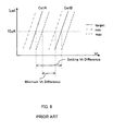
- the threshold voltage of each reference memory cell is set using a tester at the time of a test, when the threshold voltage setting of the reference memory cell (Cell A) for the readout and the reference memory cell (Cell B) for the verification are shifted by the error of the tester as shown in Fig. 8, it is considered that the provided threshold voltage difference could be smaller than the set threshold voltage difference. More specifically, when the threshold voltage of the reference memory cell for the verification is shifted in the negative direction and the threshold voltage of the reference memory cell for the readout is shifted in the positive direction, the threshold voltage difference becomes smaller than the set value. If such shifts occur, there is a problem such that the operation margin at the time of the readout becomes small.
- the memory cell tends to become a multi-level cell and it is necessary to provide the reference memory cells having the many kinds of threshold voltages in order to determine many storage levels. That is, the number of the reference memory cells and level sense circuits incidental to them are increased.
- the following problems are generated when the threshold voltage of the reference memory cell is set (referred to as "trimming") at the time of the test in the conventional nonvolatile semiconductor memory device. That is, since the number of the reference memory cells of the nonvolatile semiconductor memory device is increased because of an increase in capacity, multi-level memory and the like, the number of the reference memory cells to be trimmed is increased. In addition, although high precision of the trimming of the reference memory cell is required because of the multi-level cells, as the number of the reference cells is increased and as the trimming step becomes finer to provide higher precision, the trimming time is more increased; this causes production efficiency to be lowered.
- the present invention was made in view of the above problems and it is an object of the present invention to provide a semiconductor memory device in which the problems regarding the trimming of the reference memory cell are solved and multi-level cells can be handled and a readout operation can be performed stably at high speed.
- a nonvolatile semiconductor memory device to attain the above object is characterized by first characteristics in that it comprises a main memory array comprising a plurality of arranged memory cells having a nonvolatile memory element, at least one reference memory cell having the nonvolatile memory element, an address selection circuit which selects a particular memory cell from the main memory array, a readout circuit which reads data stored in the memory cell selected by the address selection circuit, by applying a predetermined electric stress to the selected memory cell and the reference memory cell so that currents corresponding to the respective storage states may flow, and comparing the current flowing in the selected memory cell with the current flowing in the reference memory cell, and a program circuit which programs data in the memory cell selected by the address selection circuit, and the readout circuit commonly uses the reference memory cell set in the same storage state at the time of normal readout and at the time of readout for program verification, and sets an applying condition to the reference memory cell such that its storage state may be shifted more in the program state direction than that in an applying condition at the time of the normal readout when
- the nonvolatile memory element is a nonvolatile memory transistor having an FET structure in which a threshold voltage is changed depending on a storage state
- the readout circuit applies a voltage at the same level to a gate of the nonvolatile memory transistor of each of the selected memory cell and the reference memory cell at the time of the normal readout, and applies a voltage at a different level to the gate of the nonvolatile memory transistor of each of the programmed memory cell and the reference memory cell at the time of the readout for the program verification.
- the nonvolatile semiconductor memory device of the present invention is so constituted that a threshold voltage of the nonvolatile memory transistor of the reference memory cell can be adjusted at the time of a test.
- the readout circuit since the readout circuit commonly uses the reference memory cell set in the same storage state at the time of the normal readout and at the time of the readout for the program verification (at the time of the verification), the number of the reference memory cells can be reduced.
- the substantial threshold voltage difference between at the time of the normal readout and at the time of the verification is implemented by a difference of the electric stresses applied to the reference memory cell at the time of the verification, the error at the time of setting the threshold voltage of the reference memory cell appears equally at the time of the normal readout and at the time of the verification, so that the threshold voltage difference being narrowed by the error at the time of setting the threshold voltage and readout margin being lowered do not occur.
- a nonvolatile semiconductor memory device which can deal with the multi-level cells and perform the readout operation stably at high speed can be provided.
- the nonvolatile semiconductor memory device is characterized by second characteristics in that each voltage applied to the gate of the nonvolatile memory transistor of the programmed memory cell or the reference memory cell is generated by dividing the same internal voltage.
- the nonvolatile semiconductor memory device is characterized in that a circuit which generates the internal voltage has the nonvolatile memory transistor, and a voltage level of the internal voltage can be adjusted by adjusting the threshold voltage of the nonvolatile memory transistor, and furthermore it is characterized in that the threshold voltage of the nonvolatile memory transistor of the circuit which generates the internal voltage is so constituted that it can be adjusted at the time of a test.
- the variation in voltage level applied to the gate of the nonvolatile memory transistor of each of the programmed memory cell and the reference memory cell at the time of the program verification appears in the same direction because it is based on the same internal voltage. Therefore, the variation in the threshold voltage because of the voltage variation in the gate of the reference memory cell is offset by the similar variation in the threshold voltage of the programmed memory cell; it is ensured that the threshold voltage of the programmed memory cell can be accurately compared with that of the reference memory cell.
- the internal voltage level can be adjusted by the threshold voltage of the nonvolatile memory transistor, the variation in internal voltage level because of the manufacturing fluctuation can be compensated and the threshold voltage difference can be provided with high precision in many reference memory cells commonly by less number of adjustments.
- the nonvolatile semiconductor memory device is characterized by third characteristics in that the memory cell can store 3 ⁇ value data or more, and the plural numbers of the reference memory cells are provided for one selected memory cell so as to correspond to the storage states of 3 values or more.
- the working effects of the nonvolatile semiconductor memory device comprising the first and second characteristics can be applied to the multi-level memory and there can be provided a nonvolatile semiconductor memory device having the multi-level memory, in which a readout operation can be performed stably at high speed.
- a nonvolatile semiconductor memory device (referred to as the "device of the present invention” occasionally hereinafter) will be described with reference to the accompanying drawings.
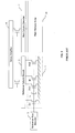
- the device of the present invention comprises an address pad 1, an address buffer 2, an address multiplexer 3, a main row decoder 4, a reference row decoder 5, a reference column decoder 7, a main column decoder 8, a sense amplifier 9, a main memory array 10, a reference array 11, a program circuit 12, a control circuit 13, a pumping circuit 14, a readout pumping circuit 15, a digital/analog converter circuit (D2A) 16, a main high-voltage switch circuit 17, a reference high-voltage switch circuit 18, a first sense data latch circuit 19, a second sense data latch circuit 20, an input/output buffer 21, an I/O pad 22, a command decoder 23, and the like.
- necessary control signals such as a light enable signal, a chip enable signal, an output enable signal and the like (not shown) are supplied to corresponding parts through respective input pads and input buffers.
- the main memory array 10 comprises memory cells having nonvolatile memory elements and arranged in the row direction and the column direction in the form of an array
- the reference array 11 comprises reference memory cells having the same nonvolatile memory elements as the above and arranged similarly.
- each memory cell in the main memory array 10 and the reference array 11 is constituted as flash memory cell comprising a flash memory transistor having a floating gate type of FET structure as a nonvolatile memory element. Therefore, the storage state of the memory cell is set by an amount of electrons stored in the floating gate and its storage state appears as a difference between threshold voltages of the memory transistor.
- the address pad 1 is a terminal for inputting an address signal from the outside, and the address buffer 2 buffers the address signal from the address pad 1 and converts it to an internal signal level.
- the address multiplexer 3 has a function of switching the address signal from the outside to the internal address signal to be used in the internal circuits in various kinds of operation modes and supplies the switched address signal to various kinds of decoders.
- the main row decoder 4 selects the memory cells along the row direction in the main memory array 10
- the reference row decoder 5 selects the reference memory cells along the row direction in the reference array 11.
- the main column decoder 8 selects the memory cells along the column direction in the main memory array 10
- the reference column decoder 7 selects the reference memory cells along the column direction in the reference array 11.
- Each decoder applies a predetermined voltage to each part (a gate, a drain and the like) of the memory cell in the main memory array 10 and the reference memory cell in the reference array 11 in each operation mode (reading, programming and erasing). Therefore, it functions as a part of a readout circuit in a normal readout operation, a program verifying operation and an erase verifying operation.
- the sense amplifier 9 compares a threshold voltage of the memory cell in the main memory array 10, which is selected by the main row decoder 4 and the main column decoder 8 with a threshold voltage of the reference memory cell in the reference array 11, which is selected by the reference row decoder 5 and the reference column decoder 7 to read data programmed in the selected memory cell, and this comprises a well-known circuit. More specifically, the sense amplifier 9 applies the same bias voltage to each gate, source, and drain of both selected memory cell and the reference memory cell, compares the threshold voltage of the selected memory cell with the threshold voltage of the reference memory cell, converts a difference in drain current because of the difference in threshold voltage to a voltage difference, and amplifies the voltage difference. In addition, the sense amplifier 9 is used as a readout circuit at the time of the normal readout and also used as the readout circuit at the time of the program verification and the erase verification in this embodiment.
- the program circuit 12 is a circuit for programming data corresponding to program data inputted through the I/O pad 22 in the selected memory cell, which comprises a conventional circuit constitution.
- the control circuit 13 carries out a program process and an erase process by applying a program pulse and an erase pulse at the time of the program operation and the erase operation, and a verify process to verify a programmed state and an erased state by a predetermined algorithm. More specifically, it comprises a circuit constitution such as a state machine and the like. Therefore, the control circuit 13 functions as a part of a program verification circuit or an erase verification circuit.
- the pumping circuits 14 internally generates a high voltage which is required for the program and erase operations from a power supply voltage supplied from the outside.
- the readout pumping circuit 15 generates an internal power supply voltage which is required for the readout operation from the power supply voltage supplied from the outside. They are needed to lower the power supply voltage and stabilize the internal power supply voltage.
- the digital/analog converter circuit (D2A) 16 drops the internal high voltage generated in the pumping circuit 14 to a voltage level depending on a control signal from the control circuit 13.
- the main high-voltage switch circuit 17 is a voltage selection circuit which selects an appropriate voltage from the voltage supplied from the D2A 16 or the readout pumping circuit 15 so as to correspond to the various kinds of memory operations and supplies it to the main memory array 10.
- the reference high-voltage switch circuit 18 is a voltage selection circuit which selects an appropriate voltage from the voltage supplied from the D2A 16 or the readout pumping circuit 15 so as to correspond to the various kinds of memory operations and supplies it to the reference array.
- the first sense data latch circuit 19 and the second sense data latch circuit 20 temporally store plural bits of data which was read by the sense amplifier 9. When a data width is large, it is divided into two and can be serially outputted.
- the input/output buffer 21 receives the outputs of the first sense data latch circuit 19 and the second sense data latch circuit 20 and outputs them to the outside through the I/O pad 22 at a predetermined output level, and receives the programmed data or another command from the outside through the I/O pad 22.
- the I/O pad 22 is a terminal for inputting and outputting data with the outside.
- the command decoder 23 decodes a command inputted through the input/output buffer 21 and outputs it to the control circuit.
- a class of commands which is used in a general flash memory is assumed, the command is not limited to a particular class of commands.
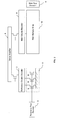
- Fig. 2 is a view schematically showing a relation between a conventional reference array 11 and its peripheral circuits
- Fig. 4 shows kinds of reference memory cells contained in the conventional reference array 11.
- Fig. 3 is a view schematically showing a relation between the reference array 11 of the present invention and its peripheral circuits
- Fig. 5 shows kinds of reference memory cells contained in the reference array 11 of the device of the present invention.
- each memory cell is four-value memory which stores four-value data
- at least seven kinds of reference memory cells are prepared in the conventional example. That is, three kinds of threshold voltages L, M and H are prepared for the normal readout.
- the threshold voltages L, M and H are set at a middle value between an upper limit value of threshold voltage distribution in "11" state (erased state) and a lower limit value of threshold voltage distribution in "10" state, a middle value between an upper limit value of the threshold voltage distribution in the "10” state and a lower limit value of threshold voltage distribution in "01” state, and a middle value between an upper limit value of the threshold voltage distribution in the "01” state and a lower limit value of threshold voltage distribution in "00" state, respectively.
- threshold voltages such as PV1, PV2 and PV3 for program verification.
- the threshold voltages PV1, PV2 and PV3 are set at the lower limit value of the threshold voltage distribution in the "10" state, at the lower limit value of the threshold voltage distribution in the "01” state, and at the lower limit value of the threshold voltage distribution in the "00” state, respectively.
- one kind of threshold voltage EV for erase verification in the conventional reference memory cell is prepared.
- the threshold voltage EV is set at the upper limit value of the threshold voltage distribution in the "11" state (erased state).
- the reference array 11 of the present invention only three kinds of threshold voltages L, M and H for the normal readout are provided and the reference memory cell for the verification is omitted.
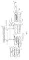
- the reference memory cell corresponding to the program data is selected by the reference column decoder 7 and the reference row decoder 5.
- the reference memory cell having the threshold voltage M is selected while the memory cell to which the data is programmed is selected by the main row decoder 4 and the main column decoder 8. Since the plurality of memory cells are processed at the same time in the program process normally, when their verifications are performed at the same time, the same number of sense amplifiers 9 and the same number of reference memory cells are used. However, the following description will be made for one memory cell.
- a main gate voltage Vmw1 is applied to a gate of the selected memory cell through the main row decoder 4, and a reference gate voltage Vrw1 is applied to a gate of the reference memory cell through the reference row decoder 5.
- each of the gate voltages Vmw1 and Vrw1 is generated by supplying the internal voltage (high voltage) generated in the pumping circuit 14 to the D2A 16 and dividing the internal voltage by a divider circuit comprising a resistance ladder circuit.
- the voltages of 10 mV intervals divided by the ladder resistance for example, can be selected by the selection signal from the control circuit 13.
- the main gate voltage Vmw is set higher than the reference gate voltage Vrw1 by a threshold voltage difference (PV2 - M). Since each of drain currents flowing in the selected memory cell and the reference memory cell is determined by the difference between the gate voltage and the threshold voltage, when the reference gate voltage Vrw1 is lower by the threshold voltage difference (PV2 - M), if it is assumed that the reference gate voltage Vrw1 is raised so as to be the same voltage as the main gate voltage Vmw1, the threshold voltage of the reference memory cell becomes apparently high and equivalent to PV2. Thus, when the threshold voltage of the selected memory cell is less than PV2, the output of the sense amplifier 9 is "1" at the time of the program verification, which is determined that the program process is not completed. Thus, the program pulse is continued to be applied until the threshold voltage of the selected memory cell becomes PV2 or more and the output of the sense amplifier 9 becomes "0".
- the drain currents flowing in the selected memory cell and the reference memory cell are supplied from the readout voltage generation circuit 24 when a predetermined readout voltage generated by the readout generation circuit 24 is lowered to a predetermined bias voltage by a load circuit 25 comprising an N-channel MOSFET, for example, and applied to the drain of the memory cell through the main column decoder 8 and the reference column decoder 7 and the like.
- a load circuit 25 comprising an N-channel MOSFET, for example
- the threshold voltage distribution of the memory cell for programming can be controlled like in the conventional example by adjusting the reference gate voltage Vrw1 without providing the reference memory cell for program verification.
- an operation margin is improved as compared with the conventional example.
- an error of the threshold voltage of the reference memory cell (Cell A) for the readout appears as an error of the substantial threshold voltage of the reference memory cell in the same direction at the time of the verification as it is as shown in Fig. 9.
- the threshold voltage is relatively high at the time of the program verification, even if the threshold voltage of the selected memory cell for the program becomes relatively high, the threshold voltage of the reference memory cell for the normal readout is also shifted to be relatively high, so that the threshold voltage difference between the selected memory cell and the reference memory cell can be maintained.
- the readout operation margin is prevented from being lowered because of the threshold voltage setting error of the reference memory cell for the normal readout, so that the readout operation margin is improved as compared with the conventional example.
- the reference memory cell of the threshold voltage L is selected by the reference column decoder 7 and the reference row decoder 5.
- the memory cell for the erase is selected from erase blocks in the main memory array 10 by the main row decoder 4 and the main column decoder 8 based on an internal address generated in the control circuit 13. Since the memory cell for the erase is erased by the block normally, the verification is performed by the several bits at the same time depending on the number of the sense amplifiers 9. The following description will be made for one selected memory cell.
- the main gate voltage Vmw1 is applied to the gate of the selected memory cell through the main row decoder 4, and a reference gate voltage Vrwle is applied to the gate of the reference memory cell through the reference row decoder 5. While the main gate voltage Vmw1 is set higher than the reference gate voltage Vrw1 by the threshold voltage difference (PV2 - M), for example at the time of the program verification, the main gate voltage Vmw1 is set lower than the reference gate voltage Vrwle by a threshold voltage difference (L - EV) at the time of the erase verification.
- the threshold voltage EV of the reference memory cell for the erase verification is set lower than the threshold voltage L of the reference memory cell for the readout of the data "10" in order to ensure the readout margin.
- the main gate voltage Vmw1 and the reference gate voltage Vrwle are generated by supplying the internal voltage (high voltage) generated in the pumping circuit 14 to the D2A 16 and dividing the interval voltage by a divider circuit comprising the resistance ladder circuit.
- the plural numbers of the reference memory cells having threshold voltages L, M and H for the normal readout are provided depending on constitutions of the main memory array 10 and the reference array 11, a data width, the presence of dual-work function in which while the normal readout operation is performed in a certain memory array block, the program or erase operation can be performed in another memory array block, and their threshold voltages are adjusted (trimmed) by a tester at the time of a test. Therefore, the erase and program operations for the reference memory cell of the reference array 11 can be performed with the circuit for the test. Since the trimming is the same as that for the reference memory cell for the ordinary readout in the conventional flash memory, its description will be omitted.
- one reference memory cell can function as the reference memory cells comprising the plural kinds of the threshold voltages
- one reference memory cell can be used for the readout and the verification.
- one reference memory cell can function as the plural kinds of the reference memory cells for the readout comprising the plural kinds of threshold voltages for the readout.
- one reference memory cell can function as the plural kinds of the reference memory cells for the verification comprising the plural kinds of verifying voltages.
- the number of reference memory cells can be reduced.
- the number of the reference memory cells for the verification is reduced and the labor in the verifying step can be saved.
- an overhead of a layout area for the sense amplifier for reading the storage data in the selected memory cell and the reference memory cell can be reduced.
- the threshold voltage is controlled by the gate input voltage of the reference memory cell, margin voltages of the verifying voltage at the time of readout and the verifying voltage at the time of program or erase can be surely provided, and the operation of the nonvolatile semiconductor memory device can be stabilized, and speeded up, and reliability thereof can be increased.
- the threshold voltage of the reference memory cell can be trimmed with high precision without lowering the production efficiency.
Applications Claiming Priority (2)
| Application Number | Priority Date | Filing Date | Title |
|---|---|---|---|
| JP2004030070A JP2005222625A (ja) | 2004-02-06 | 2004-02-06 | 不揮発性半導体記憶装置 |
| JP2004030070 | 2004-02-06 |
Publications (2)
| Publication Number | Publication Date |
|---|---|
| EP1562200A2 true EP1562200A2 (de) | 2005-08-10 |
| EP1562200A3 EP1562200A3 (de) | 2007-09-05 |
Family
ID=34675541
Family Applications (1)
| Application Number | Title | Priority Date | Filing Date |
|---|---|---|---|
| EP05250628A Withdrawn EP1562200A3 (de) | 2004-02-06 | 2005-02-04 | Nichtflüchtige Halbleiterspeicheranordnung |
Country Status (6)
| Country | Link |
|---|---|
| US (1) | US7020037B2 (de) |
| EP (1) | EP1562200A3 (de) |
| JP (1) | JP2005222625A (de) |
| KR (1) | KR100586680B1 (de) |
| CN (1) | CN1652254A (de) |
| TW (1) | TWI272617B (de) |
Families Citing this family (29)
| Publication number | Priority date | Publication date | Assignee | Title |
|---|---|---|---|---|
| US20060215447A1 (en) * | 2005-03-24 | 2006-09-28 | Beedar Technology Inc. | Asynchronous Memory Array Read/Write Control Circuit |
| US7190621B2 (en) * | 2005-06-03 | 2007-03-13 | Infineon Technologies Ag | Sensing scheme for a non-volatile semiconductor memory cell |
| US7259993B2 (en) * | 2005-06-03 | 2007-08-21 | Infineon Technologies Ag | Reference scheme for a non-volatile semiconductor memory device |
| JP2007012180A (ja) * | 2005-06-30 | 2007-01-18 | Renesas Technology Corp | 半導体記憶装置 |
| EP1750281B1 (de) * | 2005-07-29 | 2011-07-06 | STMicroelectronics Srl | Nichtflüchtiger Halbleiterspeicher mit Referenzzellen und entspechendes Steuerverfahren |
| US8223553B2 (en) * | 2005-10-12 | 2012-07-17 | Macronix International Co., Ltd. | Systems and methods for programming a memory device |
| JP2007128603A (ja) * | 2005-11-04 | 2007-05-24 | Matsushita Electric Ind Co Ltd | メモリ回路 |
| JP4942990B2 (ja) * | 2005-12-12 | 2012-05-30 | パナソニック株式会社 | 半導体記憶装置 |
| US7254071B2 (en) * | 2006-01-12 | 2007-08-07 | Sandisk Corporation | Flash memory devices with trimmed analog voltages |
| US7457178B2 (en) * | 2006-01-12 | 2008-11-25 | Sandisk Corporation | Trimming of analog voltages in flash memory devices |
| US7580288B2 (en) * | 2006-05-24 | 2009-08-25 | Freescale Semiconductor, Inc. | Multi-level voltage adjustment |
| KR100819106B1 (ko) * | 2006-09-27 | 2008-04-02 | 삼성전자주식회사 | 상변화 메모리 장치에서의 라이트 동작방법 |
| US7443753B2 (en) * | 2006-11-21 | 2008-10-28 | Macronix International Co., Ltd. | Memory structure, programming method and reading method therefor, and memory control circuit thereof |
| KR100799018B1 (ko) * | 2006-12-27 | 2008-01-28 | 주식회사 하이닉스반도체 | 불휘발성 메모리 소자 및 자기 보상 방법 |
| KR100837282B1 (ko) * | 2007-06-14 | 2008-06-12 | 삼성전자주식회사 | 비휘발성 메모리 장치, 그것을 포함하는 메모리 시스템,그것의 프로그램 방법 및 읽기 방법 |
| US7663932B2 (en) * | 2007-12-27 | 2010-02-16 | Kabushiki Kaisha Toshiba | Nonvolatile semiconductor memory device |
| US7778098B2 (en) * | 2007-12-31 | 2010-08-17 | Cypress Semiconductor Corporation | Dummy cell for memory circuits |
| JP2009193627A (ja) * | 2008-02-13 | 2009-08-27 | Toshiba Corp | 半導体記憶装置 |
| US7782664B2 (en) * | 2008-05-30 | 2010-08-24 | Freescale Semiconductor, Inc. | Method for electrically trimming an NVM reference cell |
| US8031520B2 (en) * | 2008-08-21 | 2011-10-04 | Macronix International Co., Ltd. | Method for reading and programming a charge-trap memory device compensated for an array/second-bit/neighbor-bit effect |
| JP5295706B2 (ja) * | 2008-10-03 | 2013-09-18 | 株式会社東芝 | 電圧発生回路、及びそれを備えた半導体記憶装置 |
| US8077515B2 (en) * | 2009-08-25 | 2011-12-13 | Micron Technology, Inc. | Methods, devices, and systems for dealing with threshold voltage change in memory devices |
| JPWO2011033701A1 (ja) * | 2009-09-16 | 2013-02-07 | パナソニック株式会社 | 半導体記憶装置 |
| US8248855B2 (en) * | 2010-03-10 | 2012-08-21 | Infinite Memories Ltd. | Method of handling reference cells in NVM arrays |
| US8345483B2 (en) * | 2011-01-21 | 2013-01-01 | Spansion Llc | System and method for addressing threshold voltage shifts of memory cells in an electronic product |
| US8767428B2 (en) * | 2011-06-29 | 2014-07-01 | STMicroelectronics International N. V. | Canary based SRAM adaptive voltage scaling (AVS) architecture and canary cells for the same |
| KR102162701B1 (ko) * | 2013-07-30 | 2020-10-07 | 에스케이하이닉스 주식회사 | 비휘발성 메모리 장치 및 이를 이용하는 반도체 시스템 |
| JP6677383B2 (ja) * | 2015-03-03 | 2020-04-08 | 天馬微電子有限公司 | 電子回路、走査回路及び表示装置並びに電子回路の寿命延長方法 |
| CN113409857B (zh) * | 2021-05-11 | 2024-04-05 | 珠海博雅科技股份有限公司 | 参考单元替换方法、装置及存储介质 |
Citations (4)
| Publication number | Priority date | Publication date | Assignee | Title |
|---|---|---|---|---|
| US6301156B1 (en) * | 1999-11-09 | 2001-10-09 | Fujitsu Limited | Nonvolatile semiconductor memory device |
| US20020036925A1 (en) * | 2000-09-22 | 2002-03-28 | Toru Tanzawa | Non-volatile semiconductor memory |
| US20020071313A1 (en) * | 2000-12-11 | 2002-06-13 | Kabushiki Kaisha Toshiba | Non-volatile semiconductor memory device |
| US6580644B1 (en) * | 2001-05-31 | 2003-06-17 | Samusung Electronics Co., Ltd. | Flash memory device capable of checking memory cells for failure characteristics |
Family Cites Families (2)
| Publication number | Priority date | Publication date | Assignee | Title |
|---|---|---|---|---|
| JPS59104796A (ja) | 1982-12-03 | 1984-06-16 | Mitsubishi Electric Corp | 不揮発性半導体メモリ装置 |
| WO1997048099A1 (en) * | 1996-06-14 | 1997-12-18 | Siemens Aktiengesellschaft | A device and method for multi-level charge/storage and reading out |
-
2004
- 2004-02-06 JP JP2004030070A patent/JP2005222625A/ja active Pending
-
2005
- 2005-02-03 KR KR1020050009917A patent/KR100586680B1/ko not_active IP Right Cessation
- 2005-02-04 TW TW094103534A patent/TWI272617B/zh not_active IP Right Cessation
- 2005-02-04 EP EP05250628A patent/EP1562200A3/de not_active Withdrawn
- 2005-02-04 US US11/051,139 patent/US7020037B2/en not_active Expired - Fee Related
- 2005-02-06 CN CNA2005100078717A patent/CN1652254A/zh active Pending
Patent Citations (4)
| Publication number | Priority date | Publication date | Assignee | Title |
|---|---|---|---|---|
| US6301156B1 (en) * | 1999-11-09 | 2001-10-09 | Fujitsu Limited | Nonvolatile semiconductor memory device |
| US20020036925A1 (en) * | 2000-09-22 | 2002-03-28 | Toru Tanzawa | Non-volatile semiconductor memory |
| US20020071313A1 (en) * | 2000-12-11 | 2002-06-13 | Kabushiki Kaisha Toshiba | Non-volatile semiconductor memory device |
| US6580644B1 (en) * | 2001-05-31 | 2003-06-17 | Samusung Electronics Co., Ltd. | Flash memory device capable of checking memory cells for failure characteristics |
Also Published As
| Publication number | Publication date |
|---|---|
| JP2005222625A (ja) | 2005-08-18 |
| EP1562200A3 (de) | 2007-09-05 |
| TW200537511A (en) | 2005-11-16 |
| TWI272617B (en) | 2007-02-01 |
| KR100586680B1 (ko) | 2006-06-08 |
| CN1652254A (zh) | 2005-08-10 |
| KR20060045318A (ko) | 2006-05-17 |
| US20050174868A1 (en) | 2005-08-11 |
| US7020037B2 (en) | 2006-03-28 |
Similar Documents
| Publication | Publication Date | Title |
|---|---|---|
| US7020037B2 (en) | Nonvolatile semiconductor memory device | |
| JP4187197B2 (ja) | 半導体メモリ装置の制御方法 | |
| US10032517B2 (en) | Memory architecture having two independently controlled voltage pumps | |
| KR100903839B1 (ko) | 불휘발성 반도체 메모리 및 그 동작 방법 | |
| KR100828196B1 (ko) | 플래시 메모리 어레이의 코어 셀들의 소프트 프로그램 및소프트 프로그램 검증 | |
| US7116581B2 (en) | Nonvolatile semiconductor memory device and method of programming in nonvolatile semiconductor memory device | |
| US8213232B2 (en) | Nonvolatile semiconductor memory, method for reading out thereof, and memory card | |
| JP4262227B2 (ja) | 半導体記憶装置の読み出し回路 | |
| KR100501962B1 (ko) | 전기적으로프로그램가능한메모리및프로그래밍방법 | |
| KR20060064856A (ko) | 불휘발성 메모리 장치의 프로그램 검증방법 | |
| EP0992998B1 (de) | Nichtflüchtige Speicheranordnung und Verfahren zu ihrer Prüfung | |
| JP2005535062A (ja) | 多重レベルメモリセル状態を検知するための参照レベルを設定する方法 | |
| US6829173B2 (en) | Semiconductor memory device capable of accurately writing data | |
| US6185131B1 (en) | Nonvolatile semiconductor storage device capable of electrically isolating dummy cell array region from memory cell array region | |
| US7110300B2 (en) | Method of programming a multi-level, electrically programmable non-volatile semiconductor memory | |
| US8576630B2 (en) | Non-volatile memory device with plural reference cells, and method of setting the reference cells | |
| JP2008130182A (ja) | 不揮発性半導体記憶装置 | |
| US6934185B2 (en) | Programming method for non volatile multilevel memory cells and corresponding programming circuit | |
| US7924627B2 (en) | Semiconductor memory device | |
| KR101035580B1 (ko) | 플래시 메모리 장치의 기준 셀 트리밍 방법 | |
| JP3133675B2 (ja) | 半導体記憶装置 | |
| JPH11126487A (ja) | 不揮発性半導体メモリ | |
| JP4004527B2 (ja) | 多状態eepromの読み書き回路 | |
| JP3828900B2 (ja) | 多状態eepromの電荷読み書きシステムおよび読み出し方法 |
Legal Events
| Date | Code | Title | Description |
|---|---|---|---|
| PUAI | Public reference made under article 153(3) epc to a published international application that has entered the european phase |
Free format text: ORIGINAL CODE: 0009012 |
|
| AK | Designated contracting states |
Kind code of ref document: A2 Designated state(s): AT BE BG CH CY CZ DE DK EE ES FI FR GB GR HU IE IS IT LI LT LU MC NL PL PT RO SE SI SK TR |
|
| AX | Request for extension of the european patent |
Extension state: AL BA HR LV MK YU |
|
| PUAL | Search report despatched |
Free format text: ORIGINAL CODE: 0009013 |
|
| AK | Designated contracting states |
Kind code of ref document: A3 Designated state(s): AT BE BG CH CY CZ DE DK EE ES FI FR GB GR HU IE IS IT LI LT LU MC NL PL PT RO SE SI SK TR |
|
| AX | Request for extension of the european patent |
Extension state: AL BA HR LV MK YU |
|
| RIC1 | Information provided on ipc code assigned before grant |
Ipc: G11C 16/34 20060101ALI20070802BHEP Ipc: G11C 11/56 20060101ALI20070802BHEP Ipc: G11C 16/28 20060101AFI20050527BHEP |
|
| 17P | Request for examination filed |
Effective date: 20071114 |
|
| 17Q | First examination report despatched |
Effective date: 20080303 |
|
| AKX | Designation fees paid |
Designated state(s): DE FR GB IT |
|
| STAA | Information on the status of an ep patent application or granted ep patent |
Free format text: STATUS: THE APPLICATION IS DEEMED TO BE WITHDRAWN |
|
| 18D | Application deemed to be withdrawn |
Effective date: 20080715 |