EP1560792B1 - Herstellung einer kohlenstoffnanoröhrchenvorrichtung - Google Patents
Herstellung einer kohlenstoffnanoröhrchenvorrichtung Download PDFInfo
- Publication number
- EP1560792B1 EP1560792B1 EP03816306.9A EP03816306A EP1560792B1 EP 1560792 B1 EP1560792 B1 EP 1560792B1 EP 03816306 A EP03816306 A EP 03816306A EP 1560792 B1 EP1560792 B1 EP 1560792B1
- Authority
- EP
- European Patent Office
- Prior art keywords
- carbon nanotube
- substrate
- aperture
- catalyst
- contact pads
- Prior art date
- Legal status (The legal status is an assumption and is not a legal conclusion. Google has not performed a legal analysis and makes no representation as to the accuracy of the status listed.)
- Expired - Lifetime
Links
Images


Classifications
-
- H—ELECTRICITY
- H10—SEMICONDUCTOR DEVICES; ELECTRIC SOLID-STATE DEVICES NOT OTHERWISE PROVIDED FOR
- H10K—ORGANIC ELECTRIC SOLID-STATE DEVICES
- H10K19/00—Integrated devices, or assemblies of multiple devices, comprising at least one organic element specially adapted for rectifying, amplifying, oscillating or switching, covered by group H10K10/00
- H10K19/10—Integrated devices, or assemblies of multiple devices, comprising at least one organic element specially adapted for rectifying, amplifying, oscillating or switching, covered by group H10K10/00 comprising field-effect transistors
-
- B—PERFORMING OPERATIONS; TRANSPORTING
- B82—NANOTECHNOLOGY
- B82Y—SPECIFIC USES OR APPLICATIONS OF NANOSTRUCTURES; MEASUREMENT OR ANALYSIS OF NANOSTRUCTURES; MANUFACTURE OR TREATMENT OF NANOSTRUCTURES
- B82Y10/00—Nanotechnology for information processing, storage or transmission, e.g. quantum computing or single electron logic
-
- B—PERFORMING OPERATIONS; TRANSPORTING
- B82—NANOTECHNOLOGY
- B82Y—SPECIFIC USES OR APPLICATIONS OF NANOSTRUCTURES; MEASUREMENT OR ANALYSIS OF NANOSTRUCTURES; MANUFACTURE OR TREATMENT OF NANOSTRUCTURES
- B82Y30/00—Nanotechnology for materials or surface science, e.g. nanocomposites
-
- B—PERFORMING OPERATIONS; TRANSPORTING
- B82—NANOTECHNOLOGY
- B82Y—SPECIFIC USES OR APPLICATIONS OF NANOSTRUCTURES; MEASUREMENT OR ANALYSIS OF NANOSTRUCTURES; MANUFACTURE OR TREATMENT OF NANOSTRUCTURES
- B82Y40/00—Manufacture or treatment of nanostructures
-
- C—CHEMISTRY; METALLURGY
- C01—INORGANIC CHEMISTRY
- C01B—NON-METALLIC ELEMENTS; COMPOUNDS THEREOF; METALLOIDS OR COMPOUNDS THEREOF NOT COVERED BY SUBCLASS C01C
- C01B3/00—Hydrogen; Gaseous mixtures containing hydrogen; Separation of hydrogen from mixtures containing it; Purification of hydrogen
- C01B3/02—Production of hydrogen or of gaseous mixtures containing a substantial proportion of hydrogen
- C01B3/22—Production of hydrogen or of gaseous mixtures containing a substantial proportion of hydrogen by decomposition of gaseous or liquid organic compounds
- C01B3/24—Production of hydrogen or of gaseous mixtures containing a substantial proportion of hydrogen by decomposition of gaseous or liquid organic compounds of hydrocarbons
- C01B3/26—Production of hydrogen or of gaseous mixtures containing a substantial proportion of hydrogen by decomposition of gaseous or liquid organic compounds of hydrocarbons using catalysts
-
- C—CHEMISTRY; METALLURGY
- C01—INORGANIC CHEMISTRY
- C01B—NON-METALLIC ELEMENTS; COMPOUNDS THEREOF; METALLOIDS OR COMPOUNDS THEREOF NOT COVERED BY SUBCLASS C01C
- C01B32/00—Carbon; Compounds thereof
- C01B32/15—Nano-sized carbon materials
- C01B32/158—Carbon nanotubes
- C01B32/16—Preparation
- C01B32/162—Preparation characterised by catalysts
-
- H—ELECTRICITY
- H10—SEMICONDUCTOR DEVICES; ELECTRIC SOLID-STATE DEVICES NOT OTHERWISE PROVIDED FOR
- H10K—ORGANIC ELECTRIC SOLID-STATE DEVICES
- H10K10/00—Organic devices specially adapted for rectifying, amplifying, oscillating or switching; Organic capacitors or resistors having potential barriers
- H10K10/20—Organic diodes
- H10K10/23—Schottky diodes
-
- H—ELECTRICITY
- H10—SEMICONDUCTOR DEVICES; ELECTRIC SOLID-STATE DEVICES NOT OTHERWISE PROVIDED FOR
- H10K—ORGANIC ELECTRIC SOLID-STATE DEVICES
- H10K10/00—Organic devices specially adapted for rectifying, amplifying, oscillating or switching; Organic capacitors or resistors having potential barriers
- H10K10/40—Organic transistors
- H10K10/46—Field-effect transistors, e.g. organic thin-film transistors [OTFT]
-
- H—ELECTRICITY
- H10—SEMICONDUCTOR DEVICES; ELECTRIC SOLID-STATE DEVICES NOT OTHERWISE PROVIDED FOR
- H10K—ORGANIC ELECTRIC SOLID-STATE DEVICES
- H10K85/00—Organic materials used in the body or electrodes of devices covered by this subclass
- H10K85/20—Carbon compounds, e.g. carbon nanotubes or fullerenes
- H10K85/221—Carbon nanotubes
-
- B—PERFORMING OPERATIONS; TRANSPORTING
- B01—PHYSICAL OR CHEMICAL PROCESSES OR APPARATUS IN GENERAL
- B01J—CHEMICAL OR PHYSICAL PROCESSES, e.g. CATALYSIS OR COLLOID CHEMISTRY; THEIR RELEVANT APPARATUS
- B01J23/00—Catalysts comprising metals or metal oxides or hydroxides, not provided for in group B01J21/00
- B01J23/70—Catalysts comprising metals or metal oxides or hydroxides, not provided for in group B01J21/00 of the iron group metals or copper
-
- B—PERFORMING OPERATIONS; TRANSPORTING
- B01—PHYSICAL OR CHEMICAL PROCESSES OR APPARATUS IN GENERAL
- B01J—CHEMICAL OR PHYSICAL PROCESSES, e.g. CATALYSIS OR COLLOID CHEMISTRY; THEIR RELEVANT APPARATUS
- B01J37/00—Processes, in general, for preparing catalysts; Processes, in general, for activation of catalysts
- B01J37/02—Impregnation, coating or precipitation
- B01J37/0238—Impregnation, coating or precipitation via the gaseous phase-sublimation
-
- C—CHEMISTRY; METALLURGY
- C01—INORGANIC CHEMISTRY
- C01B—NON-METALLIC ELEMENTS; COMPOUNDS THEREOF; METALLOIDS OR COMPOUNDS THEREOF NOT COVERED BY SUBCLASS C01C
- C01B2202/00—Structure or properties of carbon nanotubes
- C01B2202/02—Single-walled nanotubes
-
- C—CHEMISTRY; METALLURGY
- C01—INORGANIC CHEMISTRY
- C01B—NON-METALLIC ELEMENTS; COMPOUNDS THEREOF; METALLOIDS OR COMPOUNDS THEREOF NOT COVERED BY SUBCLASS C01C
- C01B2202/00—Structure or properties of carbon nanotubes
- C01B2202/06—Multi-walled nanotubes
-
- C—CHEMISTRY; METALLURGY
- C01—INORGANIC CHEMISTRY
- C01B—NON-METALLIC ELEMENTS; COMPOUNDS THEREOF; METALLOIDS OR COMPOUNDS THEREOF NOT COVERED BY SUBCLASS C01C
- C01B2202/00—Structure or properties of carbon nanotubes
- C01B2202/20—Nanotubes characterized by their properties
- C01B2202/22—Electronic properties
-
- C—CHEMISTRY; METALLURGY
- C01—INORGANIC CHEMISTRY
- C01B—NON-METALLIC ELEMENTS; COMPOUNDS THEREOF; METALLOIDS OR COMPOUNDS THEREOF NOT COVERED BY SUBCLASS C01C
- C01B2203/00—Integrated processes for the production of hydrogen or synthesis gas
- C01B2203/02—Processes for making hydrogen or synthesis gas
- C01B2203/0266—Processes for making hydrogen or synthesis gas containing a decomposition step
- C01B2203/0277—Processes for making hydrogen or synthesis gas containing a decomposition step containing a catalytic decomposition step
-
- C—CHEMISTRY; METALLURGY
- C01—INORGANIC CHEMISTRY
- C01B—NON-METALLIC ELEMENTS; COMPOUNDS THEREOF; METALLOIDS OR COMPOUNDS THEREOF NOT COVERED BY SUBCLASS C01C
- C01B2203/00—Integrated processes for the production of hydrogen or synthesis gas
- C01B2203/10—Catalysts for performing the hydrogen forming reactions
- C01B2203/1041—Composition of the catalyst
- C01B2203/1047—Group VIII metal catalysts
- C01B2203/1052—Nickel or cobalt catalysts
-
- C—CHEMISTRY; METALLURGY
- C01—INORGANIC CHEMISTRY
- C01B—NON-METALLIC ELEMENTS; COMPOUNDS THEREOF; METALLOIDS OR COMPOUNDS THEREOF NOT COVERED BY SUBCLASS C01C
- C01B2203/00—Integrated processes for the production of hydrogen or synthesis gas
- C01B2203/12—Feeding the process for making hydrogen or synthesis gas
- C01B2203/1205—Composition of the feed
- C01B2203/1211—Organic compounds or organic mixtures used in the process for making hydrogen or synthesis gas
- C01B2203/1235—Hydrocarbons
- C01B2203/1241—Natural gas or methane
-
- H—ELECTRICITY
- H01—ELECTRIC ELEMENTS
- H01J—ELECTRIC DISCHARGE TUBES OR DISCHARGE LAMPS
- H01J2201/00—Electrodes common to discharge tubes
- H01J2201/30—Cold cathodes
- H01J2201/304—Field emission cathodes
- H01J2201/30446—Field emission cathodes characterised by the emitter material
- H01J2201/30453—Carbon types
- H01J2201/30469—Carbon nanotubes (CNTs)
-
- Y—GENERAL TAGGING OF NEW TECHNOLOGICAL DEVELOPMENTS; GENERAL TAGGING OF CROSS-SECTIONAL TECHNOLOGIES SPANNING OVER SEVERAL SECTIONS OF THE IPC; TECHNICAL SUBJECTS COVERED BY FORMER USPC CROSS-REFERENCE ART COLLECTIONS [XRACs] AND DIGESTS
- Y10—TECHNICAL SUBJECTS COVERED BY FORMER USPC
- Y10T—TECHNICAL SUBJECTS COVERED BY FORMER US CLASSIFICATION
- Y10T428/00—Stock material or miscellaneous articles
- Y10T428/24—Structurally defined web or sheet [e.g., overall dimension, etc.]
- Y10T428/24273—Structurally defined web or sheet [e.g., overall dimension, etc.] including aperture
- Y10T428/24322—Composite web or sheet
- Y10T428/24331—Composite web or sheet including nonapertured component
Definitions
- This invention relates generally to carbon nanotube devices and to the fabrication of such devices.
- carbon nanotubes have attracted intense research into their electrical and mechanical properties and have been proposed for implementation in a wide range of electronics as well as mechanical and electromechanical applications.
- carbon nanotubes are distinctly well-suited for applications including, e.g., microelectronic and nanoelectronic devices and systems, chemical sensors, transducers, displays, physical probes, and energy storage devices.
- Synthesis of carbon nanotubes has been achieved by various techniques, including, e.g., methods of arc-discharge, laser ablation, and thermal decomposition of a hydrocarbon. There has been demonstrated with such methods the ability to produce a range of nanotube characteristics. For example, there can be produced films, or mats, of randomly oriented nanotubes or alternatively, arrays of nanotubes that are aligned in a selected orientation. There has also been demonstrated the ability to selectively produce single-walled nanotubes (SWNTs) or multi-walled nanotubes (MWNTs) as-desired for a given application.
- SWNTs single-walled nanotubes
- MWNTs multi-walled nanotubes
- nanotubes As the applications for carbon nanotubes present more particular requirements, additional precision in the control of nanotube synthesis is critical. Specifically, precise and repeatable control of nanotube location, orientation, diameter, and single- or multi-wall configuration are required to successfully address many important applications. Without such control, nanotubes cannot meet the commercial manufacturing requirements of applications for which nanotubes are so well suited.
- a carbon nanotube device in accordance with the invention includes a support structure including an aperture extending from a front surface to a back surface of the structure as disclosed in claim 1 . At least one carbon nanotube extends across the aperture and is accessible through the aperture from both the front surface and the back surface of the support structure. With this arrangement, the nanotube can be employed in a wide range of applications for which there is required exposure of the nanotube to an environment of interest.
- a gas or liquid of interest can be directed through the support structure aperture to enable sensing or other function by the nanotube as the gas or liquid passes around the nanotube.
- these configurations can be used directly in nano-electromechanical applications, such as high frequency resonators.
- the carbon nanotube provided in the carbon nanotube device of the invention can be a single-walled carbon nanotube, a multi-walled nanotube, and either a semiconducting or metallic nanotube, and can be provided as a plurality of nanotubes.
- the support structure can be provided as a substrate, e.g., a semiconducting substrate, a membrane, e.g., a nitride or oxide membrane, or other suitable structure. Whatever support structure is provided, it can be aligned between a source of electrons and an electron detector for transmission electron microscopy of the carbon nanotube. At least one pair of electrically conducting contact pads disposed on the support structure separated by the aperture are provided. A plurality of pairs of contact pads can be disposed at locations around the aperture.
- a carbon nanotube device can be fabricated by the method disclosed in claim 24.
- the carbon nanotube catalyst region is formed by vapor depositing, e.g., by thermal evaporation, a catalyst material, such as Fe, and lithographically patterning the deposited catalyst material to define the catalyst region.
- a catalyst region of less than about 2 nm in thickness can be preferred for enabling selective synthesis of single-walled nanotubes, and pairs of catalyst regions can be formed if desired.
- An electrically conducting contact pad is provided under the carbon nanotube catalyst region on the support structure surface.
- a contact pad can be formed by, e.g., depositing a layer of metal and etching the metal layer to form a contact pad prior to forming a catalyst region on the contact pad.
- the hydrocarbon gas to which the catalyst region is exposed can be substantially only methane, supplied at a flow rate of, e.g., less than about 400 sccm.
- the methane exposure can be carried out at a temperature of, e.g., less than about 1500 °C.
- an electric field can be applied across the aperture in a direction corresponding to a desired nanotube synthesis direction.
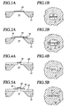
- a nanotube 10 in a first nanotube device in accordance with the invention, there is provided a nanotube 10 the ends of which contact a support structure such as a substrate 12 having an aperture 14 across which the single-walled nanotube extends.
- a support structure such as a substrate 12 having an aperture 14 across which the single-walled nanotube extends.
- the aperture 14 extends completely through the substrate 12 the nanotube forms a bridge across the aperture and can be accessed from either face of the substrate.
- the substrate aperture 14 is shown in this example as being square, such is not specifically required; the aperture can be provided as any convenient shape, e.g., circular, rectangular, or other suitable shape.
- this suspended nanotube configuration can be employed in accordance with the invention to make electrical contact between two electrodes or electrically conducting regions on the substrate.
- electrical contact pads 16 are provided atop a substrate 12 having an aperture 14 across which a nanotube extends.
- the nanotube 10 makes a bridging contact between the two electrodes across the aperture in the substrate 12.
- the nanotube is synthesized, by the process described below, to be located on top of the contact pads.
- contact pads 16 at opposite ends of the aperture 12 such is not specifically required; contact pads can be provided at other locations around the periphery of the aperture and can be provided as groups of three or more electrodes as suitable for a given application.
- the invention provides the ability to produce selected arrangements of nanotubes on a substrate in various nanotube device configurations.
- a common feature of all arrangements provided by the invention is an aperture or other configuration in a support substrate which enables access to the nanotube from both sides of the substrate.
- the nanotube thereby forms a bridge across the substrate aperture.
- the nanotube can be employed in a wide range of applications for which there is required exposure of the nanotube to an environment of interest.
- a gas or liquid of interest can be directed through the substrate aperture to enable sensing or other function by the nanotube as the gas or liquid passes around the nanotube.
- these configurations can be used directly in nano-electromechanical applications, such as high frequency resonators.
- the suspended nanotube arrangement provided by the invention enables in situ examination and test of a synthesized nanotube in a particularly convenient manner. It is now common practice to examine synthesized nanotubes by transmission electron microscopy (TEM) to determine the nanotube diameter, wall thickness, and single- or multi-wall configuration of the nanotube. In general, TEM requires the ability to configure a nanotube under investigation between an electron beam source and a detector. With the arrangement of the invention, a synthesized nanotube as-grown on a substrate can be examined in situ, without the need for destructive nanotube removal or physical interference.
- TEM transmission electron microscopy
- a substrate 12 having a nanotube suspended across an aperture 14 in the substrate can be positioned between an electron beam source 15 and a detector 17, i.e., with the aperture 14 in the electron beam path to the detector 17.
- Trajectory of the electron beam through the nanotube 10 and through the substrate aperture 14 to the detector enables TEM analysis of the nanotube in situ, i.e., at its synthesized, intended location on the substrate. It is generally recognized that nm-scale TEM resolution is required to enable sufficient precision in nanotube analysis.
- the substrate aperture configuration provided by the invention enables such TEM resolution with a substrate arrangement that is easily positioned for analysis without destruction of a nanotube under investigation.
- the invention contemplates a wide range of alternative structures in which an aperture can be provided for enabling a suspended nanotube configuration.
- an aperture 14 in a membrane 18 that is disposed on a surface of a substrate 12.
- the nanotube 10 is provided across the aperture in the membrane.
- the cross sectional view of Fig. 4A is not shown to scale for clarity; the membrane thickness can be of a selected suitable thickness, and the substrate need not be of a specific thickness.
- Figs. 5A-5B as in the substrate configuration of Figs. 2A-2B , there can here be provided electrically conductive contact pads or strips 16 at peripheral locations around the aperture 14 in the membrane 18.
- the suspended nanotube 10 then is configured to bridge the contact pads across the aperture.
- the substrate can be provided as any suitable material and can consist of multiple composite material layers.
- a substrate surface membrane can be provided as any suitable material and can consist of multiple membrane material layers as-required for a given application.
- the electrically conducting contact pads or strips can be provided of any suitable conducting material that is compatible with the nanotube synthesis process, as described below, to enable formation of a nanotube that is disposed on top of the pad, i.e., that contacts the top surface of the contact pad or strip. There is no required pad shape or pattern, but an edge of each contact pad coincides with the periphery of the aperture across which a nanotube is to be synthesized.
- the contact pads can make electrical connection to circuitry that is provided on the substrate or to locations for connection with external circuitry. Indeed, the contact pads are shown in the figures as isolated structures only for clarity; it is understood in accordance with the invention that the contact pads can be provided in a range of configurations to make connection to other circuits and/or devices.
- Figs. 1A-4B illustrate a single nanotube for clarity, but in accordance with the invention, multiple nanotubes can be provided across a single aperture and between multiple contact pads.
- Fig. 6 an example configuration of such is shown, with several nanotubes 10 spanning an aperture 14 in a substrate 12.
- arrays of nanotubes and/or bundles of nanotubes can be provided across an aperture between multiple pairs of contact pads, and can make contact between several pads.
- contact pads can be located at various points around the aperture periphery, with nanotubes connecting a variety of the pads.
- electric fields can be applied selectively between particular contact pads to direct the growth of nanotubes between designated contact pads.
- the nanotube configurations of Figs. 1A-2B and Figs. 4A-5B can be fabricated by any suitable synthesis process that accommodates production of an aperture in a structure that is to support the nanotubes and preferably in addition to support electrical contact pads to which the nanotubes are connected.
- the invention provides a process sequence that can be particularly advantageous for controllably producing single-walled nanotubes that span an aperture in a support structure. While this example process described below can be preferred for many applications, it is to be recognized that other fabrication processes and nanotube synthesis techniques can also be employed.
- a substrate 12 of a selected material e.g., silicon, alumina, sapphire, or other selected material.
- the selected substrate material preferably is not deleteriously affected by the nanotube synthesis temperature, and preferably does not diffuse into layers that may be applied to the substrate. If a membrane is to be fabricated on the substrate, then a membrane layer 19 is formed, on the front surface of the substrate, and e.g., a corresponding layer 21 is also formed on the back substrate surface.
- a membrane layer of silicon nitride or silicon dioxide e.g., of about 500 nm in thickness, can be formed on both silicon substrate surfaces in the conventional manner, e.g., by low pressure chemical vapor deposition (LPCVD).
- LPCVD low pressure chemical vapor deposition
- a region of the membrane layer 21 on the back substrate surface is then patterned and etched, e.g., by reactive ion etching, to remove a portion of the membrane layer 21 to expose the substrate surface for production of a suspended membrane at the front surface of the substrate.
- the substrate is then etched through its thickness to the membrane layer 19 at the front surface of the substrate to produce a freestanding membrane; for many applications, a membrane extent of, e.g., about 100 ⁇ m can be suitable.
- silicon etch techniques e.g., anisotropic wet etching by KOH, can be employed in the conventional manner.
- the backside layer 21 can be removed if desired. If a substrate is to be employed without a membrane layer, then the formation of membrane layers 19, 21 is not required, and bulk etching of the substrate is preferably carried out to form a thinned substrate front surface region at the location corresponding to the membrane layer 19.
- one or more metal layers can be deposited for forming electrically conducting contact pads on the substrate or membrane surface, if contact pads are desired for a given application.
- Patterning of the metal contact pad layer can be carried out using a photoresist lift-off process or other suitable technique.
- a photoresist layer 20 can be deposited and patterned and metal layer or layers 22, 24, blanket-deposited over the patterned photoresist.
- the patterned photoresist layer 20 preferably defines the contact pad areas and a central area 21 that is between the contact pad locations and is the location at which the aperture is to be formed. For many applications, it can be preferred for the contact pads to extend several microns or less.
- a layer of Cr is deposited as a first metal layer 22, of, e.g., about 15 - 50 nm in thickness, to serve as an adhesion layer, and a metal electrode material layer of Pt of, e.g., about 50 nm in thickness is then deposited as a second metal layer 24.
- a metal electrode material layer of Pt of, e.g., about 50 nm in thickness is then deposited as a second metal layer 24.
- Any suitable metal or composite of metals can be employed, so long as the selected material can withstand a subsequent heat cycle for nanotube synthesis. Conventional metal electroplating processes, or other selected metal deposition process can be employed.
- the metal layers are deposited on a membrane 18. It is preferred in accordance with the invention that the membrane material be electrically insulating such that the metal contact pads are discretely electrically isolated. Similarly, if a substrate surface itself, rather than a membrane, is to be employed for nanotube synthesis, then the substrate surface preferably is electrically insulating. Given a semiconducting substrate of, e.g., silicon, or a membrane material of, e.g., silicon or polysilicon, it can be preferred to provide this condition with an insulating layer, e.g., of silicon dioxide or silicon nitride, on the substrate or membrane surface prior to metal contact pad formation.
- an insulating layer e.g., of silicon dioxide or silicon nitride
- the nanotube catalyst layer can be formed in any convenient manner, of a suitable material.
- a nanotube catalyst of layer of, e.g., Fe, Co, Ni, or alloys of such are understood to be most effective for many applications.
- the invention provides a preferred catalyst deposition process that is understood to enable precise control of catalyst properties, and correspondingly precise control of nanotube growth, such that single-walled nanotubes oriented horizontally, parallel to a support surface, are selectively synthesized.
- the catalyst layer is formed by vapor deposition of a solid catalyst material, by sputtering, molecular beam epitaxy, sol gel formation, E-beam evaporation, thermal evaporation, or other selected vapor deposition process.
- Whatever vapor deposition process is selected, it preferably is controlled to enable very low coverage of the vapor-deposited film, such that no more than several monolayers of the selected catalyst material are deposited on the membrane or support substrate.
- thermal evaporation of Fe using a tungsten boat spot welded with Fe foil can be carried out under vacuum conditions, e.g., at a pressure of about 10 -5 or 10 -6 Torr, to produce a Fe catalyst layer of selected thickness.
- the resulting catalyst layer thickness be less than about 2 nm, or considered another way, it is preferred that the catalyst layer be characterized by a layer coverage of about 17 x 10 15 atoms/cm 2 or less. It is understood that as the catalyst layer thickness is increased, the diameter of nanotubes that are horizontally synthesized from the catalyst layer correspondingly increases, and above a threshold catalyst layer thickness, multi-walled, rather than single-walled, horizontal nanotubes are formed.
- the invention provides the specification of a thin catalyst layer, e.g., of 2 nm in thickness or less, for predictably and reliably forming single-walled nanotubes. If a given application does not absolutely require the production of single-walled nanotubes, then the thickness of the catalyst layer is not critical, but it is to be recognized that above a critical thickness, the catalyst layer will not support synthesis of horizontal nanotubes, and thus, to ensure horizontal nanotube synthesis across an aperture in accordance with the invention, a relatively thin catalyst layer can be preferred.
- a catalyst layer 26 is formed on top of a metal layer or layers 22, 24, then by using lift-off techniques, the patterned photoresist layer 20 is removed, resulting in patterned catalyst/electrode regions.
- This technique can be particularly advantageous because it enables patterning of both electrode and catalyst layers in a single step.
- an additional lithographic and etch sequence can be carried out to remove catalyst material from portions of the contact layer.
- the catalyst layer is masked with, e.g., a patterned photoresist layer, exposing regions of the catalyst layer that are to be removed.
- a dry etch process e.g., plasma etching, ion beam etching, or other technique, is then employed to remove the unwanted catalyst layer regions. It is recognized that many catalyst layer etch processes may not be significantly selective in etching the catalyst material over the underlying metal electrode material. It therefore can be preferred that the catalyst etch process be controlled as a timed process or with other controls to ensure that the integrity of the metal contact pad material is maintained.
- the catalyst layer can be patterned and etched in a sequence of steps separate from that employed for the electrode layer.
- the electrode layer can be patterned by, e.g., a lift-off process as just described, and then the catalyst layer deposited and patterned by a second separate lift-off process.
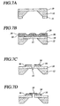
- a photoresist layer 28 is formed over the produced contact pads 16 and the designated location for the aperture and patterned to expose regions of the contact pads at which it is desired to provide a region of nanotube catalyst layer.
- the catalyst layer 26 is then blanket-deposited, preferably by a selected vapor deposition process like that described above.
- lift-off of the photoresist layer 28 is then carried out to remove portions of the catalyst layer, resulting in a patterned catalyst region atop the contact pads.
- the catalyst layer be patterned by a lift-off process; instead, the catalyst layer can be blanket-deposited on the contact pads and then etched, e.g., by lithographic patterning of a photoresist layer applied on top of the catalyst layer and patterned to define distinct catalyst islands. Etching of the catalyst regions exposed through the photoresist pattern can then be carried out employing a suitable etch process.
- This approach like the catalyst lift-off approach, has the advantage of enabling precise formation of catalyst islands that do not necessarily extend across an entire electrode contact pad, and therefore that more precisely define the location of nanotube synthesis.
- the contact pad and catalyst regions can be extended across an intended aperture location, such that production of an aperture through the contact pad and catalyst layers enables self alignment of the contact pads and catalyst regions with edges of the aperture.
- Fig. 9 provides a planar view of one example of such a preferred structure, with two contact pads 16 separated by the aperture 14, with the contact pads abutting the edge 32 of the aperture.
- This illustrated structure can be formed in any suitable manner, and the invention is not limited to a particular technique for producing this structure. Any convenient process that enables alignment of catalyst regions and contact pads with edges of an aperture can be employed.
- a condition in which catalyst layer regions 26 abut the aperture edge 32 and do not extend across the expanse of the contact pads is also shown in the configuration of Fig. 9 .
- Such a condition can be produced by the various catalyst layer etch sequences just described.
- Whatever catalyst pattern is desired, it is preferably produced in accordance with the invention by a lithographic process that enables precise definition of the location and extent of catalyst regions. This lithographic catalyst definition, in combination with vapor deposition of a thin catalyst layer, enables precise nanotube synthesis.
- this preferable lithographic definition of the catalyst regions does not require etching of the catalyst layer.
- a blanket deposition of catalyst layer 26 can be carried out in the manner described above, and then a capping layer 34 can be deposited and patterned.
- the capping layer pattern exposes regions of the catalyst layer at which it is desired to synthesize nanotubes, with the remainder of the catalyst layer being covered to inhibit nanotube synthesis.
- the catalyst layer is not itself etched, but through lithography the precise location of catalyst exposure for nanotube synthesis is accomplished.
- an aperture is formed through the membrane 18 or other support structure on which nanotubes are to be provided.
- the membrane or substrate is lithographically masked and then etched with a suitable etchant, e.g., a plasma etch, with the adjacent contact pad and catalyst layer regions masked from the aperture etch.
- a suitable etchant e.g., a plasma etch
- Lithographic patterning of each layer to be etched can be carried out in sequence, with one or more layers etched together as possible by a given etch recipe.
- focused ion beam milling of the catalyst, contact pad, and membrane materials can be carried out directly, in the manner described previously, to enable self alignment of the various layers, with the aperture.
- the resulting structure as in Fig. 7C , provides an aperture 14 with contact pads 16 and catalyst regions 26 in alignment.
- a plurality of apertures can be formed in a given substrate, membrane, or other support structure, in arrays or other configuration suitable for a given application.
- nanotube synthesis can be carried out on the substrate or membrane.
- the nanotube synthesis is particularly carried out to produce one or more nanotubes 10 bridging each aperture to connect to edges of the aperture or to contact pads 16 in the manner shown.
- nanotube growth is carried out in a suitable system, e.g., a furnace system.
- a substrate on which nanotube growth is desired is loaded into the furnace system and the temperature of the system is raised to the desired growth temperature, which can be, e.g., between about 600°C-1500°C, and preferably is about 900°C.
- an inert gas e.g., argon
- the gas flow is switched to a hydrocarbon gas, e.g., a methane gas flow.
- a hydrocarbon gas e.g., a methane gas flow.
- the methane gas flow is preferably maintained at between about 100 sccm and about 400 sccm, with a flow rate of about 200 sccm preferred.
- the methane gas flow exposure of the catalyst material can be carried out for any duration required for a given application to produce nanotubes of selected diameter and quantity. For many applications, it can be preferred to carry out the methane gas flow exposure for 10 minutes or less to repeatably synthesize single-walled nanotubes at significant yields and good quality. If such is not a requirement, the gas flow can be continued for any selected duration depending on the desired yield of nanotubes. It is found, however, in accordance with the invention, that minimization of nanotube synthesis time can be preferred in that such reduces the production of amorphous carbon on the nanotubes and surrounding structures.
- the low-coverage catalyst layer prescribed by the invention produces in the high-temperature synthesis process catalytic nanoparticles at which nanotube growth is initiated. More specifically, nanoscale catalyst particles nucleate from the catalyst layer regions during the high-temperature synthesis process. These nanoscale particles are sites at which single-walled nanotube growth is initiated. Thus, single-walled nanotube synthesis can be automatically and selectively enforced by the use of the low-coverage catalyst layer of the invention, with nanometer-scale synthesis sites produced during the high-temperature synthesis step.
- a first high-temperature annealing step can be included, preferably in argon or other inert gas flow, to pre-nucleate the catalyst regions.
- Such an anneal step can be carried out, e.g., at the same temperature to be employed for the synthesis step, or at another selected temperature, for a reasonable time.
- an electric field can be applied across an aperture to aid in directional synthesis of nanotubes across the aperture.
- a voltage can be applied between contact pads at edges of the aperture or a contact pads provided a distance from the aperture specifically for electric field application, as-desired.
- the selected voltage bias preferably takes into account the distance between contact pads for producing a desired electric field.
- a bias of, e.g., 0.5 V/ ⁇ m of distance between contact pads is sufficient for inducing directionality in the nanotube synthesis, whereby the nanotubes align with the field direction, due to a torque on an induced dipole moment of a nanotube by the applied electric field.
- an electric field can be applied to enable nanotube synthesis in one or more selected directions across an aperture.
- a silicon nitride membrane having electrically conducting contact pads and a nanotube synthesis catalyst region adjacent to an aperture was fabricated in the manner described above and illustrated in Figs. 7A-7D .
- two 2 ⁇ m-wide contact pads formed of a 50 nm-thick layer of Cr and a 50 nm-thick layer of Pt were formed, with an Fe catalyst layer of 5 x 10 15 atoms/cm 2 coverage thermally evaporated atop the contact pad layer.
- a focused ion beam milling process was employed to mill an aperture through the catalyst layer, the contact pad layers, and the silicon nitride membrane.
- Nanotube synthesis was then carried out in a 200 sccm flow of methane gas of at a temperature of 900°C for -less than 5 minutes for various samples.
- Fig. 11 is a plot of current as a function of applied voltage between two contact pads connected by a single-walled nanotube bridging an aperture between the contact pads.
- the single-walled nanotube is semiconducting.
- the low-bias differential resistance was ⁇ 100 M ⁇ , and bandgap-related nonlinearity was already visible. An asymmetry appears, which is most likely due to a contact difference between the two ends of the nanotube.
- Fig. 12 is a plot of current as a function of applied voltage, at room temperature, between two contact pads connected by a metallic single-walled nanotube bridging an aperture between the contact pads. The linear resistance for this metallic sample was determined to be ⁇ 10 K ⁇ .
- a nanotube suspended across an aperture can be employed as a chemical or other sensor in which a species under investigation is passed through an aperture across a nanotube.
- crossed nanotubes bridged by appropriate molecules can provide true single molecule negative differential resistance (NDR) device capabilities.
- the nanotube synthesis process of the invention is highly compatible with, and adaptable to, standard semiconductor microfabrication techniques, including lithographic patterning techniques. It therefore enables the adoption of carbon nanotubes in large scale applications that require integration with silicon-based design and microfabrication processes. Further, because only standard process techniques are employed, no unconventional equipment or process control is required.
- the nanotube synthesis of the invention provides an elegant approach for producing single-walled nanotubes in a desired configuration that accommodates in situ TEM analysis of a synthesized structure. It is recognized, of course, that those skilled in the art may make various modifications and additions to the embodiments described above without departing from the scope of the present contribution to the art. Accordingly, it is to be understood that the protection sought to be afforded hereby should be deemed to extend to the subject matter claims and all equivalents thereof fairly within the scope of the invention.
Landscapes
- Chemical & Material Sciences (AREA)
- Engineering & Computer Science (AREA)
- Nanotechnology (AREA)
- Materials Engineering (AREA)
- Organic Chemistry (AREA)
- Physics & Mathematics (AREA)
- Crystallography & Structural Chemistry (AREA)
- Chemical Kinetics & Catalysis (AREA)
- General Physics & Mathematics (AREA)
- Inorganic Chemistry (AREA)
- Condensed Matter Physics & Semiconductors (AREA)
- Mathematical Physics (AREA)
- Theoretical Computer Science (AREA)
- Manufacturing & Machinery (AREA)
- Health & Medical Sciences (AREA)
- General Health & Medical Sciences (AREA)
- Combustion & Propulsion (AREA)
- Composite Materials (AREA)
- Carbon And Carbon Compounds (AREA)
- Analysing Materials By The Use Of Radiation (AREA)
Claims (36)
- Kohlenstoff-Nanoröhrchenvorrichtung mit:einem Substrat (12) einschließlich einer Öffnung, die sich von einer vorderen Oberfläche zu einer hinteren Oberfläche des Substrats (12) erstreckt;wenigstens einem Paar von elektrisch leitenden Kontaktplättchen (16), die an einer aus der vorderen und der hinteren Substratoberfläche ausgewählten Oberfläche angeordnet sind, wobei die leitenden Kontaktplättchen (16) durch die Öffnung paarweise voneinander getrennt sind;einem Kohlenstoff-Nanoröhrchen-Katalysatorbereich, der auf den Kontaktplättchen (16) in Ausrichtung mit einem Rand der Öffnung (14) angeordnet ist und zur Nanoröhrchensynthese an der ausgewählten Substratoberfläche freiliegt; undwenigstens einem Kohlenstoff-Nanoröhrchen (10), das sich über die Öffnung (14) erstreckt und durch die Öffnung (14) sowohl von der vorderen Oberfläche als auch der hinteren Oberfläche des Substrats (12) zugänglich ist, wobei jedes Ende des Kohlenstoff-Nanoröhrchens (10) mit einem freiliegenden Katalysatorbereich an der ausgewählten Substratoberfläche in Kontakt steht.
- Vorrichtung nach Anspruch 1, wobei das Kohlenstoff-Nanoröhrchen (10) ein einwandiges Kohlenstoff-Nanoröhrchen umfasst.
- Vorrichtung nach Anspruch 1, wobei das Kohlenstoff-Nanoröhrchen (10) ein vielwandiges Kohlenstoff-Nanoröhrchen umfasst.
- Vorrichtung nach Anspruch 1, wobei das Kohlenstoff-Nanoröhrchen (10) ein halbleitendes Kohlenstoff-Nanoröhrchen umfasst.
- Vorrichtung nach Anspruch 1, wobei das Kohlenstoff-Nanoröhrchen (10) ein metallenes Kohlenstoff-Nanoröhrchen umfasst.
- Vorrichtung nach Anspruch 1, wobei das wenigstens eine Kohlenstoff-Nanoröhrchen (10) eine Vielzahl von Kohlenstoff-Nanoröhrchen (10) umfasst.
- Vorrichtung nach Anspruch 6, wobei das Substrat (12) ein halbleitendes Substrat umfasst.
- Vorrichtung nach Anspruch 1, wobei das Substrat (12) eine Membran umfasst.
- Vorrichtung nach Anspruch 8, wobei das Substrat (12) eine Siliziumnitrid-Membran umfasst.
- Vorrichtung nach Anspruch 8, wobei das Substrat (12) eine Siliziumdioxid-Membran umfasst.
- Vorrichtung nach Anspruch 1, wobei das Substrat (12) zwischen einer Elektronenquelle und einem Elektronendetektor zur nanoskaligen Elektronenmikroskopie des Kohlenstoff-Nanoröhrchens ausgerichtet ist.
- Vorrichtung nach Anspruch 1, wobei das wenigstens eine Paar von elektrisch leitenden Kontaktplättchen (16) eine Vielzahl von Paaren von Kontaktplättchen (16) umfasst, die an Stellen rund um die Öffnung herum angeordnet sind.
- Vorrichtung nach Anspruch 1, wobei der Katalysatorbereich eine Dicke von weniger als ungefähr 2nm hat.
- Vorrichtung nach Anspruch 1, wobei der Katalysatorbereich einen Abschnitt eines Kontaktplättchens (16) bedeckt.
- Vorrichtung nach Anspruch 1, wobei der Katalysatorbereich im Wesentlichen ein vollständiges Kontaktplättchen (16) bedeckt.
- Vorrichtung nach Anspruch 1, wobei sich ein Rand eines jeden Kontaktplättchens (16) an einem Umfang der Öffnung befindet.
- Vorrichtung nach Anspruch 1, wobei die Kontaktplättchen (16) eine elektrische Verbindung zu einer Verschaltung herstellen, die auf der ausgewählten Substratoberfläche mit den Kontaktplättchen (16) vorgesehen ist.
- Vorrichtung nach Anspruch 1, wobei die Kontaktplättchen (16) eine elektrische Verbindung zu einer Verschaltung herstellen, die auf dem Substrat oder an Stellen vorgesehen ist, die für Verbindungen mit externer Verschaltung oder mit anderen Schaltungen und/oder Vorrichtungen geeignet sind.
- Vorrichtung nach Anspruch 1, wobei das Substrat (12) ein Siliziumsubstrat (12) umfasst.
- Vorrichtung nach Anspruch 8, wobei die Öffnung in der Membran vorgesehen ist und die Kontaktplättchen an Umfangsstellen um die Öffnung in der Membran herum vorgesehen sind.
- Vorrichtung nach Anspruch 1, wobei die Kontaktplättchen durch eine oder mehrere Metallablagerungsschichten ausgebildet sind, oder wobei die Kontaktplättchen durch Metallschichten ausgebildet sind, die eine abgelagerte erste Metallschicht aus Cr und eine zweite Metallschicht aus Pt aufweisen, welche auf der ersten Metallschicht abgelagert ist.
- Vorrichtung nach Anspruch 1, wobei die Katalysatorbereiche jeweils ein Material aufweisen, das aus der Gruppe ausgewählt ist, die aus Fe, Co und Ni besteht.
- Vorrichtung nach Anspruch 1, wobei die Katalysatorbereiche jeweils durch eine Schichtdeckung von nicht mehr als 17 x 1015 Atomen/cm2 gekennzeichnet ist.
- Verfahren zum Herstellen einer Kohlenstoff-Nanoröhrchenvorrichtung, umfassend:Bereitstellen eines Substrats (12);Ausbilden wenigstens eines Paars von elektrisch leitenden Kontaktplättchen (16) auf einer ausgewählten Substratoberfläche;Dampfabscheiden eines Kohlenstoff-Nanoröhrchen-Katalysatorbereichs auf den Kontaktplättchen, wobei der Katalysatorbereich zur Nanoröhrchen-Synthese an der ausgewählten Substratoberfläche freiliegt;Ausbilden einer Öffnung (14) von der ausgewählten Substratoberfläche zu einer entgegengesetzten Oberfläche des Substrats, zwischen einem Paar von Kontaktplättchen (16) und neben dem freiliegenden Katalysatorbereich; undAussetzen des Katalysatorbereichs auf der ausgewählten Substratoberfläche einem Kohlenwasserstoffgas, wodurch ein Kohlenstoff-Nanoröhrchen (10) über die Öffnung (14) hinweg synthetisiert wird, das sowohl von der ausgewählten Oberfläche als auch der entgegengesetzten Oberfläche der Stützstruktur zugänglich ist.
- Verfahren nach Anspruch 24, wobei der Schritt des Dampfabscheidens eines Kohlenstoff-Nanoröhrchen-Katalysatorbereichs ein Dampfabscheiden eines Katalysatormaterials und ein lithographisches Strukturieren des abgelagerten Katalysatormaterials zum Festlegen des Katalysatorbereichs umfasst.
- Verfahren nach Anspruch 24, wobei der Schritt des Dampfabscheidens eines Katalysatormaterials ein thermisches Verdampfen eines Katalysatormaterials umfasst.
- Verfahren nach Anspruch 24, wobei der Schritt des Dampfabscheidens eines Katalysatormaterials ein thermisches Verdampfen von Fe umfasst.
- Verfahren nach Anspruch 24, wobei der Schritt des Dampfabscheidens eines Kohlenstoff-Nanoröhrchen-Katalysatorbereichs ein Ausbilden eines Katalysatorbereichs mit einer Dicke von weniger als ungefähr 2nm umfasst.
- Verfahren nach Anspruch 24, wobei der Kohlenstoff-Nanoröhrchen-Katalysatorbereich ausgebildet ist, um im Wesentlichen an der Öffnung anzugrenzen.
- Verfahren nach Anspruch 24, wobei der wenigstens eine Kohlenstoff-Nanoröhrchen-Katalysatorbereich wenigstens ein Paar von Kohlenstoff-Nanoröhrchen-Katalysatorbereichen umfasst.
- Verfahren nach Anspruch 24, wobei das Substrat (12) eine Membran umfasst.
- Verfahren nach Anspruch 24, wobei der Schritt des Ausbildens eines elektrisch leitenden Kontaktplättchens (16) ein Ablagern einer Schicht von Metall und ein Ätzen der Metallschicht zum Ausbilden eines Kontaktplättchens (16) vordem Dampfabscheiden des Kohlenstoff-Nanoröhrchen-Katalysatorbereichs auf dem Kontaktplättchen (16) umfasst.
- Verfahren nach Anspruch 24, wobei das Kohlenwasserstoffgas, dem der Katalysatorbereich ausgesetzt wird, im Wesentlichen nur Methan umfasst.
- Verfahren nach Anspruch 33, wobei das Methangas mit einer Strömungsrate von weniger als ungefähr 400 sccm zugeführt wird.
- Verfahren nach Anspruch 33, wobei die Aussetzung des Katalysatorbereichs dem Methan bei einer Temperatur von weniger als ungefähr 1500°C ausgeführt wird.
- Verfahren nach Anspruch 24, wobei der Schritt der Aussetzung des Katalysatorbereichs dem Kohlenwasserstoffgas ferner ein Anlegen eines elektrischen Feldes über die Öffnung (14) in einer Richtung umfasst, die einer gewünschten Nanoröhrchen-Syntheserichtung entspricht.
Applications Claiming Priority (3)
| Application Number | Priority Date | Filing Date | Title |
|---|---|---|---|
| US42204102P | 2002-10-29 | 2002-10-29 | |
| US422041P | 2002-10-29 | ||
| PCT/US2003/034868 WO2005000739A1 (en) | 2002-10-29 | 2003-10-29 | Carbon nanotube device fabrication |
Publications (2)
| Publication Number | Publication Date |
|---|---|
| EP1560792A1 EP1560792A1 (de) | 2005-08-10 |
| EP1560792B1 true EP1560792B1 (de) | 2014-07-30 |
Family
ID=33551202
Family Applications (1)
| Application Number | Title | Priority Date | Filing Date |
|---|---|---|---|
| EP03816306.9A Expired - Lifetime EP1560792B1 (de) | 2002-10-29 | 2003-10-29 | Herstellung einer kohlenstoffnanoröhrchenvorrichtung |
Country Status (5)
| Country | Link |
|---|---|
| US (2) | US7466069B2 (de) |
| EP (1) | EP1560792B1 (de) |
| JP (1) | JP5025132B2 (de) |
| AU (1) | AU2003304248A1 (de) |
| WO (1) | WO2005000739A1 (de) |
Families Citing this family (55)
| Publication number | Priority date | Publication date | Assignee | Title |
|---|---|---|---|---|
| US7259410B2 (en) * | 2001-07-25 | 2007-08-21 | Nantero, Inc. | Devices having horizontally-disposed nanofabric articles and methods of making the same |
| US6924538B2 (en) * | 2001-07-25 | 2005-08-02 | Nantero, Inc. | Devices having vertically-disposed nanofabric articles and methods of making the same |
| US6835591B2 (en) * | 2001-07-25 | 2004-12-28 | Nantero, Inc. | Methods of nanotube films and articles |
| US6574130B2 (en) | 2001-07-25 | 2003-06-03 | Nantero, Inc. | Hybrid circuit having nanotube electromechanical memory |
| US6706402B2 (en) * | 2001-07-25 | 2004-03-16 | Nantero, Inc. | Nanotube films and articles |
| US7335395B2 (en) * | 2002-04-23 | 2008-02-26 | Nantero, Inc. | Methods of using pre-formed nanotubes to make carbon nanotube films, layers, fabrics, ribbons, elements and articles |
| US7287412B2 (en) | 2003-06-03 | 2007-10-30 | Nano-Proprietary, Inc. | Method and apparatus for sensing hydrogen gas |
| AU2003304248A1 (en) * | 2002-10-29 | 2005-01-13 | President And Fellows Of Harvard College | Carbon nanotube device fabrication |
| US7253434B2 (en) * | 2002-10-29 | 2007-08-07 | President And Fellows Of Harvard College | Suspended carbon nanotube field effect transistor |
| US7385266B2 (en) * | 2003-05-14 | 2008-06-10 | Nantero, Inc. | Sensor platform using a non-horizontally oriented nanotube element |
| US20070240491A1 (en) * | 2003-06-03 | 2007-10-18 | Nano-Proprietary, Inc. | Hydrogen Sensor |
| EP1665278A4 (de) | 2003-08-13 | 2007-11-07 | Nantero Inc | Auf nanoröhren basierende schaltelemente mit mehreren steuerungen und daraus hergestellte schaltungen |
| WO2005017967A2 (en) * | 2003-08-13 | 2005-02-24 | Nantero, Inc. | Nanotube device structure and methods of fabrication |
| US7161403B2 (en) | 2004-06-18 | 2007-01-09 | Nantero, Inc. | Storage elements using nanotube switching elements |
| US7288970B2 (en) * | 2004-06-18 | 2007-10-30 | Nantero, Inc. | Integrated nanotube and field effect switching device |
| US7164744B2 (en) | 2004-06-18 | 2007-01-16 | Nantero, Inc. | Nanotube-based logic driver circuits |
| WO2006121461A2 (en) * | 2004-09-16 | 2006-11-16 | Nantero, Inc. | Light emitters using nanotubes and methods of making same |
| ATE529734T1 (de) * | 2005-04-06 | 2011-11-15 | Harvard College | Molekulare charakterisierung mit kohlenstoff- nanoröhrchen-steuerung |
| JP4492416B2 (ja) * | 2005-04-07 | 2010-06-30 | パナソニック電工株式会社 | 物理量センサ |
| US7479654B2 (en) * | 2005-05-09 | 2009-01-20 | Nantero, Inc. | Memory arrays using nanotube articles with reprogrammable resistance |
| EP1910819A4 (de) * | 2005-08-03 | 2011-03-16 | Applied Nanotech Holdings Inc | Wasserstoffsensor mit kontinuierlichem bereich |
| KR101280416B1 (ko) * | 2005-09-22 | 2013-07-01 | 어플라이드 나노테크 홀딩스, 인크. | 수소 센서 |
| US20070298525A1 (en) * | 2006-06-27 | 2007-12-27 | Raravikar Nachiket R | Integrated microelectronic package stress sensor |
| US7723684B1 (en) * | 2007-01-30 | 2010-05-25 | The Regents Of The University Of California | Carbon nanotube based detector |
| US8294098B2 (en) * | 2007-03-30 | 2012-10-23 | Tsinghua University | Transmission electron microscope micro-grid |
| CN101276724B (zh) * | 2007-03-30 | 2011-06-22 | 北京富纳特创新科技有限公司 | 透射电镜微栅及其制备方法 |
| US20090061161A1 (en) * | 2007-08-27 | 2009-03-05 | Lynn Sheehan | Laser patterning of a cross-linked polymer |
| US8540922B2 (en) * | 2007-08-27 | 2013-09-24 | Hewlett-Packard Development Company, L.P. | Laser patterning of a carbon nanotube layer |
| WO2009045473A2 (en) * | 2007-10-02 | 2009-04-09 | President And Fellows Of Harvard College | Carbon nanotube synthesis for nanopore devices |
| KR20110125226A (ko) | 2009-01-30 | 2011-11-18 | 옥스포드 나노포어 테크놀로지즈 리미티드 | 혼성화 링커 |
| JP5843614B2 (ja) | 2009-01-30 | 2016-01-13 | オックスフォード ナノポア テクノロジーズ リミテッド | 膜貫通配列決定における核酸構築物のためのアダプター |
| GB0905140D0 (en) | 2009-03-25 | 2009-05-06 | Isis Innovation | Method |
| CN101848564B (zh) * | 2009-03-27 | 2012-06-20 | 清华大学 | 加热器件 |
| US8926904B2 (en) | 2009-05-12 | 2015-01-06 | Daniel Wai-Cheong So | Method and apparatus for the analysis and identification of molecules |
| CN101905877B (zh) * | 2009-06-02 | 2013-01-09 | 清华大学 | 碳纳米管膜的制备方法 |
| CN101993055B (zh) * | 2009-08-14 | 2013-02-13 | 清华大学 | 碳纳米管膜先驱、碳纳米管膜及其制备方法 |
| CN101991364B (zh) * | 2009-08-14 | 2013-08-28 | 清华大学 | 电烤箱 |
| CN101998706B (zh) * | 2009-08-14 | 2015-07-01 | 清华大学 | 碳纳米管织物及应用该碳纳米管织物的发热体 |
| CN102012060B (zh) * | 2009-09-08 | 2012-12-19 | 清华大学 | 壁挂式电取暖器 |
| CN102019039B (zh) * | 2009-09-11 | 2013-08-21 | 清华大学 | 红外理疗设备 |
| CN102056353A (zh) * | 2009-11-10 | 2011-05-11 | 清华大学 | 加热器件及其制备方法 |
| KR101283685B1 (ko) * | 2009-11-23 | 2013-07-08 | 한국전자통신연구원 | 환경가스 센서 및 그의 제조방법 |
| CN102741430B (zh) | 2009-12-01 | 2016-07-13 | 牛津楠路珀尔科技有限公司 | 生化分析仪器、用于进行生化分析的第一模块以及相关方法 |
| KR101223475B1 (ko) * | 2010-07-30 | 2013-01-17 | 포항공과대학교 산학협력단 | 탄소 나노 튜브 필름의 제조 방법 및 탄소 나노 튜브 필름 기반 센서 |
| CN103370617B (zh) | 2010-10-01 | 2015-11-25 | 牛津纳米孔技术有限公司 | 生物化学分析设备和旋转阀 |
| WO2013006027A1 (en) | 2011-07-01 | 2013-01-10 | Mimos Berhad | Method for use in fabricating nanomaterials based devices |
| EP2757069B1 (de) * | 2011-09-14 | 2017-08-30 | Fujikura Ltd. | Struktur zur bildung von kohlenstoffnanofasern, kohlenstoffnanofaserstruktur und herstellungsverfahren dafür sowie kohlenstoffnanofaserelektrode |
| US20140044873A1 (en) * | 2012-08-10 | 2014-02-13 | Makarand Paranjape | Single-walled carbon nanotube (swcnt) fabrication by controlled chemical vapor deposition (cvd) |
| CN104071742A (zh) * | 2014-06-12 | 2014-10-01 | 南方科技大学 | 基于单壁碳纳米管的双悬臂梁红外探测器及其形成方法 |
| US11565258B2 (en) | 2016-10-03 | 2023-01-31 | Genvida Technology Company Limited | Method and apparatus for the analysis and identification of molecules |
| GB201801768D0 (en) | 2018-02-02 | 2018-03-21 | Oxford Nanopore Tech Ltd | Synthesis method |
| GB201811623D0 (en) | 2018-07-16 | 2018-08-29 | Univ Oxford Innovation Ltd | Molecular hopper |
| GB201821155D0 (en) | 2018-12-21 | 2019-02-06 | Oxford Nanopore Tech Ltd | Method |
| WO2024165853A1 (en) | 2023-02-07 | 2024-08-15 | Oxford University Innovation Limited | Method of characterising a peptide, polypeptide or protein using a nanopore |
| GB202312709D0 (en) | 2023-08-18 | 2023-10-04 | Univ Oxford Innovation Ltd | Nanopore |
Family Cites Families (41)
| Publication number | Priority date | Publication date | Assignee | Title |
|---|---|---|---|---|
| JP2546114B2 (ja) * | 1992-12-22 | 1996-10-23 | 日本電気株式会社 | 異物質内包カーボンナノチューブとその製造方法 |
| JP3740295B2 (ja) * | 1997-10-30 | 2006-02-01 | キヤノン株式会社 | カーボンナノチューブデバイス、その製造方法及び電子放出素子 |
| US6346189B1 (en) * | 1998-08-14 | 2002-02-12 | The Board Of Trustees Of The Leland Stanford Junior University | Carbon nanotube structures made using catalyst islands |
| US6333016B1 (en) * | 1999-06-02 | 2001-12-25 | The Board Of Regents Of The University Of Oklahoma | Method of producing carbon nanotubes |
| EP1059266A3 (de) * | 1999-06-11 | 2000-12-20 | Iljin Nanotech Co., Ltd. | Massensyntheseverfahren von hochreinen, auf einem grossformatigem Substrat angeordnete Kohlenstoffnanoröhren mittels thermischer chemischer Dampfphasenabscheidung |
| US6361861B2 (en) * | 1999-06-14 | 2002-03-26 | Battelle Memorial Institute | Carbon nanotubes on a substrate |
| WO2000078668A1 (en) * | 1999-06-22 | 2000-12-28 | President And Fellows Of Harvard College | Control of solid state dimensional features |
| US6297063B1 (en) * | 1999-10-25 | 2001-10-02 | Agere Systems Guardian Corp. | In-situ nano-interconnected circuit devices and method for making the same |
| WO2001039292A2 (en) * | 1999-11-29 | 2001-05-31 | Trustees Of The University Of Pennsylvania | Fabrication of nanometer size gaps on an electrode |
| ATE402407T1 (de) * | 1999-12-15 | 2008-08-15 | Univ Leland Stanford Junior | Kohlenstoff-nano-röhrchen-vorrichtung |
| EP1149932A3 (de) * | 2000-01-26 | 2003-09-10 | Iljin Nanotech Co., Ltd. | Thermische CVD Vorrichtung und Methode zur Herstellung von Kohlenstoff-Nanoröhren mittels dieser Vorrichtung |
| KR100360476B1 (ko) * | 2000-06-27 | 2002-11-08 | 삼성전자 주식회사 | 탄소나노튜브를 이용한 나노 크기 수직 트랜지스터 및 그제조방법 |
| DE10134866B4 (de) * | 2000-07-18 | 2005-08-11 | Lg Electronics Inc. | Verfahren zum horizontalen Wachsenlassen von Kohlenstoff-Nanoröhren und Feldeffekttransistor, der die durch das Verfahren gewachsenen Kohlenstoff-Nanoröhren verwendet |
| US7264876B2 (en) * | 2000-08-24 | 2007-09-04 | William Marsh Rice University | Polymer-wrapped single wall carbon nanotubes |
| US6566983B2 (en) * | 2000-09-02 | 2003-05-20 | Lg Electronics Inc. | Saw filter using a carbon nanotube and method for manufacturing the same |
| US6743408B2 (en) | 2000-09-29 | 2004-06-01 | President And Fellows Of Harvard College | Direct growth of nanotubes, and their use in nanotweezers |
| KR100362377B1 (ko) * | 2000-12-05 | 2002-11-23 | 한국전자통신연구원 | 탄소 나노 튜브를 이용한 전계 방출 소자 및 그 제조 방법 |
| US6423583B1 (en) * | 2001-01-03 | 2002-07-23 | International Business Machines Corporation | Methodology for electrically induced selective breakdown of nanotubes |
| US6803840B2 (en) * | 2001-03-30 | 2004-10-12 | California Institute Of Technology | Pattern-aligned carbon nanotube growth and tunable resonator apparatus |
| US20020172767A1 (en) * | 2001-04-05 | 2002-11-21 | Leonid Grigorian | Chemical vapor deposition growth of single-wall carbon nanotubes |
| DE10123876A1 (de) | 2001-05-16 | 2002-11-28 | Infineon Technologies Ag | Nanoröhren-Anordnung und Verfahren zum Herstellen einer Nanoröhren-Anordnung |
| JP3948223B2 (ja) * | 2001-05-30 | 2007-07-25 | 株式会社日立製作所 | 遺伝子配列の読み取り装置 |
| US6643165B2 (en) * | 2001-07-25 | 2003-11-04 | Nantero, Inc. | Electromechanical memory having cell selection circuitry constructed with nanotube technology |
| US6706402B2 (en) * | 2001-07-25 | 2004-03-16 | Nantero, Inc. | Nanotube films and articles |
| US6919592B2 (en) * | 2001-07-25 | 2005-07-19 | Nantero, Inc. | Electromechanical memory array using nanotube ribbons and method for making same |
| US6911260B2 (en) * | 2002-01-11 | 2005-06-28 | Trustees Of Boston College | Reinforced carbon nanotubes |
| US20040132070A1 (en) * | 2002-01-16 | 2004-07-08 | Nanomix, Inc. | Nonotube-based electronic detection of biological molecules |
| US6894359B2 (en) * | 2002-09-04 | 2005-05-17 | Nanomix, Inc. | Sensitivity control for nanotube sensors |
| US6891227B2 (en) * | 2002-03-20 | 2005-05-10 | International Business Machines Corporation | Self-aligned nanotube field effect transistor and method of fabricating same |
| US6689674B2 (en) * | 2002-05-07 | 2004-02-10 | Motorola, Inc. | Method for selective chemical vapor deposition of nanotubes |
| JP4974263B2 (ja) * | 2002-05-20 | 2012-07-11 | 富士通株式会社 | 半導体装置の製造方法 |
| US7135728B2 (en) * | 2002-09-30 | 2006-11-14 | Nanosys, Inc. | Large-area nanoenabled macroelectronic substrates and uses therefor |
| US20040144972A1 (en) * | 2002-10-04 | 2004-07-29 | Hongjie Dai | Carbon nanotube circuits with high-kappa dielectrics |
| DE10250984A1 (de) | 2002-10-29 | 2004-05-19 | Hahn-Meitner-Institut Berlin Gmbh | Feldeffekttransistor sowie Verfahren zu seiner Herstellung |
| AU2003304248A1 (en) * | 2002-10-29 | 2005-01-13 | President And Fellows Of Harvard College | Carbon nanotube device fabrication |
| US7253434B2 (en) * | 2002-10-29 | 2007-08-07 | President And Fellows Of Harvard College | Suspended carbon nanotube field effect transistor |
| DE10250829B4 (de) | 2002-10-31 | 2006-11-02 | Infineon Technologies Ag | Nichtflüchtige Speicherzelle, Speicherzellen-Anordnung und Verfahren zum Herstellen einer nichtflüchtigen Speicherzelle |
| US20040200734A1 (en) * | 2002-12-19 | 2004-10-14 | Co Man Sung | Nanotube-based sensors for biomolecules |
| ITTO20030425A1 (it) * | 2003-06-06 | 2004-12-07 | St Microelectronics Srl | Dispositivo interruttore elettrico a comando ottico basato su nanotubi di carbonio e sistema interruttore elettrico utilizzante tale dispositivo interruttore. |
| GB2427756B (en) * | 2004-03-26 | 2009-07-22 | Foster Miller Inc | Carbon nanotube-based electronic devices made by electrolytic deposition and applications thereof |
| US7312155B2 (en) * | 2004-04-07 | 2007-12-25 | Intel Corporation | Forming self-aligned nano-electrodes |
-
2003
- 2003-10-29 AU AU2003304248A patent/AU2003304248A1/en not_active Abandoned
- 2003-10-29 WO PCT/US2003/034868 patent/WO2005000739A1/en not_active Ceased
- 2003-10-29 EP EP03816306.9A patent/EP1560792B1/de not_active Expired - Lifetime
- 2003-10-29 JP JP2005503264A patent/JP5025132B2/ja not_active Expired - Lifetime
- 2003-10-29 US US10/696,462 patent/US7466069B2/en not_active Expired - Lifetime
-
2008
- 2008-11-05 US US12/290,977 patent/US7969079B2/en not_active Expired - Lifetime
Also Published As
| Publication number | Publication date |
|---|---|
| JP2006513878A (ja) | 2006-04-27 |
| US20050007002A1 (en) | 2005-01-13 |
| WO2005000739A1 (en) | 2005-01-06 |
| EP1560792A1 (de) | 2005-08-10 |
| US7969079B2 (en) | 2011-06-28 |
| JP5025132B2 (ja) | 2012-09-12 |
| US7466069B2 (en) | 2008-12-16 |
| US20090130386A1 (en) | 2009-05-21 |
| AU2003304248A1 (en) | 2005-01-13 |
Similar Documents
| Publication | Publication Date | Title |
|---|---|---|
| EP1560792B1 (de) | Herstellung einer kohlenstoffnanoröhrchenvorrichtung | |
| AU2008307486B2 (en) | Carbon nanotube synthesis for nanopore devices | |
| US7253434B2 (en) | Suspended carbon nanotube field effect transistor | |
| US7385295B2 (en) | Fabrication of nano-gap electrode arrays by the construction and selective chemical etching of nano-crosswire stacks | |
| EP2195648B1 (de) | Hochauflösender molekularer graphen-sensor mit einer öffnung in der graphenschicht | |
| KR100376768B1 (ko) | 전자, 스핀 및 광소자 응용을 위한 탄소나노튜브의 선택적 수평성장 방법 | |
| WO2005124888A1 (en) | Suspended carbon nanotube field effect transistor | |
| US20090242416A1 (en) | Nanowire sensor, sensor array, and method for making the same | |
| JP2005537469A (ja) | 可変範囲水素センサとして使用するための金属ナノワイヤの形成 | |
| EP1811524B1 (de) | Nanometervorrichtung zur Messung der Leitfähigkeit und Quanteneffekte einzelner Moleküle sowie Verfahren zur Herstellung und Verwendung | |
| EP1247089A1 (de) | Kohlenstoff-nano-röhrchen-vorrichtung | |
| US20110268884A1 (en) | Formation of nanoscale carbon nanotube electrodes using a self-aligned nanogap mask | |
| KR20020003464A (ko) | 탄소나노튜브를 이용한 가스센서 및 그의 제조 방법 | |
| US20090188695A1 (en) | Nanostructures and method for making such nanostructures | |
| JP4904696B2 (ja) | 電界効果トランジスタおよびその製造方法 | |
| US20060226550A1 (en) | Molybdenum-based electrode with carbon nanotube growth | |
| US7718224B2 (en) | Synthesis of single-walled carbon nanotubes | |
| WO2009083720A1 (en) | Ionization sensing | |
| Lägel et al. | Integration Of Carbon Nanotubes Into Device Structures |
Legal Events
| Date | Code | Title | Description |
|---|---|---|---|
| PUAI | Public reference made under article 153(3) epc to a published international application that has entered the european phase |
Free format text: ORIGINAL CODE: 0009012 |
|
| 17P | Request for examination filed |
Effective date: 20050527 |
|
| AK | Designated contracting states |
Kind code of ref document: A1 Designated state(s): AT BE BG CH CY CZ DE DK EE ES FI FR GB GR HU IE IT LI LU MC NL PT RO SE SI SK TR |
|
| AX | Request for extension of the european patent |
Extension state: AL LT LV MK |
|
| DAX | Request for extension of the european patent (deleted) | ||
| RIN1 | Information on inventor provided before grant (corrected) |
Inventor name: PENG, HAIBING Inventor name: GOLOVCHENKO, JENE, A. |
|
| RIN1 | Information on inventor provided before grant (corrected) |
Inventor name: BRANTON DANIEL Inventor name: GOLOVCHENKO, JENE, A. Inventor name: PENG, HAIBING |
|
| RIC1 | Information provided on ipc code assigned before grant |
Ipc: C01B 3/26 20060101ALI20131118BHEP Ipc: B82Y 40/00 20110101ALI20131118BHEP Ipc: B82Y 30/00 20110101ALI20131118BHEP Ipc: B01J 37/02 20060101ALI20131118BHEP Ipc: C01B 31/02 20060101AFI20131118BHEP Ipc: B01J 23/70 20060101ALI20131118BHEP Ipc: H01L 27/28 20060101ALI20131118BHEP Ipc: B82Y 10/00 20110101ALI20131118BHEP Ipc: H01L 51/00 20060101ALI20131118BHEP Ipc: H01L 51/05 20060101ALI20131118BHEP Ipc: B01J 35/02 20060101ALI20131118BHEP |
|
| GRAP | Despatch of communication of intention to grant a patent |
Free format text: ORIGINAL CODE: EPIDOSNIGR1 |
|
| INTG | Intention to grant announced |
Effective date: 20140206 |
|
| GRAS | Grant fee paid |
Free format text: ORIGINAL CODE: EPIDOSNIGR3 |
|
| GRAA | (expected) grant |
Free format text: ORIGINAL CODE: 0009210 |
|
| AK | Designated contracting states |
Kind code of ref document: B1 Designated state(s): AT BE BG CH CY CZ DE DK EE ES FI FR GB GR HU IE IT LI LU MC NL PT RO SE SI SK TR |
|
| RAP1 | Party data changed (applicant data changed or rights of an application transferred) |
Owner name: PRESIDENT AND FELLOWS OF HARVARD COLLEGE |
|
| REG | Reference to a national code |
Ref country code: GB Ref legal event code: FG4D |
|
| REG | Reference to a national code |
Ref country code: CH Ref legal event code: EP |
|
| REG | Reference to a national code |
Ref country code: AT Ref legal event code: REF Ref document number: 679870 Country of ref document: AT Kind code of ref document: T Effective date: 20140815 |
|
| REG | Reference to a national code |
Ref country code: IE Ref legal event code: FG4D |
|
| REG | Reference to a national code |
Ref country code: DE Ref legal event code: R096 Ref document number: 60346578 Country of ref document: DE Effective date: 20140911 |
|
| REG | Reference to a national code |
Ref country code: AT Ref legal event code: MK05 Ref document number: 679870 Country of ref document: AT Kind code of ref document: T Effective date: 20140730 |
|
| REG | Reference to a national code |
Ref country code: NL Ref legal event code: VDEP Effective date: 20140730 |
|
| PG25 | Lapsed in a contracting state [announced via postgrant information from national office to epo] |
Ref country code: GR Free format text: LAPSE BECAUSE OF FAILURE TO SUBMIT A TRANSLATION OF THE DESCRIPTION OR TO PAY THE FEE WITHIN THE PRESCRIBED TIME-LIMIT Effective date: 20141031 Ref country code: ES Free format text: LAPSE BECAUSE OF FAILURE TO SUBMIT A TRANSLATION OF THE DESCRIPTION OR TO PAY THE FEE WITHIN THE PRESCRIBED TIME-LIMIT Effective date: 20140730 Ref country code: BG Free format text: LAPSE BECAUSE OF FAILURE TO SUBMIT A TRANSLATION OF THE DESCRIPTION OR TO PAY THE FEE WITHIN THE PRESCRIBED TIME-LIMIT Effective date: 20141030 Ref country code: FI Free format text: LAPSE BECAUSE OF FAILURE TO SUBMIT A TRANSLATION OF THE DESCRIPTION OR TO PAY THE FEE WITHIN THE PRESCRIBED TIME-LIMIT Effective date: 20140730 Ref country code: SE Free format text: LAPSE BECAUSE OF FAILURE TO SUBMIT A TRANSLATION OF THE DESCRIPTION OR TO PAY THE FEE WITHIN THE PRESCRIBED TIME-LIMIT Effective date: 20140730 Ref country code: PT Free format text: LAPSE BECAUSE OF FAILURE TO SUBMIT A TRANSLATION OF THE DESCRIPTION OR TO PAY THE FEE WITHIN THE PRESCRIBED TIME-LIMIT Effective date: 20141202 |
|
| PG25 | Lapsed in a contracting state [announced via postgrant information from national office to epo] |
Ref country code: CY Free format text: LAPSE BECAUSE OF FAILURE TO SUBMIT A TRANSLATION OF THE DESCRIPTION OR TO PAY THE FEE WITHIN THE PRESCRIBED TIME-LIMIT Effective date: 20140730 Ref country code: AT Free format text: LAPSE BECAUSE OF FAILURE TO SUBMIT A TRANSLATION OF THE DESCRIPTION OR TO PAY THE FEE WITHIN THE PRESCRIBED TIME-LIMIT Effective date: 20140730 Ref country code: NL Free format text: LAPSE BECAUSE OF FAILURE TO SUBMIT A TRANSLATION OF THE DESCRIPTION OR TO PAY THE FEE WITHIN THE PRESCRIBED TIME-LIMIT Effective date: 20140730 |
|
| PG25 | Lapsed in a contracting state [announced via postgrant information from national office to epo] |
Ref country code: IT Free format text: LAPSE BECAUSE OF FAILURE TO SUBMIT A TRANSLATION OF THE DESCRIPTION OR TO PAY THE FEE WITHIN THE PRESCRIBED TIME-LIMIT Effective date: 20140730 Ref country code: SK Free format text: LAPSE BECAUSE OF FAILURE TO SUBMIT A TRANSLATION OF THE DESCRIPTION OR TO PAY THE FEE WITHIN THE PRESCRIBED TIME-LIMIT Effective date: 20140730 Ref country code: EE Free format text: LAPSE BECAUSE OF FAILURE TO SUBMIT A TRANSLATION OF THE DESCRIPTION OR TO PAY THE FEE WITHIN THE PRESCRIBED TIME-LIMIT Effective date: 20140730 Ref country code: RO Free format text: LAPSE BECAUSE OF FAILURE TO SUBMIT A TRANSLATION OF THE DESCRIPTION OR TO PAY THE FEE WITHIN THE PRESCRIBED TIME-LIMIT Effective date: 20140730 Ref country code: DK Free format text: LAPSE BECAUSE OF FAILURE TO SUBMIT A TRANSLATION OF THE DESCRIPTION OR TO PAY THE FEE WITHIN THE PRESCRIBED TIME-LIMIT Effective date: 20140730 Ref country code: CZ Free format text: LAPSE BECAUSE OF FAILURE TO SUBMIT A TRANSLATION OF THE DESCRIPTION OR TO PAY THE FEE WITHIN THE PRESCRIBED TIME-LIMIT Effective date: 20140730 |
|
| REG | Reference to a national code |
Ref country code: DE Ref legal event code: R097 Ref document number: 60346578 Country of ref document: DE |
|
| PG25 | Lapsed in a contracting state [announced via postgrant information from national office to epo] |
Ref country code: LU Free format text: LAPSE BECAUSE OF FAILURE TO SUBMIT A TRANSLATION OF THE DESCRIPTION OR TO PAY THE FEE WITHIN THE PRESCRIBED TIME-LIMIT Effective date: 20141029 Ref country code: MC Free format text: LAPSE BECAUSE OF FAILURE TO SUBMIT A TRANSLATION OF THE DESCRIPTION OR TO PAY THE FEE WITHIN THE PRESCRIBED TIME-LIMIT Effective date: 20140730 |
|
| REG | Reference to a national code |
Ref country code: CH Ref legal event code: PL |
|
| PLBE | No opposition filed within time limit |
Free format text: ORIGINAL CODE: 0009261 |
|
| STAA | Information on the status of an ep patent application or granted ep patent |
Free format text: STATUS: NO OPPOSITION FILED WITHIN TIME LIMIT |
|
| PG25 | Lapsed in a contracting state [announced via postgrant information from national office to epo] |
Ref country code: BE Free format text: LAPSE BECAUSE OF NON-PAYMENT OF DUE FEES Effective date: 20141031 |
|
| 26N | No opposition filed |
Effective date: 20150504 |
|
| REG | Reference to a national code |
Ref country code: IE Ref legal event code: MM4A |
|
| PG25 | Lapsed in a contracting state [announced via postgrant information from national office to epo] |
Ref country code: LI Free format text: LAPSE BECAUSE OF NON-PAYMENT OF DUE FEES Effective date: 20141031 Ref country code: CH Free format text: LAPSE BECAUSE OF NON-PAYMENT OF DUE FEES Effective date: 20141031 |
|
| REG | Reference to a national code |
Ref country code: FR Ref legal event code: PLFP Year of fee payment: 13 |
|
| PG25 | Lapsed in a contracting state [announced via postgrant information from national office to epo] |
Ref country code: IE Free format text: LAPSE BECAUSE OF NON-PAYMENT OF DUE FEES Effective date: 20141029 |
|
| PG25 | Lapsed in a contracting state [announced via postgrant information from national office to epo] |
Ref country code: SI Free format text: LAPSE BECAUSE OF FAILURE TO SUBMIT A TRANSLATION OF THE DESCRIPTION OR TO PAY THE FEE WITHIN THE PRESCRIBED TIME-LIMIT Effective date: 20140730 |
|
| PG25 | Lapsed in a contracting state [announced via postgrant information from national office to epo] |
Ref country code: HU Free format text: LAPSE BECAUSE OF FAILURE TO SUBMIT A TRANSLATION OF THE DESCRIPTION OR TO PAY THE FEE WITHIN THE PRESCRIBED TIME-LIMIT; INVALID AB INITIO Effective date: 20031029 Ref country code: BE Free format text: LAPSE BECAUSE OF FAILURE TO SUBMIT A TRANSLATION OF THE DESCRIPTION OR TO PAY THE FEE WITHIN THE PRESCRIBED TIME-LIMIT Effective date: 20140730 Ref country code: TR Free format text: LAPSE BECAUSE OF FAILURE TO SUBMIT A TRANSLATION OF THE DESCRIPTION OR TO PAY THE FEE WITHIN THE PRESCRIBED TIME-LIMIT Effective date: 20140730 |
|
| REG | Reference to a national code |
Ref country code: FR Ref legal event code: PLFP Year of fee payment: 14 |
|
| REG | Reference to a national code |
Ref country code: DE Ref legal event code: R079 Ref document number: 60346578 Country of ref document: DE Free format text: PREVIOUS MAIN CLASS: C01B0031020000 Ipc: C01B0032050000 |
|
| REG | Reference to a national code |
Ref country code: FR Ref legal event code: PLFP Year of fee payment: 15 |
|
| REG | Reference to a national code |
Ref country code: FR Ref legal event code: PLFP Year of fee payment: 16 |
|
| REG | Reference to a national code |
Ref country code: DE Ref legal event code: R082 Ref document number: 60346578 Country of ref document: DE Representative=s name: SIMMONS & SIMMONS LLP, DE |
|
| PGFP | Annual fee paid to national office [announced via postgrant information from national office to epo] |
Ref country code: FR Payment date: 20221025 Year of fee payment: 20 |
|
| PGFP | Annual fee paid to national office [announced via postgrant information from national office to epo] |
Ref country code: GB Payment date: 20221027 Year of fee payment: 20 Ref country code: DE Payment date: 20221027 Year of fee payment: 20 |
|
| P01 | Opt-out of the competence of the unified patent court (upc) registered |
Effective date: 20230505 |
|
| REG | Reference to a national code |
Ref country code: DE Ref legal event code: R071 Ref document number: 60346578 Country of ref document: DE |
|
| REG | Reference to a national code |
Ref country code: GB Ref legal event code: PE20 Expiry date: 20231028 |
|
| PG25 | Lapsed in a contracting state [announced via postgrant information from national office to epo] |
Ref country code: GB Free format text: LAPSE BECAUSE OF EXPIRATION OF PROTECTION Effective date: 20231028 |
|
| PG25 | Lapsed in a contracting state [announced via postgrant information from national office to epo] |
Ref country code: GB Free format text: LAPSE BECAUSE OF EXPIRATION OF PROTECTION Effective date: 20231028 |