EP1560046A1 - Lichtwellenleiter und Herstellungsverfahren dafür - Google Patents
Lichtwellenleiter und Herstellungsverfahren dafür Download PDFInfo
- Publication number
- EP1560046A1 EP1560046A1 EP04254602A EP04254602A EP1560046A1 EP 1560046 A1 EP1560046 A1 EP 1560046A1 EP 04254602 A EP04254602 A EP 04254602A EP 04254602 A EP04254602 A EP 04254602A EP 1560046 A1 EP1560046 A1 EP 1560046A1
- Authority
- EP
- European Patent Office
- Prior art keywords
- buffer layer
- core
- upper cladding
- layer
- optical waveguide
- Prior art date
- Legal status (The legal status is an assumption and is not a legal conclusion. Google has not performed a legal analysis and makes no representation as to the accuracy of the status listed.)
- Withdrawn
Links
- 230000003287 optical effect Effects 0.000 title claims abstract description 59
- 238000004519 manufacturing process Methods 0.000 title claims description 11
- 238000005253 cladding Methods 0.000 claims abstract description 105
- VYPSYNLAJGMNEJ-UHFFFAOYSA-N Silicium dioxide Chemical compound O=[Si]=O VYPSYNLAJGMNEJ-UHFFFAOYSA-N 0.000 claims abstract description 81
- 239000000758 substrate Substances 0.000 claims abstract description 48
- 239000000377 silicon dioxide Substances 0.000 claims abstract description 39
- 239000010410 layer Substances 0.000 claims description 192
- 229910052732 germanium Inorganic materials 0.000 claims description 22
- GNPVGFCGXDBREM-UHFFFAOYSA-N germanium atom Chemical compound [Ge] GNPVGFCGXDBREM-UHFFFAOYSA-N 0.000 claims description 22
- ZOXJGFHDIHLPTG-UHFFFAOYSA-N Boron Chemical compound [B] ZOXJGFHDIHLPTG-UHFFFAOYSA-N 0.000 claims description 16
- 229910052796 boron Inorganic materials 0.000 claims description 16
- 239000012792 core layer Substances 0.000 claims description 16
- 238000000137 annealing Methods 0.000 claims description 14
- OAICVXFJPJFONN-UHFFFAOYSA-N Phosphorus Chemical compound [P] OAICVXFJPJFONN-UHFFFAOYSA-N 0.000 claims description 11
- 229910052698 phosphorus Inorganic materials 0.000 claims description 11
- 239000011574 phosphorus Substances 0.000 claims description 11
- 238000001947 vapour-phase growth Methods 0.000 claims description 10
- 238000000059 patterning Methods 0.000 claims description 3
- 239000002019 doping agent Substances 0.000 description 13
- 230000000052 comparative effect Effects 0.000 description 10
- 239000000463 material Substances 0.000 description 10
- 238000000034 method Methods 0.000 description 10
- ACOVYJCRYLWRLR-UHFFFAOYSA-N tetramethoxygermane Chemical compound CO[Ge](OC)(OC)OC ACOVYJCRYLWRLR-UHFFFAOYSA-N 0.000 description 10
- 230000010287 polarization Effects 0.000 description 9
- 239000005368 silicate glass Substances 0.000 description 8
- 230000015572 biosynthetic process Effects 0.000 description 7
- XUIMIQQOPSSXEZ-UHFFFAOYSA-N Silicon Chemical compound [Si] XUIMIQQOPSSXEZ-UHFFFAOYSA-N 0.000 description 6
- 239000007789 gas Substances 0.000 description 6
- 239000000203 mixture Substances 0.000 description 6
- 238000000623 plasma-assisted chemical vapour deposition Methods 0.000 description 6
- 229910052710 silicon Inorganic materials 0.000 description 6
- 239000010703 silicon Substances 0.000 description 6
- XQMTUIZTZJXUFM-UHFFFAOYSA-N tetraethoxy silicate Chemical compound CCOO[Si](OOCC)(OOCC)OOCC XQMTUIZTZJXUFM-UHFFFAOYSA-N 0.000 description 6
- WRECIMRULFAWHA-UHFFFAOYSA-N trimethyl borate Chemical compound COB(OC)OC WRECIMRULFAWHA-UHFFFAOYSA-N 0.000 description 6
- 238000000151 deposition Methods 0.000 description 5
- 238000005229 chemical vapour deposition Methods 0.000 description 4
- 239000010936 titanium Substances 0.000 description 4
- 239000011800 void material Substances 0.000 description 4
- QVGXLLKOCUKJST-UHFFFAOYSA-N atomic oxygen Chemical compound [O] QVGXLLKOCUKJST-UHFFFAOYSA-N 0.000 description 3
- 238000005243 fluidization Methods 0.000 description 3
- 229910052760 oxygen Inorganic materials 0.000 description 3
- 239000001301 oxygen Substances 0.000 description 3
- RTAQQCXQSZGOHL-UHFFFAOYSA-N Titanium Chemical compound [Ti] RTAQQCXQSZGOHL-UHFFFAOYSA-N 0.000 description 2
- XAGFODPZIPBFFR-UHFFFAOYSA-N aluminium Chemical compound [Al] XAGFODPZIPBFFR-UHFFFAOYSA-N 0.000 description 2
- 229910052782 aluminium Inorganic materials 0.000 description 2
- 230000005540 biological transmission Effects 0.000 description 2
- 230000003247 decreasing effect Effects 0.000 description 2
- 238000005530 etching Methods 0.000 description 2
- 238000012986 modification Methods 0.000 description 2
- 230000004048 modification Effects 0.000 description 2
- 239000013307 optical fiber Substances 0.000 description 2
- 239000005360 phosphosilicate glass Substances 0.000 description 2
- 229920002120 photoresistant polymer Polymers 0.000 description 2
- 238000001020 plasma etching Methods 0.000 description 2
- 229910052719 titanium Inorganic materials 0.000 description 2
- PXGOKWXKJXAPGV-UHFFFAOYSA-N Fluorine Chemical compound FF PXGOKWXKJXAPGV-UHFFFAOYSA-N 0.000 description 1
- 239000000654 additive Substances 0.000 description 1
- 230000000996 additive effect Effects 0.000 description 1
- 229910052681 coesite Inorganic materials 0.000 description 1
- 239000000470 constituent Substances 0.000 description 1
- 229910052906 cristobalite Inorganic materials 0.000 description 1
- 230000008021 deposition Effects 0.000 description 1
- 238000001312 dry etching Methods 0.000 description 1
- 229910052731 fluorine Inorganic materials 0.000 description 1
- 239000011737 fluorine Substances 0.000 description 1
- 238000000206 photolithography Methods 0.000 description 1
- 229910052682 stishovite Inorganic materials 0.000 description 1
- 229910052905 tridymite Inorganic materials 0.000 description 1
Images


Classifications
-
- G—PHYSICS
- G02—OPTICS
- G02B—OPTICAL ELEMENTS, SYSTEMS OR APPARATUS
- G02B6/00—Light guides; Structural details of arrangements comprising light guides and other optical elements, e.g. couplings
- G02B6/10—Light guides; Structural details of arrangements comprising light guides and other optical elements, e.g. couplings of the optical waveguide type
- G02B6/12—Light guides; Structural details of arrangements comprising light guides and other optical elements, e.g. couplings of the optical waveguide type of the integrated circuit kind
- G02B6/13—Integrated optical circuits characterised by the manufacturing method
- G02B6/132—Integrated optical circuits characterised by the manufacturing method by deposition of thin films
Definitions
- the present invention relates to an optical waveguide and a method of fabricating the optical waveguide, and more particularly to a planar optical waveguide that uses a silica substrate, and a method of fabricating the same.
- Optical waveguides used in optical communications can be broadly divided into optical fiber and planar type optical waveguides.
- the prior art includes planar optical waveguides comprising a silicon substrate, lower cladding provided on the silicon substrate, a core provided on the lower cladding, and upper cladding layer provided on the lower cladding, over the core (see Japanese Patent Application Laid Open No. 7-318739).
- the refractive index of the silicon substrate is considerably higher than the refractive index of the core, so care must be taken to prevent light leaking from the core to the silicon substrate. For this reason, the lower cladding must be sufficiently thick, 20 ⁇ m for example. It results in a long fabrication time.
- planar optical waveguide that comprises a silica substrate, a core provided on the silica substrate and upper cladding layer provided on the lower cladding, covering the core (see Japanese Patent Application Laid Open No. 9-297237).
- the silica substrate has a lower refractive index than the core, so the substrate itself can function as the lower cladding. This has the merit of eliminating the need to separately form lower cladding, therefore enabling the waveguide to be fabricated using fewer fabrication steps.
- Japanese Patent Application Laid Open No. 2003-14959 discloses a method of decreasing the polarization dependency in an optical waveguide that uses a silicon substrate, by prescribing the range of the relationship between the thermal expansion coefficient of the upper cladding layer and the thermal expansion coefficient of the silicon substrate, and the relationship between the thermal expansion coefficient of the upper cladding layer and the thermal expansion coefficient of the lower cladding.
- the optical waveguide according to the present invention comprises a silica substrate, a buffer layer provided on the silica substrate, at least one core provided on the buffer layer, and an upper cladding layer provided on the buffer layer and covering the core, in which a thermal expansion coefficient of the buffer layer and a thermal expansion coefficient of the upper cladding layer are substantially equal.
- a thermal expansion coefficient of the buffer layer and a thermal expansion coefficient of the upper cladding layer are substantially equal indicates that a stress in a core arisen from a difference between the thermal expansion coefficients of the buffer layer and the core is substantially equal to a stress in the core arisen from a difference between the thermal expansion coefficients of the upper cladding layer and the core, producing a state in which the stresses in the core are substantially isotropic. Consequently, while the thermal expansion coefficient of the buffer layer and the thermal expansion coefficient of the core may not be exactly the same, a difference therebetween that is not more than 30%, and preferably not more than 10%, falls within the scope of the invention, in that the stresses in the core will be substantially isotropic.
- the thermal expansion coefficient of the buffer layer and the thermal expansion coefficient of the upper cladding layer are substantially equal, the stresses in the core are substantially isotropic, so birefringence can be effectively suppressed.
- the refractive index of the buffer layer is higher than the refractive index of the silica substrate. According to this aspect of the present invention, the transmission loss will be improved by reducing leakage of light to the silica substrate.
- the softening temperature of the upper cladding layer is lower than the softening temperature of the buffer layer.
- the buffer layer it is also preferable for the buffer layer to have a thickness that is not less than 1 ⁇ m and not more than 5 ⁇ m, in order to save the time required to deposit the buffer layer and correctly control the stresses in the core.
- the above core includes first and second cores which are separated by a narrow gap, not more than 2 ⁇ m, for example, voids readily arise between the cores, making it necessary to subject the upper cladding layer to fluidization annealing. Even when this is the case, however, since the thermal expansion coefficient of the buffer layer and the thermal expansion coefficient of the upper cladding layer are substantially equal, it is still possible to make the stresses in the cores substantially isotropic.
- the optical waveguide further comprises another buffer layer interposed between the silica substrate and the above buffer layer, the thermal expansion coefficient of the another buffer layer is between the thermal expansion coefficients of the silica substrate and the above buffer layer. According to this aspect of the present invention, it can be possible to decrease stresses resulting from differences between the thermal expansion coefficients of the substrate and the above buffer layer.
- a method of fabricating the optical waveguide according to the present invention comprises the steps of forming a buffer layer on a silica substrate by using a vapor phase deposition, forming a core layer on the buffer layer by using a vapor phase deposition, forming first and second cores by patterning the core layer, forming an upper cladding layer covering the first and second cores by using a vapor phase deposition, said upper cladding layer having a thermal expansion coefficient that is substantially equal to that of the buffer layer, and annealing the upper cladding layer to flow.
- the present invention since using a vapor phase deposition to form the buffer layer, core layer and upper cladding layer, it can be possible to suppress in the stresses arising from differences in deposition methods. Also, annealing to then flow the upper cladding layer ensure to eliminate voids in the small gap between the cores, even when the gap is narrow. Moreover, since the thermal expansion coefficient of the buffer layer and the thermal expansion coefficient of the upper cladding layer are substantially equal, birefringence can be effectively suppressed.
- fabrication process includes multiple steps of upper cladding layer formation and subsequent annealing. According to this aspect of the present invention, bubbles that arise during the annealing are effectively removed.
- Figure 1 is a schematic cross-sectional view of the structure of an optical waveguide 10 that is a preferred embodiment of the present invention.
- the optical waveguide 10 is constituted of a silica substrate 11, a buffer layer 12 provided on the silica substrate 11, first and second cores 13a and 13b provided on the buffer layer 12, and upper cladding layer 14 provided on the buffer layer 12, covering the first and second cores 13a and 13b. That is, the optical wayeguide 10 according to this embodiment is a planar optical waveguide having a silica substrate.
- the first and second cores 13a and 13b are also referred to collectively as "core 13.”
- the silica substrate 11 functions as a supporting substrate to ensure the mechanical strength of the optical waveguide 10, and also functions as part of the lower cladding, which is the cladding in the downward, as viewed from the core 13. While there is no particular limitation on the material of the substrate, other than that the main constituent thereof be a silica glass material capable of functioning as cladding, it is preferable to use silica glass (SiO 2 ). With respect to light having a wavelength of 1310 nm, silica glass has a refractive index (n) of approximately 1.446. There is no particular limitation on the thickness of the silica substrate 11 other than that it should be thick enough to ensure the mechanical strength of the optical waveguide 10, such as, for example, around 0.3 to 1.0 mm.
- First and second cores 13a and 13b are elements constituting separate waveguides.
- the cores can be formed of silicate glass that includes a prescribed dopant.
- a type and amount of the dopant have to be selected so that the core 13 has a higher refractive index than that of the buffer layer 12 and upper cladding layer 14. It is necessary to select a type of additive dopant that raises the refractive index.
- Dopants of this type include germanium (Ge), phosphorus (P), titanium (Ti) and aluminum (Al). Of these, it is preferable to select germanium (Ge), which produces the least decrease in the softening temperature.
- the height of the core 13 is not limited, but can be around 5 to 10 ⁇ m.
- the core 13 can be about as wide as it is high.
- the buffer layer 12 functions as part of the lower cladding, which is the cladding in the downward direction, as viewed from the core 13, and also serves to reduce birefringence by adjusting the stresses in the core 13.
- the material of the buffer layer is silicate glass material to which a prescribed dopant has been added so that it can function as cladding.
- a type and amount of the dopant have to be selected so that the buffer layer 12 has a lower refractive index than that of the core 13, and a softening temperature that is higher than that of the upper cladding layer 14. It is also preferable for the buffer layer 12 to have a higher refractive index than that of the silica substrate 11, to eliminate leakage of light to the silica substrate 11.
- the most preferable dopants for satisfying the above requirements are germanium (Ge) and boron (B).
- the buffer layer 12 it is preferable to make the buffer layer 12 as thin as possible while still remaining thick enough to make the stresses in the core 13 isotropic. Specifically, it should be from not less than 1 ⁇ m to not more than 5 ⁇ m thick. If the buffer layer 12 is thinner than 1 ⁇ m, it will be impossible to sufficiently make the stresses in the core 13 isotropic. Also, while a thickness of 5 ⁇ m enables the buffer layer 12 to sufficiently make the stresses in the core 13 isotropic, any thickness over 5 ⁇ m has no practical utility, serving only to increase the time taken to form the layer.
- the upper cladding layer 14 is the cladding in the horizontal and upper direction, as viewed from the core 13.
- the upper cladding layer 14 is formed of silicate glass material to which a prescribed dopant has been added so that it can function as cladding.
- a type and amount of dopant have to be selected so that the upper cladding layer 14 has a lower refractive index than that of the core 13, and a softening temperature that is lower than that of the material used to form the buffer layer 12.
- the most preferable material having a low softening temperature is silicate glass to which boron (B) and phosphorus (P) have been added to form boron-phospho silicate glass (BPSG).
- the upper cladding layer 14 it is preferable for the upper cladding layer 14 to have a refractive index that is higher than the refractive index of the buffer layer 12. That is, the upper cladding layer 14 should have a refractive index that is higher than the refractive index of the buffer layer 12 and is also higher than the refractive index of the silica substrate 11. This enables to prevent the leakage of a portion of the input light uncoupled to a waveguide from an optical fiber, to the buffer layer 12 and silica substrate 11.
- the upper cladding layer 14 and buffer layer 12 each has to have a refractive index that is lower than that of the core 13, since the core 13 has to have a higher refractive index than the surrounding refractive for light guided.
- the upper cladding layer 14 should be made as thin as possible while still being thick enough to completely cover the core 13 and suppress leakage of light upward from the core 13. If the core 13 is 7 ⁇ m in thickness, for example, thickness of around 30 ⁇ m would be suitable.
- the thermal expansion coefficient of the buffer layer 12 and the thermal expansion coefficient of the upper cladding layer 14 of the optical waveguide 10 are set to be substantially equal. This substantially equalize the vertical and horizontal stresses in the core 13, and thereby decreasing the birefringence.
- the thermal expansion coefficient of the silicate glass material can be optimized by varying the type and amount of the added dopant, substantially matching the thermal expansion coefficients of the buffer layer 12 and the upper cladding layer. Dopants that can be added to increase the thermal expansion coefficient include phosphorus (P), germanium (Ge), boron (B) and aluminum (Al), while dopants that can be added to decrease the thermal expansion coefficient include titanium (Ti) and fluorine (F).
- a buffer layer 12 is formed on a silica substrate 11. It is preferable to employ a vapor phase deposition method, such as chemical-vapor deposition (CVD), using source gas(es) that include the dopant of the buffer layer 12. More preferably, plasma-enhanced CVD (PECVD) is used in which a source gas is a mixture of tetraethoxy-orthosilicate (TEOS), tetramethoxy-germanium (TMG), trimethoxy-boron (TMB) and oxygen (O 2 ).
- TEOS tetraethoxy-orthosilicate
- TMG tetramethoxy-germanium
- TMB trimethoxy-boron
- O 2 oxygen
- a buffer layer 12 of silicate glass containing germanium (Ge) and boron (B) is deposited using the gas.
- the tetramethoxy-germanium (TMG) flow rate can be used to control the germanium (Ge) amount
- a core layer 15 is formed on the buffer layer 12.
- the core layer 15 has the same thickness as the core 13.
- vapor phase deposition such as CVD. More preferably, plasma-enhanced CVD (PECVD) is used in which a source gas is a mixture of tetraethoxy-orthosilicate (TEOS), tetramethoxy-germanium (TMG) and oxygen (O 2 ).
- TEOS tetraethoxy-orthosilicate
- TMG tetramethoxy-germanium
- O 2 oxygen
- a core layer 15 of silicate glass containing germanium (Ge) is deposited using the gas.
- the tetramethoxy-germanium (TMG) flow rate can be used to control the germanium (Ge) amount.
- the core layer 15 with a higher refractive index than the buffer layer 12 can be formed by using a tetramethoxy-germanium (TMG) flow rate higher than that used during the
- a photoresist 16 is formed on the core layer 15, and photolithography is used to remove portions other than the regions where the first and second cores 13a and 13b are to be formed, forming the masks 16a and 16b shown in Figure 5.
- the first and second cores 13a and 13b are formed by etching away the portions of the core layer 15 not covered with the masks 16a and 16b.
- the masks 16a and 16b are then removed, the patterning of the core layer 15 is completed. It is preferable to use dry etching, particularly reactive ion etching (RIE) to etch the core layer 15.
- RIE reactive ion etching
- upper cladding layer 14 is formed on the buffer layer 12, covering the core 13. It is preferable to form the upper cladding layer 14 with a vapor phase deposition method, such as CVD. More preferably, plasma-enhanced CVD (PECVD) is used in which a mixture of trimethoxy-boron (TMB), tetramethoxyphosphate (TMP), tetraethoxy-orthosilicate (TEOS) and oxygen (O 2 ) as a source gas. The mixture can be used to form the upper cladding layer 14 of boron-phospho silicate glass (BPSG).
- PECVD plasma-enhanced CVD
- TMB trimethoxy-boron
- TMP tetramethoxyphosphate
- TEOS tetraethoxy-orthosilicate
- O 2 oxygen
- Forming the upper cladding layer 14 on a surface having steps will result in a surface 14a having the same steps, and the formation of a void 14b in the gap between the first and second cores 13a and 13b, as shown in Figure 7.
- the void 14b will be arisen more often when the gap between the first and second cores 13a and 13b is small.
- annealing is carried out to fluidize the upper cladding layer 14 in order to flatten the surface 14a as well as to eliminate the void 14b.
- the annealing should not be carried out as a single step after the entire deposition of the upper cladding layer 14.
- the upper cladding layer 14 is preferably deposited and annealed with multiple steps, since this effectively removes bubbles generated during the annealing.
- upper cladding layer 14 of 30 ⁇ m thickness, without bubbles can be formed by depositing and annealing a cladding of 8 ⁇ m, then depositing and annealing another cladding of 11 ⁇ m, and then depositing and annealing the final cladding of 11 ⁇ m.
- the optical waveguide 10 is formed with a flat surface 14a and no void 14b, as shown in Figure 1.
- the core 13 in the optical waveguide 10 thus fabricated is subjected to stresses arising from differences in thermal expansion coefficient. Since in accordance with the present invention the thermal expansion coefficient of the buffer layer 12 and the upper cladding layer 14 are substantially equal, the stresses along vertical and horizontal axis in the core 13 are substantially equal, even when the thermal expansion coefficient of the core 13 is different from that of the upper cladding layer 14 and buffer layer 12. That is, as shown in Figure 8, since all of the vertical surface of the core 13, meaning the side surface 13s, is in contact with the upper cladding layer 14, the vertical stress A is determined by the difference in the thermal expansion coefficients of the upper cladding layer 14 and core 13.
- the upper surface 13u is in contact with the upper cladding layer 14 and the lower surface 131 is in contact with the buffer layer 12, so the stress A at the upper surface 13u is determined by the difference in the thermal expansion coefficients of the upper cladding layer 14 and core 13, and the stress B at the lower surface 131 is determined by the difference in the thermal expansion coefficients of the buffer layer 12 and core 13.
- the horizontal stress in the core 13 is determined by an intermediate value between the thermal expansion coefficient difference of the upper cladding layer 14 and core 13 and the thermal expansion coefficient difference of the buffer layer 12 and core 13.
- the present invention includes the buffer layer 12 and upper cladding layer 14 with substantially equal thermal expansion coefficients, which enables to substantially equalize the vertical and horizontal stresses in the core 13. That is, the stresses in the core 13 are isotropic, avoiding birefringence. This enables to provide an optical waveguide 10 with high performance.
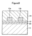
- the buffer layer 12 is in direct contact with the silica substrate 11, as shown in Figure 9, another buffer layer 20 may be interposed between the silica substrate 11 and the buffer layer 12 to reduce the forces arising from the difference in the thermal expansion coefficients of the silica substrate 11 and buffer layer 12.
- the buffer layer 20 has to be of a material with thermal expansion coefficient being between those of the silica substrate 11 and buffer layer 12.
- Preferred materials include silicate glass doped with an amount of germanium (Ge) less than the amount added to the buffer layer 12.
- Example 1 an optical waveguide (directional coupler) was fabricated having the structure shown in Figure 1.
- Germanium (Ge) and boron (B) were added to the buffer layer; the oxide-equivalent amounts were 2.0 mol% and 4.0 mol%, respectively.
- Boron (B) and phosphorus (P) were added to the upper cladding layer; the added amounts were 5.0 mol% and 2.0 mol%, respectively.
- 5.4 mol% of germanium (Ge) was added to the core.
- the refractive index of the buffer layer was 1.44800, that of the upper cladding layer was 1.4483 and that of the core was 1.45409, so the refractive index of the core was approximately 0.4% higher than that of the buffer layer and upper cladding layer.
- the thermal expansion coefficient of the buffer layer and of the upper cladding layer was 12.4 x 10 -7 /°C, meaning that there was effectively 0% difference between the thermal expansion coefficients.
- the thermal expansion coefficient of the core was 11.5 x 10 -7 /°C.
- Example 2 an optical waveguide was fabricated having the same structure as that of Example 1, except that the oxide-equivalent amounts of germanium (Ge) and boron (B) added to the buffer layer were 1.4 mol% and 1.8 mol%, respectively, the amounts of boron (B) and phosphorus (P) added to the upper cladding layer were 1.8 mol% and 1.2 mol%, respectively, and the amount of germanium (Ge) added to the core was 5.2 mol%.
- germanium (Ge) and boron (B) added to the buffer layer were 1.4 mol% and 1.8 mol%, respectively
- the amounts of boron (B) and phosphorus (P) added to the upper cladding layer were 1.8 mol% and 1.2 mol%, respectively
- the amount of germanium (Ge) added to the core was 5.2 mol%.
- the refractive index of the buffer layer was 1.44761, that of the upper cladding layer was 1.44788 and that of the core was 1.45355, so the refractive index of the core was approximately 0.4% higher than that of the buffer layer and upper cladding layer.
- the thermal expansion coefficient of the buffer layer was 8.0 x 10 -7 /°C and that of the upper cladding layer was 8.8 x 10 -7 /°C, meaning that there was a difference of about 10% between the thermal expansion coefficients.
- the thermal expansion coefficient of the core was 11.2 x 10 -7 /°C.
- Example 3 an optical waveguide was fabricated having the same structure as that of Example 1, except that the oxide-equivalent amounts of germanium (Ge) and boron (B) added to the buffer layer were 0.7 mol% and 1.2 mol%, respectively, the amounts of boron (B) and phosphorus (P) added to the upper cladding layer were 1.2 mol% and 1.0 mol%, respectively, and the amount of germanium (Ge) added to the core was 5.0 mol%.
- germanium (Ge) and boron (B) added to the buffer layer were 0.7 mol% and 1.2 mol%, respectively
- the amounts of boron (B) and phosphorus (P) added to the upper cladding layer were 1.2 mol% and 1.0 mol%, respectively
- the amount of germanium (Ge) added to the core was 5.0 mol%.
- the refractive index of the buffer layer was 1.44739, that of the upper cladding layer was 1.44779 and that of the core was 1.45355, so the refractive index of the core was approximately 0.4% higher than that of the buffer layer and upper cladding layer.
- the thermal expansion coefficient of the buffer layer was 7.0 x 10 -7 /°C and that of the upper cladding layer was 7.9 x 10 -7 /°C, meaning that there was a difference of about 13% between the thermal expansion coefficients.
- the thermal expansion coefficient of the core was 11.0 x 10 -7 /°C.
- an optical waveguide was fabricated having the same structure as that of Example 1, except that just germanium (Ge) was added to the buffer layer, the oxide-equivalent amount of the addition being 0.7 mol%, the amounts of boron (B) and phosphorus (P) added to the upper cladding layer were 1.2 mol% and 1.0 mol%, respectively, and the amount of germanium (Ge) added to the core was 5.0 mol%.
- the refractive index of the buffer layer was 1.44775
- that of the upper cladding layer was 1.44778 and that of the core was 1.45355
- the refractive index of the core was approximately 0.4% higher than that of the buffer layer and upper cladding layer.
- the thermal expansion coefficient of the buffer layer was 5.8 x 10 -7 /°C and that of the upper cladding layer was 7 . 9 x 10 -7 /°C, meaning that there was a difference of about 36% between the thermal expansion coefficients.
- the thermal expansion coefficient of the core was 11.0 x 10 -7 /°C.
- an optical waveguide was fabricated having the same structure as that of Example 1, except that just germanium (Ge) was added to the buffer layer, the oxide-equivalent amount of the addition being 1. 0 mol%, the amounts of boron (B) and phosphorus (P) added to the upper cladding layer were 4.5 mol% and 2.0 mol%, respectively, and the amount of germanium (Ge) added to the core was 5.2 mol%.
- the refractive index of the buffer layer was 1.44815
- that of the upper cladding layer was 1.44815 and that of the core was 1.45382
- the refractive index of the core was approximately 0.4% higher than that of the buffer layer and upper cladding layer.
- the thermal expansion coefficient of the buffer layer was 6.2 x 10 -7 /°C and that of the upper cladding layer was 12. 9 x 10 -7 /°C, meaning that there was a difference of about 108% between the thermal expansion coefficients.
- the thermal expansion coefficient of the core was 11.2 x 10 -7 /°C.
- an optical waveguide was fabricated having the same structure as that of Example 1, except that the buffer layer was undoped, the oxide-equivalent amounts of boron (B) and phosphorus (P) added to the upper cladding layer were 4.5 mol% and 1.0 mol%, respectively, and the amount of germanium (Ge) added to the core was 4.8 mol%.
- the refractive index of the buffer layer was 1.4468
- that of the upper cladding layer was 1.4468
- that of the core was 1.45328
- the refractive index of the core was approximately 0.4% higher than that of the buffer layer and upper cladding layer.
- the thermal expansion coefficient of the buffer layer was 6.2 x 10 -7 /°C and that of the upper cladding layer was 11.2 x 10 -7 /°C, meaning that there was a difference of about 81% between the thermal expansion coefficients.
- the thermal expansion coefficient of the core was 10.8 x 10 -7 /°C.
Landscapes
- Physics & Mathematics (AREA)
- Engineering & Computer Science (AREA)
- Microelectronics & Electronic Packaging (AREA)
- General Physics & Mathematics (AREA)
- Optics & Photonics (AREA)
- Optical Integrated Circuits (AREA)
Applications Claiming Priority (2)
| Application Number | Priority Date | Filing Date | Title |
|---|---|---|---|
| JP2004018838 | 2004-01-27 | ||
| JP2004018838A JP3911271B2 (ja) | 2004-01-27 | 2004-01-27 | 光導波路及びその製造方法 |
Publications (1)
| Publication Number | Publication Date |
|---|---|
| EP1560046A1 true EP1560046A1 (de) | 2005-08-03 |
Family
ID=34650772
Family Applications (1)
| Application Number | Title | Priority Date | Filing Date |
|---|---|---|---|
| EP04254602A Withdrawn EP1560046A1 (de) | 2004-01-27 | 2004-07-30 | Lichtwellenleiter und Herstellungsverfahren dafür |
Country Status (4)
| Country | Link |
|---|---|
| US (2) | US7106937B2 (de) |
| EP (1) | EP1560046A1 (de) |
| JP (1) | JP3911271B2 (de) |
| CN (1) | CN100447596C (de) |
Families Citing this family (9)
| Publication number | Priority date | Publication date | Assignee | Title |
|---|---|---|---|---|
| JP3936665B2 (ja) * | 2003-02-17 | 2007-06-27 | Tdk株式会社 | 光導波路 |
| JP2005037464A (ja) * | 2003-07-16 | 2005-02-10 | Matsushita Electric Ind Co Ltd | 光導波路とその製造方法 |
| CN101859001B (zh) * | 2010-06-08 | 2012-06-27 | 浙江大学 | 基于硼锗共掺上包层的二氧化硅光波导器件及制备方法 |
| KR20140027917A (ko) * | 2011-03-25 | 2014-03-07 | 이서영 | 광도파로 및 그 제조방법 |
| CN104409330B (zh) * | 2014-12-02 | 2017-10-20 | 京东方科技集团股份有限公司 | 衬底基板和显示基板及其制作方法、显示装置 |
| JP2019522821A (ja) * | 2016-07-15 | 2019-08-15 | コーニング インコーポレイテッド | 積層構造を有する光導波路物品およびそれを形成する方法 |
| CN107688211B (zh) * | 2016-08-04 | 2020-09-25 | 苏州旭创科技有限公司 | 一种光波导器件及其制作方法 |
| US10998376B2 (en) * | 2019-01-29 | 2021-05-04 | International Business Machines Corporation | Qubit-optical-CMOS integration using structured substrates |
| US12072521B2 (en) * | 2019-10-23 | 2024-08-27 | The Board Of Trustees Of The University Of Illinois | Optical fiber with low thermo-optic coefficient |
Citations (4)
| Publication number | Priority date | Publication date | Assignee | Title |
|---|---|---|---|---|
| JPH10142436A (ja) * | 1996-11-14 | 1998-05-29 | Mitsubishi Cable Ind Ltd | 光導波路構造及びその製造方法 |
| US5904491A (en) * | 1996-04-24 | 1999-05-18 | Northern Telecom Limited | Planar waveguides |
| US20020039474A1 (en) * | 2000-08-23 | 2002-04-04 | Alcatel | Birefringence-free passive optical component |
| US20030152353A1 (en) * | 2002-02-14 | 2003-08-14 | Fujitsu Limited | Planar optical waveguide device |
Family Cites Families (21)
| Publication number | Priority date | Publication date | Assignee | Title |
|---|---|---|---|---|
| JP2585332B2 (ja) * | 1987-12-25 | 1997-02-26 | 株式会社日立製作所 | 導波路型光デバイス |
| JPH0375606A (ja) | 1989-08-17 | 1991-03-29 | Nippon Telegr & Teleph Corp <Ntt> | 埋込み型石英系光導波路およびその製造方法 |
| JP2599488B2 (ja) * | 1990-02-26 | 1997-04-09 | 日本電信電話株式会社 | 光導波回路の特性調整方法およびその方法に使われる光導波回路 |
| JPH07318739A (ja) | 1994-05-20 | 1995-12-08 | Furukawa Electric Co Ltd:The | 石英系光導波路とその製造方法 |
| GB2309096A (en) | 1996-01-09 | 1997-07-16 | Northern Telecom Ltd | Optical waveguide pair with cladding on buffered substrate |
| US5852702A (en) * | 1996-02-28 | 1998-12-22 | Minolta Co., Ltd. | Thin film optical waveguide and optical deflecting device |
| JPH09297237A (ja) | 1996-05-09 | 1997-11-18 | Sumitomo Electric Ind Ltd | 光導波路の製造方法 |
| JP2000329956A (ja) * | 1999-05-24 | 2000-11-30 | Minolta Co Ltd | 光導波路 |
| JP2001194541A (ja) * | 1999-05-31 | 2001-07-19 | Furukawa Electric Co Ltd:The | 光導波回路 |
| US6396988B1 (en) * | 1999-08-13 | 2002-05-28 | Nec Corporation | Optical waveguide device and method of forming the same |
| US6389209B1 (en) * | 1999-09-07 | 2002-05-14 | Agere Systems Optoelectronics Guardian Corp. | Strain free planar optical waveguides |
| GB2366394A (en) * | 2000-08-11 | 2002-03-06 | Kymata Ltd | Integrated optical device with cladding having mesa formation |
| JP4670145B2 (ja) | 2000-12-19 | 2011-04-13 | 住友電気工業株式会社 | 光導波路デバイスの作製方法 |
| US6580862B2 (en) * | 2000-12-22 | 2003-06-17 | Nippon Telegraph And Telephone Corporation | Optical waveguide circuit |
| JP2002250831A (ja) | 2001-02-22 | 2002-09-06 | Hitachi Cable Ltd | 光導波路の製造方法 |
| AUPR368201A0 (en) | 2001-03-13 | 2001-04-12 | Redfern Integrated Optics Pty Ltd | Silica-based optical device fabrication |
| US20030000918A1 (en) | 2001-06-29 | 2003-01-02 | Kheraj Nizar S. | Method for fabricating a protective cap for an optical waveguide core of a planar lightwave circuit device |
| JP2003014959A (ja) | 2001-07-03 | 2003-01-15 | Furukawa Electric Co Ltd:The | 光導波路 |
| US6704487B2 (en) * | 2001-08-10 | 2004-03-09 | Lightwave Microsystems Corporation | Method and system for reducing dn/dt birefringence in a thermo-optic PLC device |
| US6553170B2 (en) * | 2001-08-31 | 2003-04-22 | Lightwave Microsystems Corporation | Method and system for a combination of high boron and low boron BPSG top clad fabrication process for a planar lightwave circuit |
| US6732550B2 (en) * | 2001-09-06 | 2004-05-11 | Lightwave Microsystems, Inc. | Method for performing a deep trench etch for a planar lightwave circuit |
-
2004
- 2004-01-27 JP JP2004018838A patent/JP3911271B2/ja not_active Expired - Fee Related
- 2004-03-26 US US10/810,392 patent/US7106937B2/en not_active Expired - Fee Related
- 2004-07-30 EP EP04254602A patent/EP1560046A1/de not_active Withdrawn
- 2004-09-01 CN CNB2004100749647A patent/CN100447596C/zh not_active Expired - Fee Related
-
2006
- 2006-03-28 US US11/391,792 patent/US20060193584A1/en not_active Abandoned
Patent Citations (4)
| Publication number | Priority date | Publication date | Assignee | Title |
|---|---|---|---|---|
| US5904491A (en) * | 1996-04-24 | 1999-05-18 | Northern Telecom Limited | Planar waveguides |
| JPH10142436A (ja) * | 1996-11-14 | 1998-05-29 | Mitsubishi Cable Ind Ltd | 光導波路構造及びその製造方法 |
| US20020039474A1 (en) * | 2000-08-23 | 2002-04-04 | Alcatel | Birefringence-free passive optical component |
| US20030152353A1 (en) * | 2002-02-14 | 2003-08-14 | Fujitsu Limited | Planar optical waveguide device |
Non-Patent Citations (1)
| Title |
|---|
| PATENT ABSTRACTS OF JAPAN vol. 1998, no. 10 31 August 1998 (1998-08-31) * |
Also Published As
| Publication number | Publication date |
|---|---|
| JP2005215075A (ja) | 2005-08-11 |
| CN1648696A (zh) | 2005-08-03 |
| JP3911271B2 (ja) | 2007-05-09 |
| US7106937B2 (en) | 2006-09-12 |
| CN100447596C (zh) | 2008-12-31 |
| US20060193584A1 (en) | 2006-08-31 |
| US20050163445A1 (en) | 2005-07-28 |
Similar Documents
| Publication | Publication Date | Title |
|---|---|---|
| CN101859001B (zh) | 基于硼锗共掺上包层的二氧化硅光波导器件及制备方法 | |
| US6553170B2 (en) | Method and system for a combination of high boron and low boron BPSG top clad fabrication process for a planar lightwave circuit | |
| EP1219983A2 (de) | Polarisationsunabhängige optische Wellenleiteranordnung | |
| US7372121B2 (en) | GeBPSG top clad for a planar lightwave circuit | |
| CN108415122A (zh) | 一种宽带色散控制波导及控制方法 | |
| US7106937B2 (en) | Optical waveguide and method of fabricating the same | |
| US6690872B2 (en) | Silica based optical waveguide and production method therefor | |
| US6705124B2 (en) | High-density plasma deposition process for fabricating a top clad for planar lightwave circuit devices | |
| US6775454B2 (en) | Silica-based optical waveguide circuit and fabrication method thereof | |
| US6795631B2 (en) | Optical waveguide apparatus and method of producing the same | |
| CN100397119C (zh) | 光波导及其制造方法 | |
| KR100322126B1 (ko) | 광도파로 제작용 기판 및 그 제작방법 | |
| JP3602514B2 (ja) | 石英系光導波回路の作製方法 | |
| US20050213917A1 (en) | Optical waveguide device and method of manufacturing same | |
| CN100414328C (zh) | 用于减小偏振依赖性的平面光学波导及其设备 | |
| JP3530463B2 (ja) | 光導波路 | |
| JP3950588B2 (ja) | 光導波路デバイスの製造方法 | |
| JP2005043497A (ja) | 光導波路 | |
| JP2001074959A (ja) | 埋め込み型光導波路及びその製造方法 | |
| JPH05257021A (ja) | 光導波路の製造方法 | |
| WO2025023287A1 (ja) | 平面光回路、光モジュール、平面光回路の製造方法 | |
| KR100277362B1 (ko) | 더미층을 구비한 광도파로 형성방법 및 그 방법에 의한 광도파로 | |
| KR20020089871A (ko) | 광도파로 소자 및 그의 제조방법 | |
| JP2005062538A (ja) | 光導波路及びその製造方法 | |
| JPH05232335A (ja) | ガラス導波路の製造法 |
Legal Events
| Date | Code | Title | Description |
|---|---|---|---|
| PUAI | Public reference made under article 153(3) epc to a published international application that has entered the european phase |
Free format text: ORIGINAL CODE: 0009012 |
|
| AK | Designated contracting states |
Kind code of ref document: A1 Designated state(s): AT BE BG CH CY CZ DE DK EE ES FI FR GB GR HU IE IT LI LU MC NL PL PT RO SE SI SK TR |
|
| AX | Request for extension of the european patent |
Extension state: AL HR LT LV MK |
|
| 17P | Request for examination filed |
Effective date: 20050902 |
|
| AKX | Designation fees paid |
Designated state(s): AT BE BG CH CY CZ DE DK EE ES FI FR GB GR HU IE IT LI LU MC NL PL PT RO SE SI SK TR |
|
| STAA | Information on the status of an ep patent application or granted ep patent |
Free format text: STATUS: THE APPLICATION IS DEEMED TO BE WITHDRAWN |
|
| 18D | Application deemed to be withdrawn |
Effective date: 20101019 |