EP1552258B1 - Méthode d'encapsulation hermétique d'un dispositif électronique - Google Patents
Méthode d'encapsulation hermétique d'un dispositif électronique Download PDFInfo
- Publication number
- EP1552258B1 EP1552258B1 EP03791044.5A EP03791044A EP1552258B1 EP 1552258 B1 EP1552258 B1 EP 1552258B1 EP 03791044 A EP03791044 A EP 03791044A EP 1552258 B1 EP1552258 B1 EP 1552258B1
- Authority
- EP
- European Patent Office
- Prior art keywords
- housing members
- housing member
- sealing means
- housing
- electronic device
- Prior art date
- Legal status (The legal status is an assumption and is not a legal conclusion. Google has not performed a legal analysis and makes no representation as to the accuracy of the status listed.)
- Expired - Lifetime
Links
Images


Classifications
-
- B—PERFORMING OPERATIONS; TRANSPORTING
- B81—MICROSTRUCTURAL TECHNOLOGY
- B81B—MICROSTRUCTURAL DEVICES OR SYSTEMS, e.g. MICROMECHANICAL DEVICES
- B81B7/00—Microstructural systems ; Auxiliary parts of microstructural devices or systems
- B81B7/0032—Packages or encapsulation
- B81B7/0035—Packages or encapsulation for maintaining a controlled atmosphere inside of the chamber containing the MEMS
- B81B7/0041—Packages or encapsulation for maintaining a controlled atmosphere inside of the chamber containing the MEMS maintaining a controlled atmosphere with techniques not provided for in B81B7/0038
-
- G—PHYSICS
- G01—MEASURING; TESTING
- G01J—MEASUREMENT OF INTENSITY, VELOCITY, SPECTRAL CONTENT, POLARISATION, PHASE OR PULSE CHARACTERISTICS OF INFRARED, VISIBLE OR ULTRAVIOLET LIGHT; COLORIMETRY; RADIATION PYROMETRY
- G01J5/00—Radiation pyrometry, e.g. infrared or optical thermometry
- G01J5/02—Constructional details
- G01J5/04—Casings
-
- G—PHYSICS
- G01—MEASURING; TESTING
- G01J—MEASUREMENT OF INTENSITY, VELOCITY, SPECTRAL CONTENT, POLARISATION, PHASE OR PULSE CHARACTERISTICS OF INFRARED, VISIBLE OR ULTRAVIOLET LIGHT; COLORIMETRY; RADIATION PYROMETRY
- G01J5/00—Radiation pyrometry, e.g. infrared or optical thermometry
- G01J5/02—Constructional details
- G01J5/04—Casings
- G01J5/041—Mountings in enclosures or in a particular environment
- G01J5/045—Sealings; Vacuum enclosures; Encapsulated packages; Wafer bonding structures; Getter arrangements
-
- G—PHYSICS
- G01—MEASURING; TESTING
- G01J—MEASUREMENT OF INTENSITY, VELOCITY, SPECTRAL CONTENT, POLARISATION, PHASE OR PULSE CHARACTERISTICS OF INFRARED, VISIBLE OR ULTRAVIOLET LIGHT; COLORIMETRY; RADIATION PYROMETRY
- G01J5/00—Radiation pyrometry, e.g. infrared or optical thermometry
- G01J5/02—Constructional details
- G01J5/06—Arrangements for eliminating effects of disturbing radiation; Arrangements for compensating changes in sensitivity
- G01J5/068—Arrangements for eliminating effects of disturbing radiation; Arrangements for compensating changes in sensitivity by controlling parameters other than temperature
-
- G—PHYSICS
- G01—MEASURING; TESTING
- G01J—MEASUREMENT OF INTENSITY, VELOCITY, SPECTRAL CONTENT, POLARISATION, PHASE OR PULSE CHARACTERISTICS OF INFRARED, VISIBLE OR ULTRAVIOLET LIGHT; COLORIMETRY; RADIATION PYROMETRY
- G01J5/00—Radiation pyrometry, e.g. infrared or optical thermometry
- G01J5/02—Constructional details
- G01J5/08—Optical arrangements
- G01J5/0806—Focusing or collimating elements, e.g. lenses or concave mirrors
-
- G—PHYSICS
- G02—OPTICS
- G02B—OPTICAL ELEMENTS, SYSTEMS OR APPARATUS
- G02B6/00—Light guides; Structural details of arrangements comprising light guides and other optical elements, e.g. couplings
- G02B6/24—Coupling light guides
- G02B6/42—Coupling light guides with opto-electronic elements
- G02B6/4201—Packages, e.g. shape, construction, internal or external details
- G02B6/4251—Sealed packages
-
- G—PHYSICS
- G02—OPTICS
- G02B—OPTICAL ELEMENTS, SYSTEMS OR APPARATUS
- G02B6/00—Light guides; Structural details of arrangements comprising light guides and other optical elements, e.g. couplings
- G02B6/24—Coupling light guides
- G02B6/42—Coupling light guides with opto-electronic elements
- G02B6/4201—Packages, e.g. shape, construction, internal or external details
-
- G—PHYSICS
- G02—OPTICS
- G02B—OPTICAL ELEMENTS, SYSTEMS OR APPARATUS
- G02B6/00—Light guides; Structural details of arrangements comprising light guides and other optical elements, e.g. couplings
- G02B6/24—Coupling light guides
- G02B6/42—Coupling light guides with opto-electronic elements
- G02B6/4201—Packages, e.g. shape, construction, internal or external details
- G02B6/4204—Packages, e.g. shape, construction, internal or external details the coupling comprising intermediate optical elements, e.g. lenses, holograms
-
- H—ELECTRICITY
- H10—SEMICONDUCTOR DEVICES; ELECTRIC SOLID-STATE DEVICES NOT OTHERWISE PROVIDED FOR
- H10W—GENERIC PACKAGES, INTERCONNECTIONS, CONNECTORS OR OTHER CONSTRUCTIONAL DETAILS OF DEVICES COVERED BY CLASS H10
- H10W76/00—Containers; Fillings or auxiliary members therefor; Seals
- H10W76/60—Seals
-
- H—ELECTRICITY
- H10—SEMICONDUCTOR DEVICES; ELECTRIC SOLID-STATE DEVICES NOT OTHERWISE PROVIDED FOR
- H10W—GENERIC PACKAGES, INTERCONNECTIONS, CONNECTORS OR OTHER CONSTRUCTIONAL DETAILS OF DEVICES COVERED BY CLASS H10
- H10W95/00—Packaging processes not covered by the other groups of this subclass
Definitions
- the present invention relates to hermetic packaging and in particular to an hermetically sealed enclosure and a method for forming said enclosure.
- the invention has particular relevance to hermetically sealed enclosures for electronic devices.
- US-A-4 803 360 describes an infrared radiation detector comprising a pyroelectric detector element sealed in a hermetic housing in a known manner.
- US-A-5 693 942 describes an infrared detector sealed in a hermetic housing containing an inert gas or under reduced pressure.
- Hermetic packaging requires that a sealing step be performed under a controlled atmosphere, usually of an inert gas such as nitrogen or argon. As mentioned above, there may be an additional requirement for the package to be evacuated to a low pressure.
- Outgassing during the sealing processes can introduce contaminants into the controlled atmosphere within the enclosure, which can be of particular concern for high purity hermetic enclosures.
- the sealing process itself can be a significant source of outgassing, which degrades the vacuum level achieved and can introduce a variety of contaminants.
- outgassing is invariably exacerbated if the sealing process includes a heating process.
- US 6,252,229 describes a sealed cavity microstructure having first and second wafers that are positioned relative to each other so as to from a cavity there-between.
- the microstructure includes a pressure seal and a structural bond arranged between the first and second wafers to integrate said wafers.
- JP 11 274341 describes a vacuum sealing method of encapsulating a piezoelectric part in which a metal cap is mechanically press-fitted to an outer-peripheral part of a ceramic substrate to form an airtight seal via a contraction / caulking plastic joint.
- a method of hermetically packaging an electronic device, in an enclosure comprising mutually inter-engageable first and second housing members adapted to inter-engage to form an interference fit there between comprises the steps of
- the method provides a simple and cost effective sealing procedure for hermetically packaging the electronic device. Furthermore, the sealing step reduces contamination of the controlled atmosphere and reduces outgassing. Where the controlled atmosphere comprises a vacuum, degradation of the vacuum during sealing is reduced.
- the first housing member comprises a base portion, to which the electronic device is secured during the securing step, and an engagement portion adapted to engage with the second housing member, and wherein the method further comprises the step of attaching the base portion to the engagement portion prior to engaging the first and second housing members.
- the step of attaching the base portion of the first housing member to the engagement portion does not need to be performed in an inert atmosphere or a vacuum, as it would be in a conventional vacuum assembly process. Accordingly, a wider range of processes can be used to package the electronic device and hence the assembly cost can be reduced.
- the sealing means may comprise at least one of a metal, a eutectic alloy, an elastomer and an adhesive,
- the sealing means comprise an indium seal or a compressible elastomeric ring.
- the method further comprises the intermediate step of applying the sealing means to least one of the first and second housing members prior to engaging the first and second housing members.
- the enclosure comprises retaining means disposed adjacent the sealing means so as to retain the sealing means.
- the second housing member comprises a first substantially transmissive optical element and an engagement portion adapted to engage with the first housing member.
- the hermetic seal may be provided between the first housing member and the first optical element via said sealing means.
- the second housing member is adapted to receive a second substantially transmissive optical element.
- the controlled atmosphere comprises an inert gas.
- the inert gas may comprise at least one of nitrogen and argon.
- the controlled atmosphere comprises a vacuum.
- the step of engaging the first and second housing members may include the step of bonding said housing members.
- the bonding step may comprise one of friction welding and friction soldering.
- the first and second housing members comprise metal cylinders having a substantially circular cross section.
- an electronic device comprising an electronic element, a first housing member, and a second housing member, the first and second housing members having an engagement hermetic seal there between so as to define around the electronic element an hermetic enclosure having a controlled atmosphere within.
- an electronic device comprising an electronic element, a first housing member, and a second housing member, the first and second housing members defining an hermetic enclosure, wherein the electronic element is located within the hermetic enclosure and wherein the hermetic enclosure is formed by engaging the first and second housing members in a controlled atmosphere such that an engagement hermetic seal is provided there between.
- the above electronic devices are advantageous in that they utilise a simple and cost effective hermetic seal. Furthermore, the hermetic seal reduces contamination of the controlled atmosphere and reduces outgassing during the sealing process. Where the controlled atmosphere comprises a vacuum, degradation of the vacuum during sealing is reduced.
- the engagement hermetic seal comprises an interference seal between the first and second housing members.
- the engagement hermetic seal comprises a friction weld between the first and second housing members.
- the electronic device according to the second or third aspect of the present invention further comprises sealing means interposed between the first and second housing members, said sealing means providing the engagement hermetic seal.
- the first and second housing members may be held in engagement by an interference fit there between.
- the sealing means comprise at least one of a metal, a eutectic alloy, an elastomer and an adhesive.
- the sealing means comprise an indium seal or a compressible elastomeric ring.
- the enclosure further comprises spacer means disposed adjacent the sealing means so as to preclude over-compression of the sealing means.
- the enclosure may comprise retaining means disposed adjacent the sealing means so as to retain the sealing means.
- the second housing member comprises a first substantially transmissive optical element and an engagement portion adapted to engage with the first housing member.
- the first optical element may comprise a lens.
- the first optical element comprises at least one of chalcogenide glass, silicon and germanium.
- the engagement hermetic seal may be provided between the first housing member and the first optical element via the sealing means.
- the second housing member includes a second substantially transmissive optical element.
- the second optical element may comprises chalcogenide glass.
- the controlled atmosphere comprises an inert gas.
- the inert gas may comprise at least one of nitrogen and argon.
- the controlled atmosphere comprises a vacuum.
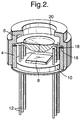
- an hermetically sealed enclosure (2) comprises a first housing member (4) and a second housing member (6) which together enclose an electronic device (8) disposed within said housing members.
- the housing members (4, 6) are arranged such that they fit together to form an hermetic seal around the electronic device.
- the housing members (4, 6) may comprise inter-engageable cylinders.
- the second housing member (6) has a closed end to provide a lid for the hermetic enclosure.
- Figure 1 shows the first housing member (4) attached to a separate base (10). However, a separate base is not required if the first housing member (4) is closed cylinder, in which case the base (10) is integral to the first housing member (4).
- the cylinders may be fabricated from metal, ceramic, glass, plastic or any other suitable material. In particular, the cylinders may exhibit a substantially circular cross section.
- the electronic device (8) is disposed on a base (10) and connected to external connections (12) via feedthroughs (14) on the base (10).
- the feedthroughs (14) may comprise conventional glass-to-metal feedthroughs.
- the first and second housing members (4, 6) may be arranged such that they fit together to form an interference fit, thereby providing an hermetic seal around the electronic device.
- a seal (16) may be disposed between the first housing member (4) and the second housing member (6). The seal (16) provides a continuous, airtight connection between the two housing members (4, 6).
- the seal (16) may be a ring of soft metal such as indium located on the top surface of the first housing member (4).
- the seal (16) may be accompanied by one or more additional ring (18) which acts as a spacer layer to prevent over-compression of the seal. Additionally, or alternatively, the ring (18) may act as a dam to prevent the escape of the sealing material (16).
- the additional ring (18) which acts as the spacer and/or dam features can also be designed into the shape of the housing member (4, 6), thus reducing the number of components and assembly steps. Location features may also be included to ease assembly.
- sealing materials can be used, for example other soft metals, solders and eutectic alloys, as well as rubber seals and glues.
- an adhesive could be applied outside of the seal (16) to add mechanical strength to the seal (16).
- the seal material could be added in vacuum, for example by vacuum evaporation.
- the sealing ring (16) could also be deposited onto the assembly by an overmoulding process in the case of an elastomeric seal.
- the hermetic enclosure is fabricated as follows.
- the electronic device (8) is attached to the base (10) (for example, a transistor can header such as a TO-5 or a TO-8 header) by industry standard processes. Any conventional low-outgassing die attach methods may be used. If required, the electrical connections are then bonded to the feedthroughs (14) (for example, glass-to-metal feedthroughs) on the base (10), also in a standard manner.
- the first housing member (4) comprising a metal cylinder in this instance, is attached to the base (10).
- the metal cylinder may be formed by drawing, punching or machining processes. Additional features, such as alignment features or a lip to provide a reduced aperture may be used on this part in order to assemble the part with a second housing member (6) of the required geometry.
- the metal cylinder (4) may be attached by welding, soldering, gluing, crimping or other attachment processes, which can be selected for their cost and hermeticity properties.
- welding resistance welding, electron-beam welding, laser welding, or other welding processes can be used as appropriate for the size and geometry of the package.
- this process is not performed in an inert atmosphere or a vacuum, as it would be in a conventional metal can vacuum assembly process, means that a wider range of processes can be used and the assembly cost can be reduced. Whilst the above step does not require an inert atmosphere or a vacuum, it may be desirable to fabricate the hermetic enclosure and attach the electronic device under clean-room conditions to avoid particulate contamination of the device. This sub-assembly, along with the other package components, can then be stored in under controlled conditions, at an elevated temperature until required. This reduces the need for time-consuming bake-out processes at the time of assembly.
- the next assembly step is performed under a controlled atmosphere.
- the controlled atmosphere may comprise an inert gas, for example nitrogen or argon. Additionally, or alternatively, the controlled atmosphere may comprise a vacuum.
- the term vacuum shall refer to a decrease of pressure below normal ambient atmospheric pressure. Note that the controlled atmosphere under which this next assembly step is performed is not merely a clean-room environment as used above for fabricating the hermetic enclosure.
- the second housing member (6) is pressed down onto the seal (16), in this case an indium sealing ring. Location features allow this assembly process to be performed with high accuracy and at low cost.
- the second housing member (6) may be designed to slide over the first housing member (4), or vice versa, and to form an interference fit therewith. In this case, no additional means are required to hold the enclosure together.
- the interference fit itself may be used to provide a seal in this case.
- the housing members (4, 6) comprise metal cylinders
- the second housing member (6) may be heated prior to assembly and allowed to cool and contract over the first housing member (4), thus improving the seal.
- the housing members (4, 6) comprise metal cylinders
- the friction due to the second housing member (6) being moved over the first housing member (4) can be used to produce heating and produce a friction welded seal or to melt a pre-placed mass of solder, referred to herein as frictional soldering.
- the seal (16) consists of indium solder, although, as mentioned above, other sealing methods can be used.
- the above method of forming the hermetic enclosure is advantageous in that only an alignment and compression operation must be performed under a controlled atmosphere, thus simplifying the manufacture.
- the low part count and simple assembly procedure enables a very low cost hermetic enclosure to be manufactured.
- the fabrication process uses a low temperature sealing step, which has several advantages. Firstly, there is no outgassing during the sealing step. Secondly, materials of differing thermal expansion coefficients can be joined. Thirdly, materials subject to damage by heating or thermal shock can be joined.
- getters may be included in the package to remove gases which accumulate due to leakage or outgassing over a period of several years, thereby maintaining a high level of vacuum over a long period of time.
- the internal volume of the hermetically sealed enclosure (2) is arranged to be as large as possible for a given application so as to mitigate the effects of leakage and outgassing on the vacuum level within the enclosure.
- a useable vacuum level can be sustained over a long period of time by maximising the internal volume of the hermetically sealed enclosure (2) as suggested above.
- the enclosure may be arranged to exhibit an initial internal pressure of 1 Pascal, degrading to a pressure of 10 - 100 Pascal over the design life of the device (referred to below as the end-of-life pressure).
- the initial and end-of-life pressures within enclosure may be specified as design parameters at the outset, in which case the internal volume of the enclosure can be calculated and optimised such that the pressure within the enclosure at the end of the design life does not exceed the design specification.
- the calculation requires an appreciation of the outgassing and leakage mechanisms at work within the enclosure, both of which would be familiar to the skilled person.
- the end-of-life pressure shall not exceed 100 Pascal, 80 Pascal, 60 Pascal, 40 Pascal, 20 Pascal, or 10 Pascal depending on the particular application.
- the hermetically sealed package will have an internal volume greater than 0.5 cm 3 (cubic centimetres), 0.75cm 3 or 1cm 3 .
- the maximum internal volume of the hermetically sealed package will be less than 2 cm 3 , 1.75cm 3 , 1.5cm 3 or 1.25cm 3 .
- the design life of the device is anticipated to be in excess of 10 years.
- the second housing member (6) may perform additional functions, such as providing an aperture for electromagnetic radiation to enter or leave.
- the second housing member (6) may hold one or more additional optical components in place.
- the second housing member (6) comprises an optical element (20) providing a window or lens to transmit electromagnetic radiation in a preferred frequency range.
- the optical element (20) may take the form of an infra-red window or lens made from a chalcogenide glass material such as the one of the AMTIR materials manufactured by Amorphous Materials or one of the GASIR materials manufactured by Umicore. These lenses have the advantage of low manufacturing cost.
- the optical element (20) may take the form of an infra-red window or lens made from silicon or germanium.
- a lens integral to the second housing member (6) enables electromagnetic radiation to be focussed onto the electronic device (8) housed within the hermetically sealed enclosure (2), and obviates external optical components.
- the electronic device (8) may comprise an optical detector, for example an optical detector sensitive to electromagnetic radiation having wavelengths in the visible spectrum, or a microbolometer detector sensitive to electromagnetic radiation having wavelengths in the infrared spectrum (for example thermal radiation).
- the electronic device may comprise a multi-element detector, in which case the integral lens enables a complete imaging system to be achieved within the hermetically sealed enclosure (2).
- the lens may comprise a simple lens having a single element, a compound lens having a plurality of elements, a fresnel lens, or an array of lenses, for example an array of microlenses.
- the optical element (20) may be metallised at the edges to enable a wider range of vacuum sealing processes, for example soldering processes.
- a soldering process may be used to attach the optical element (20) to the second housing member (6) prior to assembling the first and second housing members (4, 6) as described above.
- a low temperature soldering process may be incorporated into the sealing steps performed in a controlled atmosphere. The soldering process creates negligible outgassing and so may be used without compromising the purity of the controlled atmosphere within the hermetic enclosure (2) or the level of the vacuum therein.
- FIG 3 shows an exploded schematic representation of an hermetic enclosure according to the present invention. Elements in common with figures 1 and 2 are given like reference numerals.
- Figure 4 shows an alternative embodiment of the present invention in which the optical element (20) is used in combination with an additional optical element (22).
- the first optical element (20) comprises an infrared lens or window made from silicon or germanium.
- a silicon or germanium window has improved mechanical and thermo-mechanical properties compared to the chalcogenide glass lens.
- the additional optical element (22) may comprise a chalcogenide glass lens glued in an accurately-defined location above the first optical element (20), the location being defined by location feature(s) in the second housing member (6).
- the relatively fragile lens (22) is not directly exposed to the vacuum or to other mechanical and thermal stresses which may be involved in the vacuum sealing process.
- the first optical element (20) may be metallised at the edges to enable a wider range of vacuum sealing processes, for example soldering processes.
- the components are largely made of metal, the components may alternatively or additionally be made of ceramic (for example, using a ceramic chip carrier in place of the metal transistor can header), glass, plastic or other suitable materials.
- the hermetically sealed enclosure of the present invention may be used to house thermal detectors, for example microbolometer arrays.
Landscapes
- Physics & Mathematics (AREA)
- General Physics & Mathematics (AREA)
- Spectroscopy & Molecular Physics (AREA)
- Engineering & Computer Science (AREA)
- Microelectronics & Electronic Packaging (AREA)
- Computer Hardware Design (AREA)
- Optics & Photonics (AREA)
- Photometry And Measurement Of Optical Pulse Characteristics (AREA)
- Radiation Pyrometers (AREA)
- Packaging Frangible Articles (AREA)
- Packages (AREA)
Claims (15)
- Un procédé pour emballer hermétiquement un dispositif électronique (8), dans une enceinte (2) comprenant des premier et deuxième éléments formant boîtier (4, 6) mutuellement inter-engageables, adaptés à s'inter-engager en formant un ajustement étroit entre eux, comprenant les étapes consistant à :(i) fixer le dispositif électronique (8) au premier élément formant boîtier (4),(ii) mettre en engagement les premier et deuxième éléments formant boîtier (4, 6) sous une atmosphère contrôlée de telle sorte que les premier et deuxième éléments formant boîtier (4, 6) sont maintenus en engagement selon un ajustement étroit entre eux et que, de ce fait, une jonction étanche soit réalisée entre eux,
caractérisé par les étapes intermédiaires consistant à :(iii) interposer des moyens d'étanchéité (16) entre lesdits premier et deuxième éléments formant boîtier (4, 6), et(iv) disposer des moyens formant entretoise (18) de façon adjacente auxdits moyens d'étanchéité (16) de manière à empêcher une compression excessive des moyens d'étanchéité (16) pendant l'étape de mise en engagement,
et les moyens d'étanchéité (16) fournissant une connexion étanche à l'air entre les premier et deuxième éléments formant boîtier (4, 6). - Un procédé selon la revendication 1, dans lequel le premier élément formant boîtier (4) comprend une partie de base (10), à laquelle le dispositif électronique (8) est fixé au cours de l'étape de fixation, et une partie d'engagement adaptée pour venir en engagement avec le deuxième élément formant boîtier (6), et dans lequel le procédé comprend en outre l'étape consistant à fixer la partie de base (10) à la partie d'engagement avant de mettre en engagement les premier et deuxième éléments formant boîtier (4, 6).
- Un procédé selon la revendication 1 ou la revendication 2, dans lequel les moyens d'étanchéité (16) comprennent au moins un parmi : un métal, un alliage eutectique, un élastomère et un adhésif.
- Un procédé selon l'une quelconque des revendications 1 à 3, dans lequel les moyens d'étanchéité (16) comprennent un joint en indium.
- Un procédé selon l'une quelconque des revendications 1 à 3, dans lequel les moyens d'étanchéité (16) comprennent un anneau en élastomère compressible.
- Un procédé selon l'une quelconque des revendications précédentes et comprenant en outre l'étape intermédiaire consistant à appliquer les moyens d'étanchéité (16) à au moins l'un des premier et deuxième éléments formant boîtier (4, 6) avant d'amener en engagement les premier et deuxième éléments formant boîtier (4, 6).
- Un procédé selon l'une quelconque des revendications précédentes, dans lequel le deuxième élément formant boîtier (6) comprend un premier élément optique (20) sensiblement transmissif et une partie d'engagement adaptée pour venir en engagement avec le premier élément formant boîtier (4).
- Un procédé selon la revendication 7, dans lequel la jonction étanche est aménagée entre le premier élément formant boîtier (4) et le premier élément optique (20).
- Un procédé selon la revendication 7 ou la revendication 8, dans lequel le deuxième élément formant boîtier (6) est adapté pour recevoir un deuxième élément optique (22) sensiblement transmissive.
- Un procédé selon l'une quelconque des revendications précédentes, dans lequel l'atmosphère contrôlée comprend un gaz inerte.
- Un procédé selon la revendication 10, dans lequel le gaz inerte comprend au moins un parmi l'azote et l'argon.
- Un procédé selon l'une quelconque des revendications précédentes, dans lequel l'atmosphère contrôlée comprend un vide.
- Un procédé selon l'une quelconque des revendications précédentes, dans lequel l'étape consistant à mettre en engagement les premier et deuxième éléments formant boîtier (4, 6) comprend l'étape consistant à relier lesdits éléments formant boîtier.
- Un procédé selon la revendication 13, dans lequel l'étape de liaison comprend l'un parmi : le soudage par friction et le brasage par friction.
- Un procédé selon l'une quelconque des revendications précédentes, dans lequel les premier et deuxième éléments formant boîtier (4, 6) comprennent des cylindres métalliques ayant une section transversale sensiblement circulaire.
Applications Claiming Priority (3)
| Application Number | Priority Date | Filing Date | Title |
|---|---|---|---|
| GB0220274A GB2392555A (en) | 2002-09-02 | 2002-09-02 | Hermetic packaging |
| GB0220274 | 2002-09-02 | ||
| PCT/GB2003/003737 WO2004020961A1 (fr) | 2002-09-02 | 2003-09-01 | Encapsulation hermetique |
Publications (2)
| Publication Number | Publication Date |
|---|---|
| EP1552258A1 EP1552258A1 (fr) | 2005-07-13 |
| EP1552258B1 true EP1552258B1 (fr) | 2016-03-09 |
Family
ID=9943288
Family Applications (1)
| Application Number | Title | Priority Date | Filing Date |
|---|---|---|---|
| EP03791044.5A Expired - Lifetime EP1552258B1 (fr) | 2002-09-02 | 2003-09-01 | Méthode d'encapsulation hermétique d'un dispositif électronique |
Country Status (6)
| Country | Link |
|---|---|
| US (1) | US7348203B2 (fr) |
| EP (1) | EP1552258B1 (fr) |
| JP (1) | JP4664675B2 (fr) |
| AU (1) | AU2003260750A1 (fr) |
| GB (1) | GB2392555A (fr) |
| WO (1) | WO2004020961A1 (fr) |
Families Citing this family (48)
| Publication number | Priority date | Publication date | Assignee | Title |
|---|---|---|---|---|
| US6856007B2 (en) | 2001-08-28 | 2005-02-15 | Tessera, Inc. | High-frequency chip packages |
| US6972480B2 (en) | 2003-06-16 | 2005-12-06 | Shellcase Ltd. | Methods and apparatus for packaging integrated circuit devices |
| JP2007528120A (ja) | 2003-07-03 | 2007-10-04 | テッセラ テクノロジーズ ハンガリー コルラートルト フェレロェセーギュー タールシャシャーグ | 集積回路装置をパッケージングする方法及び装置 |
| WO2005031862A1 (fr) | 2003-09-26 | 2005-04-07 | Tessera, Inc. | Structure et procede pour l'elaboration de puces coiffees hermetiques |
| DE102004020858A1 (de) * | 2004-04-28 | 2005-11-24 | Siemens Ag | Sensoranordnung und Verfahren zum Herstellen einer Sensoranordnung |
| DE102004028022B4 (de) | 2004-06-09 | 2006-11-16 | Perkinelmer Optoelectronics Gmbh & Co.Kg | Sensor |
| US20060023107A1 (en) * | 2004-08-02 | 2006-02-02 | Bolken Todd O | Microelectronic imagers with optics supports having threadless interfaces and methods for manufacturing such microelectronic imagers |
| US7429494B2 (en) * | 2004-08-24 | 2008-09-30 | Micron Technology, Inc. | Microelectronic imagers with optical devices having integral reference features and methods for manufacturing such microelectronic imagers |
| GB0424934D0 (en) | 2004-11-12 | 2004-12-15 | Qinetiq Ltd | Infrared detector |
| JP4453546B2 (ja) * | 2004-12-22 | 2010-04-21 | 日産自動車株式会社 | パッケージ素子 |
| US8143095B2 (en) | 2005-03-22 | 2012-03-27 | Tessera, Inc. | Sequential fabrication of vertical conductive interconnects in capped chips |
| US7449779B2 (en) | 2005-03-22 | 2008-11-11 | Tessera, Inc. | Wire bonded wafer level cavity package |
| DE102005038864A1 (de) * | 2005-08-17 | 2007-03-01 | Stryker Leibinger Gmbh & Co. Kg | Chirurgische Elektrowerkzeug und Betätigungseinheit hierfür |
| US7936062B2 (en) | 2006-01-23 | 2011-05-03 | Tessera Technologies Ireland Limited | Wafer level chip packaging |
| KR101076666B1 (ko) * | 2006-05-25 | 2011-10-26 | 파나소닉 전공 주식회사 | 적외선 센서 |
| US7677765B2 (en) * | 2006-06-15 | 2010-03-16 | Avago Technologies General Ip (Singapore) Pte. Ltd. | Light emitting device having a metal can package for improved heat dissipation |
| US8604605B2 (en) | 2007-01-05 | 2013-12-10 | Invensas Corp. | Microelectronic assembly with multi-layer support structure |
| TW200841541A (en) * | 2007-04-04 | 2008-10-16 | Amtran Technology Co Ltd | Package structure of optical-element |
| US7968986B2 (en) * | 2007-05-07 | 2011-06-28 | Innovative Micro Technology | Lid structure for microdevice and method of manufacture |
| FR2923009B1 (fr) * | 2007-10-30 | 2011-11-04 | Ulis | Detecteur de rayonnement electromagnetique et notamment detecteur infrarouge. |
| US20100116970A1 (en) * | 2008-11-12 | 2010-05-13 | Wen-Long Chou | Photo detection device |
| US8092044B1 (en) | 2008-11-21 | 2012-01-10 | Tomar Electronics, Inc. | LED light assembly and related methods |
| DE102009004724A1 (de) * | 2009-01-15 | 2010-07-22 | Osram Opto Semiconductors Gmbh | Verfahren zur Herstellung eines optoelektronischen Bauteils und optoelektronisches Bauteil |
| JP5327042B2 (ja) * | 2009-03-26 | 2013-10-30 | 豊田合成株式会社 | Ledランプの製造方法 |
| JP2011112508A (ja) * | 2009-11-26 | 2011-06-09 | Nippon Ceramic Co Ltd | 焦電型赤外線検出装置 |
| KR101631958B1 (ko) * | 2010-01-14 | 2016-06-20 | 엘지전자 주식회사 | 입력 장치 및 이를 구비하는 이동 단말기 |
| JP5467896B2 (ja) * | 2010-03-05 | 2014-04-09 | 株式会社タムロン | 赤外線ズームレンズ |
| JP2011186070A (ja) * | 2010-03-05 | 2011-09-22 | Tamron Co Ltd | 赤外線ズームレンズ |
| KR101144665B1 (ko) * | 2010-09-20 | 2012-05-24 | 옵티시스 주식회사 | 파장 분할 다중화 및 역다중화 장치 |
| JP5287906B2 (ja) * | 2011-03-02 | 2013-09-11 | オムロン株式会社 | 赤外線温度センサ、電子機器、および赤外線温度センサの製造方法 |
| US10078007B2 (en) | 2011-12-14 | 2018-09-18 | Panasonic Intellectual Property Management Co., Ltd. | Infrared sensor |
| CN103988062B (zh) | 2011-12-14 | 2017-09-22 | 松下知识产权经营株式会社 | 红外传感器 |
| US8731347B2 (en) * | 2012-10-11 | 2014-05-20 | Avago Technologies General Ip (Singapore) Pte. Ltd. | Lens standoff and protection for optical communication systems |
| US20140238726A1 (en) * | 2013-02-28 | 2014-08-28 | Cooper Technologies Company | External moisture barrier package for circuit board electrical component |
| US10884551B2 (en) | 2013-05-16 | 2021-01-05 | Analog Devices, Inc. | Integrated gesture sensor module |
| US9590129B2 (en) | 2014-11-19 | 2017-03-07 | Analog Devices Global | Optical sensor module |
| CN105761439B (zh) * | 2014-12-17 | 2019-09-13 | 富泰华工业(深圳)有限公司 | 侦测空气污染的移动终端、系统及方法 |
| US9869464B2 (en) | 2015-09-23 | 2018-01-16 | Cooper Technologies Company | Hermetically-sealed light fixture for hazardous environments |
| US9684141B1 (en) * | 2016-04-25 | 2017-06-20 | Applied Optoelectronics, Inc. | Techniques for reducing ingress of foreign matter into an optical subassembly |
| US10712197B2 (en) | 2018-01-11 | 2020-07-14 | Analog Devices Global Unlimited Company | Optical sensor package |
| JP2020016519A (ja) * | 2018-07-25 | 2020-01-30 | 日本電気硝子株式会社 | 光学部品 |
| US11293551B2 (en) * | 2018-09-30 | 2022-04-05 | ColdQuanta, Inc. | Break-seal system with breakable-membrane bridging rings |
| US10996409B2 (en) * | 2018-10-22 | 2021-05-04 | Ii-Vi Delaware, Inc. | Plastic composite lens array in optical networks |
| CN111256831B (zh) * | 2018-11-30 | 2021-10-12 | 宁波方太厨具有限公司 | 一种红外温度传感器 |
| CN110082870B (zh) * | 2019-05-31 | 2024-06-25 | 浙江舜宇光学有限公司 | To-can管帽 |
| JP7738224B2 (ja) * | 2021-03-04 | 2025-09-12 | パナソニックIpマネジメント株式会社 | 赤外線検出装置 |
| JP2022179073A (ja) * | 2021-05-21 | 2022-12-02 | 株式会社エンプラス | 光レセプタクルおよび光モジュール |
| US20240006267A1 (en) * | 2022-06-29 | 2024-01-04 | Texas Instruments Incorporated | Hermetic Package Cooling Using Silver Tubes with Getter Absorption Material |
Citations (4)
| Publication number | Priority date | Publication date | Assignee | Title |
|---|---|---|---|---|
| US4803360A (en) * | 1984-09-19 | 1989-02-07 | U.S. Philips Corp. | Infrared radiation detector with flanged semiconductor window |
| US5693942A (en) * | 1995-04-07 | 1997-12-02 | Ishizuka Electronics Corporation | Infrared detector |
| JPH10242317A (ja) * | 1997-02-25 | 1998-09-11 | Nec Kansai Ltd | 気密パッケージ及びこの気密パッケージを利用した電子部品 |
| JPH11274341A (ja) * | 1998-03-20 | 1999-10-08 | Wti Kk | チップタイプ圧電部品 |
Family Cites Families (24)
| Publication number | Priority date | Publication date | Assignee | Title |
|---|---|---|---|---|
| US3880528A (en) * | 1973-07-02 | 1975-04-29 | Tektronix Inc | Light probe |
| US4307934A (en) * | 1978-05-08 | 1981-12-29 | General Dynamics, Pomona Division | Packaged fiber optic modules |
| US4477828A (en) * | 1982-10-12 | 1984-10-16 | Scherer Jeremy D | Microcircuit package and sealing method |
| GB2165639B (en) * | 1984-08-24 | 1988-01-27 | Philips Electronic Associated | Pyroelectric infra-red detector |
| JPH02105133U (fr) * | 1989-02-08 | 1990-08-21 | ||
| JP2684219B2 (ja) * | 1989-07-05 | 1997-12-03 | 三菱電機株式会社 | 光半導体モジュール |
| SE465001B (sv) | 1989-11-14 | 1991-07-08 | Asea Brown Boveri | Laserdiod med inbyggd signaldetektor |
| US5119462A (en) * | 1990-01-29 | 1992-06-02 | 501 Nippon Sheet Glass Co., Ltd. | Photosemiconductor and optical fiber welded module |
| US5198664A (en) * | 1991-07-18 | 1993-03-30 | Banner Engineering Corporation | Photoelectric sensor assembly having compressible and sealing members |
| JPH05283546A (ja) * | 1992-03-30 | 1993-10-29 | Nippon Dempa Kogyo Co Ltd | 抵抗溶接方法 |
| JP2954788B2 (ja) * | 1992-07-06 | 1999-09-27 | アルプス電気株式会社 | 光電変換接続装置およびその製造方法 |
| BE1007779A3 (nl) * | 1993-11-25 | 1995-10-17 | Philips Electronics Nv | Opto-electronische halfgeleiderinrichting met een straling-emitterende halfgeleiderdiode en werkwijze van een dergelijke inrichting. |
| US5804827A (en) * | 1995-10-27 | 1998-09-08 | Nikon Corporation | Infrared ray detection device and solid-state imaging apparatus |
| US5914488A (en) * | 1996-03-05 | 1999-06-22 | Mitsubishi Denki Kabushiki Kaisha | Infrared detector |
| JPH09297064A (ja) * | 1996-05-07 | 1997-11-18 | Matsushita Electric Ind Co Ltd | 焦電型赤外線センサ |
| US6092935A (en) * | 1997-08-22 | 2000-07-25 | Siemens Aktiengesellschaft | Optoelectronic transmitting and/or receiving module and method for its production |
| EP0951068A1 (fr) * | 1998-04-17 | 1999-10-20 | Interuniversitair Micro-Elektronica Centrum Vzw | Procédé de fabrication pour une microstructure avec une cavité interne |
| US6252229B1 (en) * | 1998-07-10 | 2001-06-26 | Boeing North American, Inc. | Sealed-cavity microstructure and microbolometer and associated fabrication methods |
| JP2000059173A (ja) * | 1998-08-07 | 2000-02-25 | Seiko Epson Corp | 圧電振動子、圧電振動素子封止用容器および圧電振動素子封止方法 |
| JP2000208051A (ja) * | 1999-01-19 | 2000-07-28 | Canon Inc | 封止方法及び密封容器と画像表示装置及び真空排気装置 |
| AU1249601A (en) | 1999-08-31 | 2001-03-26 | Epitaxx, Inc. | Integrated wavelength selective photodiode module |
| US6686588B1 (en) * | 2001-01-16 | 2004-02-03 | Amkor Technology, Inc. | Optical module with lens integral holder |
| US6758611B1 (en) * | 2001-03-12 | 2004-07-06 | Bradley S. Levin | Radially symmetrical optoelectric module |
| US6890834B2 (en) * | 2001-06-11 | 2005-05-10 | Matsushita Electric Industrial Co., Ltd. | Electronic device and method for manufacturing the same |
-
2002
- 2002-09-02 GB GB0220274A patent/GB2392555A/en not_active Withdrawn
-
2003
- 2003-09-01 US US10/523,528 patent/US7348203B2/en not_active Expired - Lifetime
- 2003-09-01 WO PCT/GB2003/003737 patent/WO2004020961A1/fr not_active Ceased
- 2003-09-01 AU AU2003260750A patent/AU2003260750A1/en not_active Abandoned
- 2003-09-01 EP EP03791044.5A patent/EP1552258B1/fr not_active Expired - Lifetime
- 2003-09-01 JP JP2004532307A patent/JP4664675B2/ja not_active Expired - Fee Related
Patent Citations (4)
| Publication number | Priority date | Publication date | Assignee | Title |
|---|---|---|---|---|
| US4803360A (en) * | 1984-09-19 | 1989-02-07 | U.S. Philips Corp. | Infrared radiation detector with flanged semiconductor window |
| US5693942A (en) * | 1995-04-07 | 1997-12-02 | Ishizuka Electronics Corporation | Infrared detector |
| JPH10242317A (ja) * | 1997-02-25 | 1998-09-11 | Nec Kansai Ltd | 気密パッケージ及びこの気密パッケージを利用した電子部品 |
| JPH11274341A (ja) * | 1998-03-20 | 1999-10-08 | Wti Kk | チップタイプ圧電部品 |
Also Published As
| Publication number | Publication date |
|---|---|
| EP1552258A1 (fr) | 2005-07-13 |
| AU2003260750A1 (en) | 2004-03-19 |
| US7348203B2 (en) | 2008-03-25 |
| JP4664675B2 (ja) | 2011-04-06 |
| WO2004020961A1 (fr) | 2004-03-11 |
| GB2392555A (en) | 2004-03-03 |
| GB0220274D0 (en) | 2002-10-09 |
| US20060166407A1 (en) | 2006-07-27 |
| JP2005537473A (ja) | 2005-12-08 |
Similar Documents
| Publication | Publication Date | Title |
|---|---|---|
| US7348203B2 (en) | Hermetic packaging | |
| US7164199B2 (en) | Device packages with low stress assembly process | |
| US11529701B2 (en) | Method and apparatus for producing a hermetic vacuum joint at low temperature | |
| JP2005537473A5 (fr) | ||
| EP1741668A2 (fr) | Procédé pour encapsuler un dispositif MEMS et dispositif encapsulé | |
| EP1295335B1 (fr) | Boitier de microdispositif miniature et son procede de fabrication | |
| EP1540727B1 (fr) | Procede de fermeture d'une microcavite et boitier comprenant au moins une microcavite | |
| US20020043706A1 (en) | Miniature Microdevice Package and Process for Making Thereof | |
| US7736946B2 (en) | System and method for sealing a MEMS device | |
| US7442576B2 (en) | Placement of absorbing material in a semiconductor device | |
| CN1740758B (zh) | 探测电磁辐射部件,含其的红外光学成像单元及实现过程 | |
| US5986208A (en) | Waveguide window assembly and microwave electronics package | |
| JP2020059119A (ja) | 二重のシールリングを含むウエハレベルmemsパッケージ | |
| JP2003254820A (ja) | 赤外線検出器 | |
| US20220283034A1 (en) | Method for Producing a Thermal Infrared Sensor Array in a Vacuum-Filled Wafer-Level Housing | |
| US7772041B2 (en) | Method of sealing or welding two elements to one another | |
| US4349831A (en) | Semiconductor device having glass and metal package | |
| US7524704B2 (en) | Method for encapsulating a component, especially an electric or electronic component, by means of an improved solder seam | |
| JP2008298205A (ja) | 真空封止装置 | |
| US4766316A (en) | Disc detector assembly having vacuum chamber | |
| KR101529543B1 (ko) | 멤즈 소자의 진공 패키징 방법 | |
| US7022990B2 (en) | Deep cavity sensor package | |
| US6992844B2 (en) | System and method for providing a hermetically sealed lens and window assembly | |
| US20180364439A1 (en) | Wafer level integrated optics in packaging for imaging sensor application | |
| CA2410430C (fr) | Boitier de microdispositif miniature et son procede de fabrication |
Legal Events
| Date | Code | Title | Description |
|---|---|---|---|
| PUAI | Public reference made under article 153(3) epc to a published international application that has entered the european phase |
Free format text: ORIGINAL CODE: 0009012 |
|
| 17P | Request for examination filed |
Effective date: 20050205 |
|
| AK | Designated contracting states |
Kind code of ref document: A1 Designated state(s): AT BE BG CH CY CZ DE DK EE ES FI FR GB GR HU IE IT LI LU MC NL PT RO SE SI SK TR |
|
| AX | Request for extension of the european patent |
Extension state: AL LT LV MK |
|
| DAX | Request for extension of the european patent (deleted) | ||
| 17Q | First examination report despatched |
Effective date: 20070516 |
|
| RAP1 | Party data changed (applicant data changed or rights of an application transferred) |
Owner name: QINETIQ LIMITED |
|
| GRAP | Despatch of communication of intention to grant a patent |
Free format text: ORIGINAL CODE: EPIDOSNIGR1 |
|
| INTG | Intention to grant announced |
Effective date: 20150827 |
|
| RAP1 | Party data changed (applicant data changed or rights of an application transferred) |
Owner name: FLIR SYSTEMS TRADING BELGIUM |
|
| GRAS | Grant fee paid |
Free format text: ORIGINAL CODE: EPIDOSNIGR3 |
|
| GRAA | (expected) grant |
Free format text: ORIGINAL CODE: 0009210 |
|
| AK | Designated contracting states |
Kind code of ref document: B1 Designated state(s): AT BE BG CH CY CZ DE DK EE ES FI FR GB GR HU IE IT LI LU MC NL PT RO SE SI SK TR |
|
| REG | Reference to a national code |
Ref country code: GB Ref legal event code: FG4D |
|
| REG | Reference to a national code |
Ref country code: AT Ref legal event code: REF Ref document number: 779868 Country of ref document: AT Kind code of ref document: T Effective date: 20160315 Ref country code: CH Ref legal event code: EP |
|
| REG | Reference to a national code |
Ref country code: IE Ref legal event code: FG4D |
|
| REG | Reference to a national code |
Ref country code: DE Ref legal event code: R096 Ref document number: 60348644 Country of ref document: DE |
|
| REG | Reference to a national code |
Ref country code: NL Ref legal event code: MP Effective date: 20160309 |
|
| PG25 | Lapsed in a contracting state [announced via postgrant information from national office to epo] |
Ref country code: GR Free format text: LAPSE BECAUSE OF FAILURE TO SUBMIT A TRANSLATION OF THE DESCRIPTION OR TO PAY THE FEE WITHIN THE PRESCRIBED TIME-LIMIT Effective date: 20160610 Ref country code: ES Free format text: LAPSE BECAUSE OF FAILURE TO SUBMIT A TRANSLATION OF THE DESCRIPTION OR TO PAY THE FEE WITHIN THE PRESCRIBED TIME-LIMIT Effective date: 20160309 Ref country code: FI Free format text: LAPSE BECAUSE OF FAILURE TO SUBMIT A TRANSLATION OF THE DESCRIPTION OR TO PAY THE FEE WITHIN THE PRESCRIBED TIME-LIMIT Effective date: 20160309 |
|
| REG | Reference to a national code |
Ref country code: AT Ref legal event code: MK05 Ref document number: 779868 Country of ref document: AT Kind code of ref document: T Effective date: 20160309 |
|
| PG25 | Lapsed in a contracting state [announced via postgrant information from national office to epo] |
Ref country code: NL Free format text: LAPSE BECAUSE OF FAILURE TO SUBMIT A TRANSLATION OF THE DESCRIPTION OR TO PAY THE FEE WITHIN THE PRESCRIBED TIME-LIMIT Effective date: 20160309 Ref country code: SE Free format text: LAPSE BECAUSE OF FAILURE TO SUBMIT A TRANSLATION OF THE DESCRIPTION OR TO PAY THE FEE WITHIN THE PRESCRIBED TIME-LIMIT Effective date: 20160309 |
|
| PG25 | Lapsed in a contracting state [announced via postgrant information from national office to epo] |
Ref country code: EE Free format text: LAPSE BECAUSE OF FAILURE TO SUBMIT A TRANSLATION OF THE DESCRIPTION OR TO PAY THE FEE WITHIN THE PRESCRIBED TIME-LIMIT Effective date: 20160309 |
|
| PG25 | Lapsed in a contracting state [announced via postgrant information from national office to epo] |
Ref country code: SK Free format text: LAPSE BECAUSE OF FAILURE TO SUBMIT A TRANSLATION OF THE DESCRIPTION OR TO PAY THE FEE WITHIN THE PRESCRIBED TIME-LIMIT Effective date: 20160309 Ref country code: PT Free format text: LAPSE BECAUSE OF FAILURE TO SUBMIT A TRANSLATION OF THE DESCRIPTION OR TO PAY THE FEE WITHIN THE PRESCRIBED TIME-LIMIT Effective date: 20160711 Ref country code: CZ Free format text: LAPSE BECAUSE OF FAILURE TO SUBMIT A TRANSLATION OF THE DESCRIPTION OR TO PAY THE FEE WITHIN THE PRESCRIBED TIME-LIMIT Effective date: 20160309 Ref country code: AT Free format text: LAPSE BECAUSE OF FAILURE TO SUBMIT A TRANSLATION OF THE DESCRIPTION OR TO PAY THE FEE WITHIN THE PRESCRIBED TIME-LIMIT Effective date: 20160309 Ref country code: RO Free format text: LAPSE BECAUSE OF FAILURE TO SUBMIT A TRANSLATION OF THE DESCRIPTION OR TO PAY THE FEE WITHIN THE PRESCRIBED TIME-LIMIT Effective date: 20160309 |
|
| REG | Reference to a national code |
Ref country code: DE Ref legal event code: R097 Ref document number: 60348644 Country of ref document: DE |
|
| PG25 | Lapsed in a contracting state [announced via postgrant information from national office to epo] |
Ref country code: BE Free format text: LAPSE BECAUSE OF FAILURE TO SUBMIT A TRANSLATION OF THE DESCRIPTION OR TO PAY THE FEE WITHIN THE PRESCRIBED TIME-LIMIT Effective date: 20160309 Ref country code: IT Free format text: LAPSE BECAUSE OF FAILURE TO SUBMIT A TRANSLATION OF THE DESCRIPTION OR TO PAY THE FEE WITHIN THE PRESCRIBED TIME-LIMIT Effective date: 20160309 |
|
| PLBE | No opposition filed within time limit |
Free format text: ORIGINAL CODE: 0009261 |
|
| STAA | Information on the status of an ep patent application or granted ep patent |
Free format text: STATUS: NO OPPOSITION FILED WITHIN TIME LIMIT |
|
| PG25 | Lapsed in a contracting state [announced via postgrant information from national office to epo] |
Ref country code: DK Free format text: LAPSE BECAUSE OF FAILURE TO SUBMIT A TRANSLATION OF THE DESCRIPTION OR TO PAY THE FEE WITHIN THE PRESCRIBED TIME-LIMIT Effective date: 20160309 |
|
| 26N | No opposition filed |
Effective date: 20161212 |
|
| PG25 | Lapsed in a contracting state [announced via postgrant information from national office to epo] |
Ref country code: BG Free format text: LAPSE BECAUSE OF FAILURE TO SUBMIT A TRANSLATION OF THE DESCRIPTION OR TO PAY THE FEE WITHIN THE PRESCRIBED TIME-LIMIT Effective date: 20160609 |
|
| REG | Reference to a national code |
Ref country code: DE Ref legal event code: R119 Ref document number: 60348644 Country of ref document: DE |
|
| PG25 | Lapsed in a contracting state [announced via postgrant information from national office to epo] |
Ref country code: MC Free format text: LAPSE BECAUSE OF FAILURE TO SUBMIT A TRANSLATION OF THE DESCRIPTION OR TO PAY THE FEE WITHIN THE PRESCRIBED TIME-LIMIT Effective date: 20160309 |
|
| REG | Reference to a national code |
Ref country code: CH Ref legal event code: PL |
|
| GBPC | Gb: european patent ceased through non-payment of renewal fee |
Effective date: 20160901 |
|
| PG25 | Lapsed in a contracting state [announced via postgrant information from national office to epo] |
Ref country code: SI Free format text: LAPSE BECAUSE OF FAILURE TO SUBMIT A TRANSLATION OF THE DESCRIPTION OR TO PAY THE FEE WITHIN THE PRESCRIBED TIME-LIMIT Effective date: 20160309 |
|
| REG | Reference to a national code |
Ref country code: IE Ref legal event code: MM4A |
|
| REG | Reference to a national code |
Ref country code: FR Ref legal event code: ST Effective date: 20170531 |
|
| PG25 | Lapsed in a contracting state [announced via postgrant information from national office to epo] |
Ref country code: GB Free format text: LAPSE BECAUSE OF NON-PAYMENT OF DUE FEES Effective date: 20160901 Ref country code: LI Free format text: LAPSE BECAUSE OF NON-PAYMENT OF DUE FEES Effective date: 20160930 Ref country code: FR Free format text: LAPSE BECAUSE OF NON-PAYMENT OF DUE FEES Effective date: 20160930 Ref country code: CH Free format text: LAPSE BECAUSE OF NON-PAYMENT OF DUE FEES Effective date: 20160930 Ref country code: DE Free format text: LAPSE BECAUSE OF NON-PAYMENT OF DUE FEES Effective date: 20170401 Ref country code: IE Free format text: LAPSE BECAUSE OF NON-PAYMENT OF DUE FEES Effective date: 20160901 |
|
| PG25 | Lapsed in a contracting state [announced via postgrant information from national office to epo] |
Ref country code: LU Free format text: LAPSE BECAUSE OF NON-PAYMENT OF DUE FEES Effective date: 20160901 |
|
| PG25 | Lapsed in a contracting state [announced via postgrant information from national office to epo] |
Ref country code: CY Free format text: LAPSE BECAUSE OF FAILURE TO SUBMIT A TRANSLATION OF THE DESCRIPTION OR TO PAY THE FEE WITHIN THE PRESCRIBED TIME-LIMIT Effective date: 20160309 Ref country code: HU Free format text: LAPSE BECAUSE OF FAILURE TO SUBMIT A TRANSLATION OF THE DESCRIPTION OR TO PAY THE FEE WITHIN THE PRESCRIBED TIME-LIMIT; INVALID AB INITIO Effective date: 20030901 |
|
| PG25 | Lapsed in a contracting state [announced via postgrant information from national office to epo] |
Ref country code: TR Free format text: LAPSE BECAUSE OF FAILURE TO SUBMIT A TRANSLATION OF THE DESCRIPTION OR TO PAY THE FEE WITHIN THE PRESCRIBED TIME-LIMIT Effective date: 20160309 |