EP1551041B1 - Method of making thin film capacitors on ceramic substrate - Google Patents
Method of making thin film capacitors on ceramic substrate Download PDFInfo
- Publication number
- EP1551041B1 EP1551041B1 EP04257903A EP04257903A EP1551041B1 EP 1551041 B1 EP1551041 B1 EP 1551041B1 EP 04257903 A EP04257903 A EP 04257903A EP 04257903 A EP04257903 A EP 04257903A EP 1551041 B1 EP1551041 B1 EP 1551041B1
- Authority
- EP
- European Patent Office
- Prior art keywords
- dielectric
- conductive layer
- annealing
- substrate
- forming
- Prior art date
- Legal status (The legal status is an assumption and is not a legal conclusion. Google has not performed a legal analysis and makes no representation as to the accuracy of the status listed.)
- Expired - Lifetime
Links
Images


Classifications
-
- H—ELECTRICITY
- H05—ELECTRIC TECHNIQUES NOT OTHERWISE PROVIDED FOR
- H05K—PRINTED CIRCUITS; CASINGS OR CONSTRUCTIONAL DETAILS OF ELECTRIC APPARATUS; MANUFACTURE OF ASSEMBLAGES OF ELECTRICAL COMPONENTS
- H05K1/00—Printed circuits
- H05K1/16—Printed circuits incorporating printed electric components, e.g. printed resistors, capacitors or inductors
-
- H—ELECTRICITY
- H01—ELECTRIC ELEMENTS
- H01G—CAPACITORS; CAPACITORS, RECTIFIERS, DETECTORS, SWITCHING DEVICES, LIGHT-SENSITIVE OR TEMPERATURE-SENSITIVE DEVICES OF THE ELECTROLYTIC TYPE
- H01G4/00—Fixed capacitors; Processes of their manufacture
- H01G4/002—Details
- H01G4/018—Dielectrics
- H01G4/06—Solid dielectrics
- H01G4/08—Inorganic dielectrics
-
- H—ELECTRICITY
- H01—ELECTRIC ELEMENTS
- H01G—CAPACITORS; CAPACITORS, RECTIFIERS, DETECTORS, SWITCHING DEVICES, LIGHT-SENSITIVE OR TEMPERATURE-SENSITIVE DEVICES OF THE ELECTROLYTIC TYPE
- H01G4/00—Fixed capacitors; Processes of their manufacture
- H01G4/33—Thin- or thick-film capacitors (thin- or thick-film circuits; capacitors without a potential-jump or surface barrier specially adapted for integrated circuits, details thereof, multistep manufacturing processes therefor)
-
- H—ELECTRICITY
- H10—SEMICONDUCTOR DEVICES; ELECTRIC SOLID-STATE DEVICES NOT OTHERWISE PROVIDED FOR
- H10D—INORGANIC ELECTRIC SEMICONDUCTOR DEVICES
- H10D86/00—Integrated devices formed in or on insulating or conducting substrates, e.g. formed in silicon-on-insulator [SOI] substrates or on stainless steel or glass substrates
- H10D86/80—Integrated devices formed in or on insulating or conducting substrates, e.g. formed in silicon-on-insulator [SOI] substrates or on stainless steel or glass substrates characterised by multiple passive components, e.g. resistors, capacitors or inductors
- H10D86/85—Integrated devices formed in or on insulating or conducting substrates, e.g. formed in silicon-on-insulator [SOI] substrates or on stainless steel or glass substrates characterised by multiple passive components, e.g. resistors, capacitors or inductors characterised by only passive components
-
- H—ELECTRICITY
- H10—SEMICONDUCTOR DEVICES; ELECTRIC SOLID-STATE DEVICES NOT OTHERWISE PROVIDED FOR
- H10W—GENERIC PACKAGES, INTERCONNECTIONS, CONNECTORS OR OTHER CONSTRUCTIONAL DETAILS OF DEVICES COVERED BY CLASS H10
- H10W70/00—Package substrates; Interposers; Redistribution layers [RDL]
- H10W70/01—Manufacture or treatment
- H10W70/05—Manufacture or treatment of insulating or insulated package substrates, or of interposers, or of redistribution layers
-
- H—ELECTRICITY
- H10—SEMICONDUCTOR DEVICES; ELECTRIC SOLID-STATE DEVICES NOT OTHERWISE PROVIDED FOR
- H10W—GENERIC PACKAGES, INTERCONNECTIONS, CONNECTORS OR OTHER CONSTRUCTIONAL DETAILS OF DEVICES COVERED BY CLASS H10
- H10W72/00—Interconnections or connectors in packages
-
- H—ELECTRICITY
- H01—ELECTRIC ELEMENTS
- H01C—RESISTORS
- H01C7/00—Non-adjustable resistors formed as one or more layers or coatings; Non-adjustable resistors made from powdered conducting material or powdered semi-conducting material with or without insulating material
- H01C7/008—Thermistors
-
- H—ELECTRICITY
- H01—ELECTRIC ELEMENTS
- H01G—CAPACITORS; CAPACITORS, RECTIFIERS, DETECTORS, SWITCHING DEVICES, LIGHT-SENSITIVE OR TEMPERATURE-SENSITIVE DEVICES OF THE ELECTROLYTIC TYPE
- H01G4/00—Fixed capacitors; Processes of their manufacture
- H01G4/002—Details
- H01G4/018—Dielectrics
- H01G4/06—Solid dielectrics
- H01G4/08—Inorganic dielectrics
- H01G4/12—Ceramic dielectrics
- H01G4/1209—Ceramic dielectrics characterised by the ceramic dielectric material
- H01G4/1218—Ceramic dielectrics characterised by the ceramic dielectric material based on titanium oxides or titanates
-
- H—ELECTRICITY
- H05—ELECTRIC TECHNIQUES NOT OTHERWISE PROVIDED FOR
- H05K—PRINTED CIRCUITS; CASINGS OR CONSTRUCTIONAL DETAILS OF ELECTRIC APPARATUS; MANUFACTURE OF ASSEMBLAGES OF ELECTRICAL COMPONENTS
- H05K1/00—Printed circuits
- H05K1/02—Details
- H05K1/03—Use of materials for the substrate
- H05K1/0306—Inorganic insulating substrates, e.g. ceramic, glass
-
- H—ELECTRICITY
- H05—ELECTRIC TECHNIQUES NOT OTHERWISE PROVIDED FOR
- H05K—PRINTED CIRCUITS; CASINGS OR CONSTRUCTIONAL DETAILS OF ELECTRIC APPARATUS; MANUFACTURE OF ASSEMBLAGES OF ELECTRICAL COMPONENTS
- H05K1/00—Printed circuits
- H05K1/16—Printed circuits incorporating printed electric components, e.g. printed resistors, capacitors or inductors
- H05K1/162—Printed circuits incorporating printed electric components, e.g. printed resistors, capacitors or inductors incorporating printed capacitors
Definitions
- the present invention relates to a method of making thin film capacitors, more particularly to thin-film capacitors formed on ceramic substrates.
- Capacitors for decoupling and dampening power droop or overshoot are generally placed as close to the IC as possible in order to improve their performance.
- Conventional designs have capacitors surface mounted on a printed wiring board (PWB) and clustered around the IC. In this arrangement, a large number of capacitors requires complex electrical routing, which leads to inductance. As frequencies increase and operating voltages continue to drop, power increases and higher capacitance must be supplied at increasingly lower inductance levels. Placing the capacitors on the opposite side of the PWB (directly under the IC) reduces inductance somewhat.
- trends in IC size, speed, voltage, power, and packaging mean that conventional approaches will eventually be insufficient in supplying the capacitance within desired inductance and response times.
- U.S. Patent No. 6,477,034 to Chakravorty et al. discloses a capacitor having conductive paths therethrough and providing capacitance between at least two of the conductive paths, the capacitor comprising: a substrate layer; a first conductive layer deposited on the substrate layer, a first portion of the first conductive layer providing a first electrode region; a second conductive layer, a portion of the second conductive layer forming a second electrode region; and a dielectric layer disposed between the first and second conductive layers wherein capacitive regions are formed between the first electrode region and the second electrode region, wherein at least two conductive paths are provided through the substrate layer to provide conductive paths between opposite sides of the capacitor.
- U.S. Patent No. 6,216,324 to Farooq et al. discloses a method for fabricating a thin film multilayer capacitor comprising: providing a multilayer substrate having conductive vias between its top and bottom surfaces; depositing a first level metal structure on the top surface at a thickness of at least 0.5 ⁇ m; depositing a thin film dielectric on the first level metal structure; annealing the multilayer substrate at a temperature of approximately 650°C-750°C for one hour in an atmosphere of air, oxygen or nitrogen; patterning the thin film dielectric; applying a first photoresist stencil over the dielectric film such that the stencil patterns areas over the conductive vias on the top surface of the substrate; removing a portion of the thin film dielectric and a portion of the first level metal structure in the exposed areas over the conductive vias; applying a first patterned polyimide layer such that, when a portion of said patterned polyimide layer is subtracted, polyimide insulation structures remain on the top surface adjacent the conductive vias; deposit
- an object of the present invention is to provide capacitor(s) and method(s) for forming capacitor(s) that have desirable electrical and physical properties, such as low inductance and response times.
- a method of making a capacitor comprises providing a ceramic substrate having a first conductive layer.
- a thin-film dielectric is formed over the first conductive layer, wherein forming the dielectric comprises forming a dielectric layer over the first conductive layer and annealing the dielectric layer at a temperature of at least about 800°C.
- a temperature in the range of 800-1050°C is preferred.
- the dielectric resulting from the annealing is re-oxygenated at a temperature in the range of 450-600°C and an oxygen partial pressure in the range of 10 -2 to 10 -5 atmospheres.
- a second conductive layer is formed over the dielectric, and the first conductive layer, the dielectric, and the second conductive layer form a capacitor.
- Capacitors constructed according to the above method generally have high capacitance densities and other desirable electrical and physical properties.
- the capacitors can be, for example, mounted on printed wiring boards and on integrated circuit substrates, and can be used to form integrated circuit packages and integrated passive devices.
- Interposer can refer to, in general, any small substrate containing capacitors or other passive components mounted on a printed wiring board.
- An interposer having one or more capacitors provides capacitance for decoupling and/or controlling voltage for integrated circuit die mounted on the interposer.
- the interposer embodiments discussed in this specification can include capacitors of high capacitance density.
- “High capacitance density” generally indicates capacitance densities of at least 1 microFarad/cm 2 .
- ceramic and glass-ceramic substrates are referred to generally as “ceramic substrates.”
- High capacitance capacitors on ceramic substrates according to the present embodiments have desirable electrical and physical properties.
- One desirable electrical property is low inductance because the capacitors can be placed directly beneath an IC. The electrical routing requirements are thereby minimized, considerably reducing loop inductance.
- One desirable physical property of the ceramic capacitor embodiments is a temperature coefficient of expansion (TCE) value that is between that of an organic printed wiring board (approximately 17 x 10 -6 /°C) and that of an integrated circuit (approximately 4 x 10 -6 /°C). This property provides stress reductions between the IC and the printed wiring board, which enhances long term reliability. Additionally, the temperature coefficient of expansion of the capacitor embodiments can be varied, depending upon the ceramic substrate used, to be closer to that of silicon or to that of an organic printed wiring board.
- FIG. 1 is a block diagram illustrating a method suitable for forming a capacitor on a ceramic substrate according to the present invention.
- FIGS. 2A-2C illustrate manufacturing steps of the capacitor.
- the method illustrated in FIG. 1 and discussed in detail below addresses the formation of a single capacitor on a ceramic substrate.
- Several capacitors can be formed in a batch mode, however, using the method illustrated in FIGS. 1 and 2A-2C.
- a thin-film grade ceramic substrate 10 having a smooth surface 12 is cleaned to remove organic or other impurities that may have detrimental effects on capacitor performance. If the substrate 10 has a rough surface 12, smoothening or polishing of the substrate surface to ensure a uniform and flat surface on which to form the thin-film electrode and dielectric layers may be performed as part of the cleaning process. As an alternative to polishing, a substrate with a rough surface may be planarized by coating and annealing one or more layers of dielectric precursor solution on the substrate 10 surface 12 prior to forming a first conductive electrode layer.
- the substrate 10 may have a temperature coefficient of expansion that is similar to a BaTiO 3 -based dielectric layer to be deposited over the substrate 10.
- substrates include magnesia (MgO), alumina (Al 2 O 3 ), barium titanate (BaTiO 3 ), strontium titanate (SrTiO 3 ), magnesium aluminate (MgAl 2 O 4 ), yttria stabilized zirconia (ZrO 2 ) or glass-ceramic substrates such as any commercial low temperature co-fired ceramic substrates using precious or base metal metallization, or any commercial high temperature co-fired ceramic system using tungsten or molybdenum metallization.
- Use of such substrates ensures that a dielectric film will not experience large stresses when cooling down from annealing processes. Large stresses are undesirable because they may induce cracking in the dielectric film.
- a first conductive layer 20 is formed over the ceramic substrate 10.
- the first conductive layer 20 is used to form a first electrode of the finished capacitor.
- the first conductive layer 20 can cover all or part of the substrate 10 .
- the first conductive layer 20 may comprise one or more precious metal such as platinum, palladium, gold and silver, or one or more base metal such as copper, nickel, manganese, molybdenum and tungsten. It can be formed by a deposition process such as sputtering or evaporation. When the first conductive layer 20 is deposited by sputtering or evaporation, a thin layer (e.g.
- an adhesion enhancing material may be deposited over the substrate 10 before depositing the metal layer 20 .
- Titanium is one example of an adhesion enhancing material.
- the first conductive layer 20 may also be formed by printing a thick-film metal paste composition or an organo-metallic material. If a co-fired ceramic substrate 10 is used, a first electrode may already be present as part of the substrate and step S120 may be dispensed with or bypassed.
- a dielectric precursor layer 30 is formed over the first conductive layer 20 .
- the precursor layer 30 will form the dielectric of the resultant capacitor, and may be formed by depositing a precursor solution over the first conductive layer 20.
- the precursor solution may comprise precursor chemicals for forming thin-film crystalline barium titanate (BaTiO 3 ) layers, and chemical solution deposition (CSD) techniques may be used to form the precursor layer 30 . CSD techniques are desirable due to their simplicity and low cost.
- a chemical precursor solution used to form an undoped (or "pure") BaTiO 3 dielectric may contain barium acetate and titanium isopropoxide. Chemicals such as acetylacetone, acetic acid and methanol may be used to dissolve the precursor components and to stabilize the precursor solution.
- Dopant cations may be added to a BaTiO 3 precursor solution in orderto modify its dielectric characteristics.
- Transition metal cations for example, can be included.
- Transition metal cations with the oxide stoichiometry MO 2 where M is the transition metal cation (e.g., Zr, Hf, Sn, Ce), may be added to smooth the temperature dependence of the resulting capacitance by shifting the temperatures of the three phase transitions of BaTiO 3 closer to one another.
- Metal cations with the oxide stoichiometry MO where M is an alkaline earth metal (e.g., Ca, Sr, Mg), may be added shift the dielectric Curie point to lower temperatures.
- Such MO and MO 2 dopants are useful for improving the temperature stability of the resultant capacitor.
- Rare earth cations having the oxide stoichiometry R 2 O 3 where R is a rare earth cation (e.g., Y, Ho, Dy, La, Eu), may be added to chemically compensate for oxygen loss that may occur in the precursor layer 30 during a low oxygen partial pressure anneal.
- Transition metal cations with multiple preferred valence states such as Mn may also be added for their ability to chemically compensate for oxygen loss.
- Such dopants are particularly useful for maintaining high insulation resistance in capacitors that use base metal electrodes, such as copper.
- Dopants or mixtures thereof may be used in concentrations of between about 0 and 30 mol percent in the precursor solution.
- the specific combination of dopants and mixtures will depend upon the desired combination of dielectric properties, transport properties, and temperature dependent properties for the resulting dielectric.
- step S140 the precursor layer 30 is dried to remove solvent. If a thicker precursor layer 30 is desired, steps S130 and S140 are repeated until a desired precursor layer thickness is attained.
- step S150 the resulting article is annealed. Annealing is performed at a temperature of at least 800°C, which removes residual organic material, and then densifies and crystallizes the dried dielectric precursor layer 30 .
- a dielectric 35 and a first electrode 25 result from the annealing process.
- the resulting dielectric 35 thickness may be in the range of about 0.2-2.0 microns ( ⁇ m).
- the resulting article is then allowed to cool in step S160.
- annealing may be conducted in a high temperature air furnace.
- annealing may be conducted in a low oxygen partial pressure environment, i.e. less than 10 -6 atmospheres. Oxidation of a base metal layer 20 is avoided by selecting an appropriate low oxygen partial pressure for the annealing temperature and the metal combination from phase stability diagrams. For example, if using copper electrodes, and annealing at about 900°C, the oxygen partial pressure should be less than 10 -8 atmospheres.
- annealing may be effected in a nitrogen atmosphere.
- the low oxygen partial pressure annealing will not oxidize the copper to Cu 2 O or CuO.
- the reduced oxygen partial pressures combined with higher annealing temperatures, such as annealing temperatures of at least 800°C, however, may yield a dielectric 35 with an increased concentration of oxygen vacancies, resulting in a reduced dielectric insulation resistance.
- the dielectric 35 may therefore require aleovalent cation doping, and a re-oxygenation process is effected.
- the dopants compensate for oxygen loss that may occur during the low oxygen pressure anneal, and after the re-oxygenation process yields a dielectric 35 with good insulation resistance.
- Such dopants include, for example, Mn, Y, Ho, and Dy.
- Re-oxygenation is effected at a partial pressure of oxygen of between 10 -5 and 10 -2 atmospheres at a temperature in the range of 450-600°C, corresponding to a short anneal at a lower temperature and at a higher oxygen pressure that is not sufficient to significantly oxidize the first electrode 25.
- a re-oxygenation may be effected for a few minutes at a temperature of, e.g. 500°C.
- Re-oxygenation can be integrated into the cooldown step S160 of the high temperature anneal, or performed as a separate process.
- a second or top electrode 40 is formed over the resulting dielectric 35.
- the second or top electrode 40 can be formed by, for example, sputtering, evaporation, combustion vapor deposition, electroless plating, printing or other suitable deposition methods, and may be followed by plating to a specific thickness in order to obtain desired electrical properties.
- a capacitor 100 is formed by the addition of the top electrode 40.
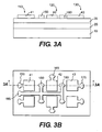
- FIGS. 3A and 3B illustrate a plurality of individual capacitors 110 , 120 , 130 that may be formed from the article resulting from step S170 (FIG. 1).
- the second or top electrode 40 of the capacitor 100 may be photo-etched to form individual top electrodes 41 , 42 , 43 , thereby forming the capacitors 110, 120, 130 .
- the photoetching step can also be used form ground pin pads 150, 160, wire bond pads 155, 165, 175 , and a ground wire bond pad 185 .
- the wire bond pads 155, 165, 175 are used for connection to the individual top electrodes 41, 42, 43 .
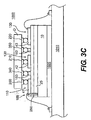
- FIG. 3C is a front elevational view in section of a chip package 1000 .
- the chip package 1000 comprises the article of FIGS. 3A and 3B mounted to a printed wiring board 1010 by an adhesive layer 1020 .
- the capacitors 110 , 120 , 130 are coupled to a device D .
- the electrodes 41, 42, 43 of the capacitors 110, 120, 130 may be connected to individual power pins 200, 210, 220 of the device D using so-called "C4" (controlled collapse chip connect) techniques, for example.
- C4" controlled collapse chip connect
- Ground pins 340, 350 of the device D are similarly connected to the ground pin pads 150, 160, and further connected to the first or bottom electrode 25 by way of a via 250 formed through the wire bond pad 185 , thus completing a low inductance circuit for supplying power to the device D .
- the capacitors 110, 120, 130 on the substrate 10 form an interposer.
- the device D may be, for example, an integrated circuit.
- One or more integrated circuits may be attached to the capacitors 110, 120, 130 on the surface of the ceramic substrate. Other attachment methods may be used such as die attach, flip chip, and wire bonding techniques.
- capacitors for the purposes of illustration, a small number of capacitors, wire bond pads, ground pin pads, and other components are illustrated. Any number of such components, however, can be incorporated into a structure for supplying power to a device, or for other purposes.
- capacitors 110, 120, 130 illustrated above can be attached to printed wiring boards, integrated circuit substrates, or packages using, for example, adhesives.
- wire bonding techniques are illustrated as electrically connecting the capacitors 110, 120, 130 to the printed wiring board (PWB) substrate 1010 .
- PWB printed wiring board
- Other methods of construction and electrical connection to a PWB substrate may also be used, including the use of vias through the ceramic substrate 10 in order to connect electrode and ground pads to the printed wiring board substrate 1010 . This connection can be performed using conductive adhesive or solder in an area array interconnection configuration.
- the top electrodes 110, 120, 130 and the various pads may also be formed by sputtering through a shadow mask, screen-printing or other techniques for providing a directly patterned top electrode structure.
- multilayer capacitors can be fabricated by performing steps S110 through S170 and repeating steps S120 through S170 multiple times. A plurality of individual capacitors can be formed during each process. Multiple capacitor layers are desirable because of the increased total capacitance that can be achieved for a given projected substrate area.
- Additional circuitry can be added to the top of the thin film capacitor interposer structures as described above.
- additional low dielectric constant layers can be added by low-temperature processing, such as spin coating and curing, or by printing and curing polymeric dielectrics such as polyimide or epoxy-based materials. These dielectrics can be metallized and formed into circuit patterns using techniques that are standard in the packaging industry.
- the thin film capacitors made by the methods of the present invention can be further processed into integrated passive devices by addition of other passive components onto the top of the thin film capacitor including inductors, resistors, or other capacitors.
- Inductors are readily formed from the top surface metallization using etching or other patterning techniques known in the art.
- Resistors may be formed using numerous techniques known in the art including sputtering of resistive metals, electroplating, screen printing and curing or firing, and other operations. Numerous integrated passive devices can be formed through the combination of these structures. Such integrated passive devices can be assembled or mounted onto integrated circuit packages or printed wiring boards using known techniques such as flip chip and wire bonding.
- thin-film generally indicates layers having a thickness of less than 2 ⁇ m.
- the above embodiments can have capacitance densities in excess of 1 microFarad/cm 2 .
Landscapes
- Engineering & Computer Science (AREA)
- Power Engineering (AREA)
- Microelectronics & Electronic Packaging (AREA)
- Manufacturing & Machinery (AREA)
- Chemical & Material Sciences (AREA)
- Inorganic Chemistry (AREA)
- Ceramic Capacitors (AREA)
- Parts Printed On Printed Circuit Boards (AREA)
- Fixed Capacitors And Capacitor Manufacturing Machines (AREA)
Description
- The present invention relates to a method of making thin film capacitors, more particularly to thin-film capacitors formed on ceramic substrates.
- As integrated circuits (IC) operate at higher and higher frequencies, noise in the power and ground lines associated with inductance and parasitic capacitance becomes an increasingly important problem. The noise problem requires the use of additional decoupling capacitors in order to provide a stable signal to an IC. Higher operating frequencies combined with lower operating voltages also require that voltage response times to the IC be faster and allowable voltage variations (ripple) be smaller. For example, as a microprocessor begins a calculation, it calls for power. If the response time of the voltage supply is too slow, the microprocessor will experience a voltage drop or power droop that exceeds the allowable ripple voltage and the IC will malfunction. Additionally, as the IC powers up, a slow response time will result in power overshoot. Power droop and overshoot are controlled by the use of capacitors that provide or absorb power within the appropriate response time.
- Capacitors for decoupling and dampening power droop or overshoot are generally placed as close to the IC as possible in order to improve their performance. Conventional designs have capacitors surface mounted on a printed wiring board (PWB) and clustered around the IC. In this arrangement, a large number of capacitors requires complex electrical routing, which leads to inductance. As frequencies increase and operating voltages continue to drop, power increases and higher capacitance must be supplied at increasingly lower inductance levels. Placing the capacitors on the opposite side of the PWB (directly under the IC) reduces inductance somewhat. However, trends in IC size, speed, voltage, power, and packaging mean that conventional approaches will eventually be insufficient in supplying the capacitance within desired inductance and response times.
- U.S. Patent No. 6,477,034 to Chakravorty et al. discloses a capacitor having conductive paths therethrough and providing capacitance between at least two of the conductive paths, the capacitor comprising: a substrate layer; a first conductive layer deposited on the substrate layer, a first portion of the first conductive layer providing a first electrode region; a second conductive layer, a portion of the second conductive layer forming a second electrode region; and a dielectric layer disposed between the first and second conductive layers wherein capacitive regions are formed between the first electrode region and the second electrode region, wherein at least two conductive paths are provided through the substrate layer to provide conductive paths between opposite sides of the capacitor.
- U.S. Patent No. 6,216,324 to Farooq et al. discloses a method for fabricating a thin film multilayer capacitor comprising: providing a multilayer substrate having conductive vias between its top and bottom surfaces; depositing a first level metal structure on the top surface at a thickness of at least 0.5 µm; depositing a thin film dielectric on the first level metal structure; annealing the multilayer substrate at a temperature of approximately 650°C-750°C for one hour in an atmosphere of air, oxygen or nitrogen; patterning the thin film dielectric; applying a first photoresist stencil over the dielectric film such that the stencil patterns areas over the conductive vias on the top surface of the substrate; removing a portion of the thin film dielectric and a portion of the first level metal structure in the exposed areas over the conductive vias; applying a first patterned polyimide layer such that, when a portion of said patterned polyimide layer is subtracted, polyimide insulation structures remain on the top surface adjacent the conductive vias; depositing a second level metal structure; removing a portion of the second level metal structure, applying a second polyimide layer; laser ablating the second polyimide layer in areas over the vias; and depositing solder balls to the top and bottom surfaces of the substrate on the vias.
- Thus, an object of the present invention is to provide capacitor(s) and method(s) for forming capacitor(s) that have desirable electrical and physical properties, such as low inductance and response times.
- According to a first embodiment, a method of making a capacitor comprises providing a ceramic substrate having a first conductive layer. A thin-film dielectric is formed over the first conductive layer, wherein forming the dielectric comprises forming a dielectric layer over the first conductive layer and annealing the dielectric layer at a temperature of at least about 800°C. A temperature in the range of 800-1050°C is preferred. The dielectric resulting from the annealing is re-oxygenated at a temperature in the range of 450-600°C and an oxygen partial pressure in the range of 10-2 to 10-5 atmospheres. A second conductive layer is formed over the dielectric, and the first conductive layer, the dielectric, and the second conductive layer form a capacitor.
- Capacitors constructed according to the above method generally have high capacitance densities and other desirable electrical and physical properties. The capacitors can be, for example, mounted on printed wiring boards and on integrated circuit substrates, and can be used to form integrated circuit packages and integrated passive devices.
Those skilled in the art will appreciate the above stated advantages and other advantages and benefits of various additional embodiments of the invention upon reading the following detailed description of the embodiments with reference to the below-listed drawing. - According to common practice, the various features of the drawings discussed below are not necessarily drawn to scale. Dimensions of various features and elements in the drawings may be expanded or reduced to more clearly illustrate the embodiments of the invention.
-
- FIG. 1 is a block diagram illustrating a method for making a first embodiment of a capacitor;
- FIGS. 2A-2C illustrate steps in forming a capacitor according to the method illustrated in FIG. 1;
- FIG. 3A is a section view taken on
line 3A-3A in FIG. 3B of a plurality of capacitors formed from the capacitor illustrated in FIG. 2C; - FIG. 3B is a top plan view of the capacitors illustrated in FIG. 3A; and
- FIG. 3C is a sectional front elevational view of a chip package having a plurality of the capacitors illustrated in FIGS. 3A and 3B connected to a device D.
- Methods of forming thin-film capacitors on ceramic and glass ceramic-substrates are disclosed. The capacitors are suitable for use as, for example, interposers, integrated passive devices, and for other uses. "Interposer" can refer to, in general, any small substrate containing capacitors or other passive components mounted on a printed wiring board. An interposer having one or more capacitors provides capacitance for decoupling and/or controlling voltage for integrated circuit die mounted on the interposer.
- The interposer embodiments discussed in this specification can include capacitors of high capacitance density. "High capacitance density" generally indicates capacitance densities of at least 1 microFarad/cm2. For the purposes of this specification, ceramic and glass-ceramic substrates are referred to generally as "ceramic substrates."
- High capacitance capacitors on ceramic substrates according to the present embodiments have desirable electrical and physical properties. One desirable electrical property is low inductance because the capacitors can be placed directly beneath an IC. The electrical routing requirements are thereby minimized, considerably reducing loop inductance. One desirable physical property of the ceramic capacitor embodiments is a temperature coefficient of expansion (TCE) value that is between that of an organic printed wiring board (approximately 17 x 10-6/°C) and that of an integrated circuit (approximately 4 x 10⁻⁶/°C). This property provides stress reductions between the IC and the printed wiring board, which enhances long term reliability. Additionally, the temperature coefficient of expansion of the capacitor embodiments can be varied, depending upon the ceramic substrate used, to be closer to that of silicon or to that of an organic printed wiring board.
- FIG. 1 is a block diagram illustrating a method suitable for forming a capacitor on a ceramic substrate according to the present invention.
- FIGS. 2A-2C illustrate manufacturing steps of the capacitor. The method illustrated in FIG. 1 and discussed in detail below addresses the formation of a single capacitor on a ceramic substrate. Several capacitors can be formed in a batch mode, however, using the method illustrated in FIGS. 1 and 2A-2C.
- Referring to FIGS. 1 and 2A, in step S110, a thin-film grade
ceramic substrate 10 having asmooth surface 12 is cleaned to remove organic or other impurities that may have detrimental effects on capacitor performance. If thesubstrate 10 has arough surface 12, smoothening or polishing of the substrate surface to ensure a uniform and flat surface on which to form the thin-film electrode and dielectric layers may be performed as part of the cleaning process. As an alternative to polishing, a substrate with a rough surface may be planarized by coating and annealing one or more layers of dielectric precursor solution on thesubstrate 10surface 12 prior to forming a first conductive electrode layer. - The
substrate 10 may have a temperature coefficient of expansion that is similar to a BaTiO3-based dielectric layer to be deposited over thesubstrate 10. Examples of such substrates include magnesia (MgO), alumina (Al2O3), barium titanate (BaTiO3), strontium titanate (SrTiO3), magnesium aluminate (MgAl2O4), yttria stabilized zirconia (ZrO2) or glass-ceramic substrates such as any commercial low temperature co-fired ceramic substrates using precious or base metal metallization, or any commercial high temperature co-fired ceramic system using tungsten or molybdenum metallization. Use of such substrates ensures that a dielectric film will not experience large stresses when cooling down from annealing processes. Large stresses are undesirable because they may induce cracking in the dielectric film. - In step S120, a first
conductive layer 20 is formed over theceramic substrate 10. The firstconductive layer 20 is used to form a first electrode of the finished capacitor. The firstconductive layer 20 can cover all or part of thesubstrate 10. The firstconductive layer 20 may comprise one or more precious metal such as platinum, palladium, gold and silver, or one or more base metal such as copper, nickel, manganese, molybdenum and tungsten. It can be formed by a deposition process such as sputtering or evaporation. When the firstconductive layer 20 is deposited by sputtering or evaporation, a thin layer (e.g. of the order of about 20 Angstroms thickness) of an adhesion enhancing material may be deposited over thesubstrate 10 before depositing themetal layer 20. Titanium is one example of an adhesion enhancing material. The firstconductive layer 20 may also be formed by printing a thick-film metal paste composition or an organo-metallic material. If a co-firedceramic substrate 10 is used, a first electrode may already be present as part of the substrate and step S120 may be dispensed with or bypassed. - In step S130, a
dielectric precursor layer 30 is formed over the firstconductive layer 20. Theprecursor layer 30 will form the dielectric of the resultant capacitor, and may be formed by depositing a precursor solution over the firstconductive layer 20. The precursor solution may comprise precursor chemicals for forming thin-film crystalline barium titanate (BaTiO3) layers, and chemical solution deposition (CSD) techniques may be used to form theprecursor layer 30. CSD techniques are desirable due to their simplicity and low cost. A chemical precursor solution used to form an undoped (or "pure") BaTiO3 dielectric may contain barium acetate and titanium isopropoxide. Chemicals such as acetylacetone, acetic acid and methanol may be used to dissolve the precursor components and to stabilize the precursor solution. - Dopant cations may be added to a BaTiO3 precursor solution in orderto modify its dielectric characteristics. Transition metal cations, for example, can be included. Transition metal cations with the oxide stoichiometry MO2, where M is the transition metal cation (e.g., Zr, Hf, Sn, Ce), may be added to smooth the temperature dependence of the resulting capacitance by shifting the temperatures of the three phase transitions of BaTiO3 closer to one another. Metal cations with the oxide stoichiometry MO, where M is an alkaline earth metal (e.g., Ca, Sr, Mg), may be added shift the dielectric Curie point to lower temperatures. Such MO and MO2 dopants are useful for improving the temperature stability of the resultant capacitor. Rare earth cations having the oxide stoichiometry R2O3, where R is a rare earth cation (e.g., Y, Ho, Dy, La, Eu), may be added to chemically compensate for oxygen loss that may occur in the
precursor layer 30 during a low oxygen partial pressure anneal. Transition metal cations with multiple preferred valence states such as Mn may also be added for their ability to chemically compensate for oxygen loss. Such dopants are particularly useful for maintaining high insulation resistance in capacitors that use base metal electrodes, such as copper. - Dopants or mixtures thereof may be used in concentrations of between about 0 and 30 mol percent in the precursor solution. The specific combination of dopants and mixtures will depend upon the desired combination of dielectric properties, transport properties, and temperature dependent properties for the resulting dielectric.
- The following chemicals may be used to supply cations in doped precursor compositions:
- Mn: manganese acetate tetrahydrate
- Y: yttrium acetate hydrate
- Zr: zirconium propoxide
- Ca: calcium acetate hydrate
- Sr: strontium acetate hydrate
- Ho: holmium acetate hydrate
- Dy: dysprosium acetate hydrate
- Hf: hafnium chloride
- Fe: Iron acetate
- Mg: magnesium acetate tetrahydrate.
- In step S140, the
precursor layer 30 is dried to remove solvent. If athicker precursor layer 30 is desired, steps S130 and S140 are repeated until a desired precursor layer thickness is attained. Referring to FIG. 1, in step S150, the resulting article is annealed. Annealing is performed at a temperature of at least 800°C, which removes residual organic material, and then densifies and crystallizes the drieddielectric precursor layer 30. Referring to FIG. 2B, a dielectric 35 and afirst electrode 25 result from the annealing process. The resultingdielectric 35 thickness may be in the range of about 0.2-2.0 microns (µm). The resulting article is then allowed to cool in step S160. - When using a precious metal such as platinum to form the
first electrode 25, annealing may be conducted in a high temperature air furnace. When using a base metal such as copper to form thefirst electrode 25, annealing may be conducted in a low oxygen partial pressure environment, i.e. less than 10-6 atmospheres. Oxidation of abase metal layer 20 is avoided by selecting an appropriate low oxygen partial pressure for the annealing temperature and the metal combination from phase stability diagrams. For example, if using copper electrodes, and annealing at about 900°C, the oxygen partial pressure should be less than 10-8 atmospheres. Optionally, annealing may be effected in a nitrogen atmosphere. - In the case of a copper
first electrode 25, the low oxygen partial pressure annealing will not oxidize the copper to Cu2O or CuO. The reduced oxygen partial pressures combined with higher annealing temperatures, such as annealing temperatures of at least 800°C, however, may yield a dielectric 35 with an increased concentration of oxygen vacancies, resulting in a reduced dielectric insulation resistance. The dielectric 35 may therefore require aleovalent cation doping, and a re-oxygenation process is effected. The dopants compensate for oxygen loss that may occur during the low oxygen pressure anneal, and after the re-oxygenation process yields a dielectric 35 with good insulation resistance. Such dopants include, for example, Mn, Y, Ho, and Dy. - Re-oxygenation is effected at a partial pressure of oxygen of between 10-5 and 10-2 atmospheres at a temperature in the range of 450-600°C, corresponding to a short anneal at a lower temperature and at a higher oxygen pressure that is not sufficient to significantly oxidize the
first electrode 25. Such a re-oxygenation may be effected for a few minutes at a temperature of, e.g. 500°C. Re-oxygenation can be integrated into the cooldown step S160 of the high temperature anneal, or performed as a separate process. - Referring to FIG. 2C, in step S170 (FIG. 1), a second or
top electrode 40 is formed over the resultingdielectric 35. The second ortop electrode 40 can be formed by, for example, sputtering, evaporation, combustion vapor deposition, electroless plating, printing or other suitable deposition methods, and may be followed by plating to a specific thickness in order to obtain desired electrical properties. Acapacitor 100 is formed by the addition of thetop electrode 40. - FIGS. 3A and 3B illustrate a plurality of
individual capacitors top electrode 40 of thecapacitor 100 may be photo-etched to form individualtop electrodes capacitors ground pin pads wire bond pads wire bond pad 185. Thewire bond pads top electrodes - FIG. 3C is a front elevational view in section of a
chip package 1000. Thechip package 1000 comprises the article of FIGS. 3A and 3B mounted to a printedwiring board 1010 by anadhesive layer 1020. Thecapacitors electrodes capacitors ground pin pads bottom electrode 25 by way of a via 250 formed through thewire bond pad 185, thus completing a low inductance circuit for supplying power to the device D . Thecapacitors substrate 10 form an interposer. - The device D may be, for example, an integrated circuit. One or more integrated circuits may be attached to the
capacitors - In the above embodiment, for the purposes of illustration, a small number of capacitors, wire bond pads, ground pin pads, and other components are illustrated. Any number of such components, however, can be incorporated into a structure for supplying power to a device, or for other purposes.
- These
capacitors capacitors substrate 1010. Other methods of construction and electrical connection to a PWB substrate may also be used, including the use of vias through theceramic substrate 10 in order to connect electrode and ground pads to the printedwiring board substrate 1010. This connection can be performed using conductive adhesive or solder in an area array interconnection configuration. - The
top electrodes - If desired, multilayer capacitors can be fabricated by performing steps S110 through S170 and repeating steps S120 through S170 multiple times. A plurality of individual capacitors can be formed during each process. Multiple capacitor layers are desirable because of the increased total capacitance that can be achieved for a given projected substrate area.
- Additional circuitry can be added to the top of the thin film capacitor interposer structures as described above. For example, additional low dielectric constant layers can be added by low-temperature processing, such as spin coating and curing, or by printing and curing polymeric dielectrics such as polyimide or epoxy-based materials. These dielectrics can be metallized and formed into circuit patterns using techniques that are standard in the packaging industry.
- The thin film capacitors made by the methods of the present invention can be further processed into integrated passive devices by addition of other passive components onto the top of the thin film capacitor including inductors, resistors, or other capacitors. Inductors are readily formed from the top surface metallization using etching or other patterning techniques known in the art. Resistors may be formed using numerous techniques known in the art including sputtering of resistive metals, electroplating, screen printing and curing or firing, and other operations. Numerous integrated passive devices can be formed through the combination of these structures. Such integrated passive devices can be assembled or mounted onto integrated circuit packages or printed wiring boards using known techniques such as flip chip and wire bonding.
- The term "thin-film" generally indicates layers having a thickness of less than 2 µm. The above embodiments can have capacitance densities in excess of 1 microFarad/cm2.
- The foregoing description of the invention illustrates and describes the present invention. Additionally, the disclosure describes only selected preferred embodiments of the invention, but it is to be understood that the invention is capable of changes or modifications within the scope of the inventive concept as defined by the appended claims, commensurate with the above teachings, and/or within the skill or knowledge of the relevant art.
- The description is not intended to limit the invention to the form disclosed herein. Also, it is intended that the appended claims be construed to include alternative embodiments, not explicitly defined in the detailed description.
Claims (17)
- A method of making one or more thin-film capacitor on a substrate, comprising:providing a ceramic substrate having a first conductive layer thereon;forming a layer of dielectric over the first conductive layer;annealing at a temperature of at least about 800°C;re-oxygenating the dielectric resulting from the annealing at a temperature in the range of 450-600°C and an oxygen partial pressure in the range of 10-2 to 10-5 atmospheres; andforming a second conductive layer over the dielectric.
- The method of claim 1, wherein the substrate is provided by forming the first conductive layer over a ceramic substrate material.
- The method of claim 1 or claim 2, wherein annealing results in a dielectric comprising crystalline barium titanate.
- The method of any preceding claim, wherein the annealing is effected at a temperature in the range of 800-1050°C.
- The method of any preceding claim, wherein the first conductive layer comprises at least one metal selected from nickel, copper, manganese, molybdenum and tungsten.
- The method of claim 5, wherein the annealing is effected in an environment having an oxygen partial pressure of less than 10-6 atmospheres.
- The method of any preceding claim, wherein the annealing is effected in a nitrogen atmosphere.
- The method of any of claims 1 to 4, wherein the first conductive layer comprises at least one metal selected from platinum, palladium, gold and silver.
- The method of claim 8 wherein the annealing takes place in air.
- The method of any preceding claim, wherein forming the layer of dielectric comprises:providing a dielectric precursor solution; anddepositing the dielectric precursor solution over the first conductive layer.
- The method of any preceding claim, wherein the dielectric is a doped dielectric.
- The method of any preceding claim, wherein the layer of dielectric has a thickness in the range of about 0.2-2.0 microns.
- The method of any preceding claim, wherein forming the second conductive layer comprises:sputtering a conductive layer over the dielectric; andplating the conductive layer with a conductive material.
- The method of any preceding claim, wherein the substrate comprises at least one material selected from magnesia, alumina, glass-ceramic, zirconia, magnesium aluminate, strontium titanate and barium titanate.
- The method of any preceding claim, further comprising:forming a plurality of electrodes from the second electrode layer, thereby forming a plurality of capacitors.
- The method of any preceding claim further comprising mounting said capacitor on a printed wiring board.
- The method of any preceding claim further comprising mounting said capacitor on an integrated circuit substrate.
Applications Claiming Priority (4)
| Application Number | Priority Date | Filing Date | Title |
|---|---|---|---|
| US53319503P | 2003-12-30 | 2003-12-30 | |
| US533195P | 2003-12-30 | ||
| US5350 | 2004-12-06 | ||
| US11/005,350 US7256980B2 (en) | 2003-12-30 | 2004-12-06 | Thin film capacitors on ceramic |
Publications (2)
| Publication Number | Publication Date |
|---|---|
| EP1551041A1 EP1551041A1 (en) | 2005-07-06 |
| EP1551041B1 true EP1551041B1 (en) | 2007-03-07 |
Family
ID=34576103
Family Applications (1)
| Application Number | Title | Priority Date | Filing Date |
|---|---|---|---|
| EP04257903A Expired - Lifetime EP1551041B1 (en) | 2003-12-30 | 2004-12-17 | Method of making thin film capacitors on ceramic substrate |
Country Status (7)
| Country | Link |
|---|---|
| US (1) | US7256980B2 (en) |
| EP (1) | EP1551041B1 (en) |
| JP (1) | JP2005210090A (en) |
| KR (1) | KR100680107B1 (en) |
| CN (1) | CN1637973A (en) |
| DE (1) | DE602004005145T2 (en) |
| TW (1) | TW200527456A (en) |
Cited By (1)
| Publication number | Priority date | Publication date | Assignee | Title |
|---|---|---|---|---|
| US7818855B2 (en) | 2006-11-10 | 2010-10-26 | E. I. Du Pont De Nemours And Company | Method of making thin-film capacitors on metal foil using thick top electrodes |
Families Citing this family (19)
| Publication number | Priority date | Publication date | Assignee | Title |
|---|---|---|---|---|
| JP4983134B2 (en) * | 2005-07-29 | 2012-07-25 | Tdk株式会社 | Dielectric film manufacturing method and capacitor |
| US7539005B2 (en) * | 2005-07-29 | 2009-05-26 | Tdk Corporation | Dielectric film production process and capacitor |
| JP4956939B2 (en) | 2005-08-31 | 2012-06-20 | Tdk株式会社 | Dielectric film and manufacturing method thereof |
| JP4670612B2 (en) * | 2005-11-30 | 2011-04-13 | Tdk株式会社 | Dielectric element and manufacturing method thereof |
| US7531416B2 (en) * | 2005-12-21 | 2009-05-12 | E. I. Du Pont De Nemours And Company | Thick film capacitors on ceramic interconnect substrates |
| US20080001271A1 (en) * | 2006-06-30 | 2008-01-03 | Sony Ericsson Mobile Communications Ab | Flipped, stacked-chip IC packaging for high bandwidth data transfer buses |
| US20080010798A1 (en) * | 2006-07-14 | 2008-01-17 | Borland William J | Thin film dielectrics with co-fired electrodes for capacitors and methods of making thereof |
| US20080037198A1 (en) * | 2006-08-10 | 2008-02-14 | Borland William J | Methods of forming individual formed-on-foil thin capacitors for embedding inside printed wiring boards and semiconductor packages |
| US7841075B2 (en) * | 2007-06-19 | 2010-11-30 | E. I. Du Pont De Nemours And Company | Methods for integration of thin-film capacitors into the build-up layers of a PWB |
| US8084841B2 (en) * | 2009-05-05 | 2011-12-27 | Georgia Tech Research | Systems and methods for providing high-density capacitors |
| US20100284123A1 (en) * | 2009-05-05 | 2010-11-11 | Pulugurtha Markondeyaraj | Systems and methods for fabricating high-density capacitors |
| WO2014081917A2 (en) * | 2012-11-21 | 2014-05-30 | 3M Innovative Properties Company | Multilayer film including first and second dielectric layers |
| CN104937685A (en) * | 2012-11-21 | 2015-09-23 | 3M创新有限公司 | Multilayer film including a first dielectric layer and a second dielectric layer |
| CN103219318B (en) * | 2013-04-12 | 2015-07-08 | 中国电子科技集团公司第十三研究所 | High-temperature-resistant MIM capacitor for microwave internal matching transistor and manufacturing method thereof |
| CN105261657B (en) * | 2015-10-30 | 2018-05-11 | 中国振华集团云科电子有限公司 | A kind of manufacturing process of MIS thin film capacitors |
| WO2017127995A1 (en) * | 2016-01-25 | 2017-08-03 | Schott Glass Technologies (Suzhou) Co. Ltd. | Article with high capacity per area and use of such article in finger-print sensors |
| CN106158373A (en) * | 2016-08-01 | 2016-11-23 | 合肥佳瑞林电子技术有限公司 | A kind of preparation method of thin film capacitor |
| US10760156B2 (en) | 2017-10-13 | 2020-09-01 | Honeywell International Inc. | Copper manganese sputtering target |
| US11035036B2 (en) | 2018-02-01 | 2021-06-15 | Honeywell International Inc. | Method of forming copper alloy sputtering targets with refined shape and microstructure |
Family Cites Families (29)
| Publication number | Priority date | Publication date | Assignee | Title |
|---|---|---|---|---|
| DE3138177A1 (en) * | 1981-09-25 | 1983-04-14 | Philips Patentverwaltung Gmbh, 2000 Hamburg | "METHOD FOR PRODUCING A DIELECTRIC" |
| US4870539A (en) | 1989-01-17 | 1989-09-26 | International Business Machines Corporation | Doped titanate glass-ceramic for grain boundary barrier layer capacitors |
| US5198269A (en) * | 1989-04-24 | 1993-03-30 | Battelle Memorial Institute | Process for making sol-gel deposited ferroelectric thin films insensitive to their substrates |
| WO1992019564A1 (en) * | 1991-05-01 | 1992-11-12 | The Regents Of The University Of California | Amorphous ferroelectric materials |
| US5614018A (en) * | 1991-12-13 | 1997-03-25 | Symetrix Corporation | Integrated circuit capacitors and process for making the same |
| US5271955A (en) * | 1992-04-06 | 1993-12-21 | Motorola, Inc. | Method for making a semiconductor device having an anhydrous ferroelectric thin film |
| US5348894A (en) * | 1993-01-27 | 1994-09-20 | Texas Instruments Incorporated | Method of forming electrical connections to high dielectric constant materials |
| US5384294A (en) * | 1993-11-30 | 1995-01-24 | The United States Of America As Represented By The Secretary Of The Air Force | Sol-gel derived lead oxide containing ceramics |
| US5663088A (en) * | 1995-05-19 | 1997-09-02 | Micron Technology, Inc. | Method of forming a Ta2 O5 dielectric layer with amorphous diffusion barrier layer and method of forming a capacitor having a Ta2 O5 dielectric layer and amorphous diffusion barrier layer |
| US6066581A (en) * | 1995-07-27 | 2000-05-23 | Nortel Networks Corporation | Sol-gel precursor and method for formation of ferroelectric materials for integrated circuits |
| JP3481807B2 (en) * | 1995-12-13 | 2003-12-22 | 京セラ株式会社 | Dielectric thin film and ceramic capacitor |
| US5843830A (en) * | 1996-06-26 | 1998-12-01 | Micron Technology, Inc. | Capacitor, and methods for forming a capacitor |
| US5912044A (en) * | 1997-01-10 | 1999-06-15 | International Business Machines Corporation | Method for forming thin film capacitors |
| US5910880A (en) * | 1997-08-20 | 1999-06-08 | Micron Technology, Inc. | Semiconductor circuit components and capacitors |
| US5962654A (en) * | 1998-01-30 | 1999-10-05 | International Business Machines Operation | Alkoxyalkoxides and use to form films |
| US6023407A (en) * | 1998-02-26 | 2000-02-08 | International Business Machines Corporation | Structure for a thin film multilayer capacitor |
| KR100465140B1 (en) * | 1999-11-02 | 2005-01-13 | 티디케이가부시기가이샤 | Multilayer capacitor |
| US6727143B1 (en) * | 1999-11-30 | 2004-04-27 | Advanced Micro Devices, Inc. | Method and system for reducing charge gain and charge loss when using an ARC layer in interlayer dielectric formation |
| US6339527B1 (en) * | 1999-12-22 | 2002-01-15 | International Business Machines Corporation | Thin film capacitor on ceramic |
| US6404615B1 (en) * | 2000-02-16 | 2002-06-11 | Intarsia Corporation | Thin film capacitors |
| US6611419B1 (en) * | 2000-07-31 | 2003-08-26 | Intel Corporation | Electronic assembly comprising substrate with embedded capacitors |
| US6541137B1 (en) * | 2000-07-31 | 2003-04-01 | Motorola, Inc. | Multi-layer conductor-dielectric oxide structure |
| JP2002260958A (en) * | 2000-12-28 | 2002-09-13 | Matsushita Electric Ind Co Ltd | Plate-shaped capacitor, method of manufacturing the same, and chip-size package using the capacitor |
| JP2002231575A (en) * | 2001-01-31 | 2002-08-16 | Kyocera Corp | Thin film capacitors and capacitor substrates |
| JP2003045742A (en) * | 2001-07-26 | 2003-02-14 | Kyocera Corp | Thin film capacitors |
| US6477034B1 (en) * | 2001-10-03 | 2002-11-05 | Intel Corporation | Interposer substrate with low inductance capacitive paths |
| JP3986859B2 (en) * | 2002-03-25 | 2007-10-03 | 富士通株式会社 | Thin film capacitor and manufacturing method thereof |
| US6818469B2 (en) * | 2002-05-27 | 2004-11-16 | Nec Corporation | Thin film capacitor, method for manufacturing the same and printed circuit board incorporating the same |
| US7029971B2 (en) * | 2003-07-17 | 2006-04-18 | E. I. Du Pont De Nemours And Company | Thin film dielectrics for capacitors and methods of making thereof |
-
2004
- 2004-12-06 US US11/005,350 patent/US7256980B2/en not_active Expired - Lifetime
- 2004-12-17 DE DE602004005145T patent/DE602004005145T2/en not_active Expired - Lifetime
- 2004-12-17 EP EP04257903A patent/EP1551041B1/en not_active Expired - Lifetime
- 2004-12-17 JP JP2004366464A patent/JP2005210090A/en active Pending
- 2004-12-23 TW TW093140169A patent/TW200527456A/en unknown
- 2004-12-30 KR KR1020040116144A patent/KR100680107B1/en not_active Expired - Fee Related
- 2004-12-30 CN CNA2004100116540A patent/CN1637973A/en active Pending
Cited By (1)
| Publication number | Priority date | Publication date | Assignee | Title |
|---|---|---|---|---|
| US7818855B2 (en) | 2006-11-10 | 2010-10-26 | E. I. Du Pont De Nemours And Company | Method of making thin-film capacitors on metal foil using thick top electrodes |
Also Published As
| Publication number | Publication date |
|---|---|
| DE602004005145D1 (en) | 2007-04-19 |
| US7256980B2 (en) | 2007-08-14 |
| KR100680107B1 (en) | 2007-02-08 |
| US20050141171A1 (en) | 2005-06-30 |
| KR20050069913A (en) | 2005-07-05 |
| CN1637973A (en) | 2005-07-13 |
| EP1551041A1 (en) | 2005-07-06 |
| TW200527456A (en) | 2005-08-16 |
| DE602004005145T2 (en) | 2007-12-13 |
| JP2005210090A (en) | 2005-08-04 |
Similar Documents
| Publication | Publication Date | Title |
|---|---|---|
| US7256980B2 (en) | Thin film capacitors on ceramic | |
| US7557014B2 (en) | Semiconductor system-in-package | |
| CN100505124C (en) | Film capacitor, built-in high-density assembled substrate thereof and method for making said film capacitor | |
| EP0070380B1 (en) | Discrete thin film capacitor | |
| KR100324209B1 (en) | Fabrication method of silver inductors | |
| JP2005039282A (en) | Thin film dielectric for capacitor and manufacturing method thereof | |
| US7026680B2 (en) | Thin film capacitive element, method for producing same and electronic device | |
| CN101524003A (en) | Power core device and manufacturing method thereof | |
| KR20090057922A (en) | Improved Intermediate Frequency Decoupling Method | |
| US5070393A (en) | Aluminum nitride substrate for formation of thin-film conductor layer and semiconductor device using the substrate | |
| JPH06333740A (en) | Composite integrated circuit component | |
| CN1953169A (en) | Power core devices and methods of making thereof | |
| US7531416B2 (en) | Thick film capacitors on ceramic interconnect substrates | |
| US6503609B1 (en) | Passive ceramic component | |
| JP4876518B2 (en) | Manufacturing method of electronic parts | |
| US7818855B2 (en) | Method of making thin-film capacitors on metal foil using thick top electrodes | |
| JP2001250885A (en) | Circuit board with built-in capacitor and semiconductor device using the same | |
| JP2000252163A (en) | Capacitors | |
| JP3692258B2 (en) | Capacitor | |
| JP2000150290A (en) | Capacitor | |
| JP4022105B2 (en) | Manufacturing method of multilayer wiring board | |
| JP2000311832A (en) | Thin film capacitors and substrates | |
| JP2000306767A (en) | Thin film capacitor, multilayer laminated mounting substrate, and method of manufacturing thin film capacitor | |
| JP2001023851A (en) | Capacitor integrated ceramic sintered body and method of manufacturing the same | |
| KR100515679B1 (en) | Low-temperature co-firing ceramic meterials |
Legal Events
| Date | Code | Title | Description |
|---|---|---|---|
| PUAI | Public reference made under article 153(3) epc to a published international application that has entered the european phase |
Free format text: ORIGINAL CODE: 0009012 |
|
| AK | Designated contracting states |
Kind code of ref document: A1 Designated state(s): AT BE BG CH CY CZ DE DK EE ES FI FR GB GR HU IE IS IT LI LT LU MC NL PL PT RO SE SI SK TR |
|
| AX | Request for extension of the european patent |
Extension state: AL BA HR LV MK YU |
|
| 17P | Request for examination filed |
Effective date: 20051206 |
|
| AKX | Designation fees paid |
Designated state(s): DE FR GB |
|
| RTI1 | Title (correction) |
Free format text: METHOD OF MAKING THIN FILM CAPACITORS ON CERAMIC SUBSTRATE |
|
| GRAP | Despatch of communication of intention to grant a patent |
Free format text: ORIGINAL CODE: EPIDOSNIGR1 |
|
| GRAS | Grant fee paid |
Free format text: ORIGINAL CODE: EPIDOSNIGR3 |
|
| GRAA | (expected) grant |
Free format text: ORIGINAL CODE: 0009210 |
|
| AK | Designated contracting states |
Kind code of ref document: B1 Designated state(s): DE FR GB |
|
| REG | Reference to a national code |
Ref country code: GB Ref legal event code: FG4D |
|
| REF | Corresponds to: |
Ref document number: 602004005145 Country of ref document: DE Date of ref document: 20070419 Kind code of ref document: P |
|
| PLBE | No opposition filed within time limit |
Free format text: ORIGINAL CODE: 0009261 |
|
| STAA | Information on the status of an ep patent application or granted ep patent |
Free format text: STATUS: NO OPPOSITION FILED WITHIN TIME LIMIT |
|
| 26N | No opposition filed |
Effective date: 20071210 |
|
| PGFP | Annual fee paid to national office [announced via postgrant information from national office to epo] |
Ref country code: FR Payment date: 20091221 Year of fee payment: 6 Ref country code: GB Payment date: 20091216 Year of fee payment: 6 |
|
| PGFP | Annual fee paid to national office [announced via postgrant information from national office to epo] |
Ref country code: DE Payment date: 20091222 Year of fee payment: 6 |
|
| GBPC | Gb: european patent ceased through non-payment of renewal fee |
Effective date: 20101217 |
|
| REG | Reference to a national code |
Ref country code: FR Ref legal event code: ST Effective date: 20110831 |
|
| PG25 | Lapsed in a contracting state [announced via postgrant information from national office to epo] |
Ref country code: FR Free format text: LAPSE BECAUSE OF NON-PAYMENT OF DUE FEES Effective date: 20110103 |
|
| REG | Reference to a national code |
Ref country code: DE Ref legal event code: R119 Ref document number: 602004005145 Country of ref document: DE Effective date: 20110701 |
|
| PG25 | Lapsed in a contracting state [announced via postgrant information from national office to epo] |
Ref country code: DE Free format text: LAPSE BECAUSE OF NON-PAYMENT OF DUE FEES Effective date: 20110701 Ref country code: GB Free format text: LAPSE BECAUSE OF NON-PAYMENT OF DUE FEES Effective date: 20101217 |