EP1550078B1 - Rfid-fähige gerillte strukturen - Google Patents
Rfid-fähige gerillte strukturen Download PDFInfo
- Publication number
- EP1550078B1 EP1550078B1 EP03798322A EP03798322A EP1550078B1 EP 1550078 B1 EP1550078 B1 EP 1550078B1 EP 03798322 A EP03798322 A EP 03798322A EP 03798322 A EP03798322 A EP 03798322A EP 1550078 B1 EP1550078 B1 EP 1550078B1
- Authority
- EP
- European Patent Office
- Prior art keywords
- processor
- linerboard
- corrugated medium
- corrugated
- inlet
- Prior art date
- Legal status (The legal status is an assumption and is not a legal conclusion. Google has not performed a legal analysis and makes no representation as to the accuracy of the status listed.)
- Revoked
Links
Images


Classifications
-
- G—PHYSICS
- G06—COMPUTING OR CALCULATING; COUNTING
- G06K—GRAPHICAL DATA READING; PRESENTATION OF DATA; RECORD CARRIERS; HANDLING RECORD CARRIERS
- G06K19/00—Record carriers for use with machines and with at least a part designed to carry digital markings
- G06K19/02—Record carriers for use with machines and with at least a part designed to carry digital markings characterised by the selection of materials, e.g. to avoid wear during transport through the machine
-
- B—PERFORMING OPERATIONS; TRANSPORTING
- B31—MAKING ARTICLES OF PAPER, CARDBOARD OR MATERIAL WORKED IN A MANNER ANALOGOUS TO PAPER; WORKING PAPER, CARDBOARD OR MATERIAL WORKED IN A MANNER ANALOGOUS TO PAPER
- B31F—MECHANICAL WORKING OR DEFORMATION OF PAPER, CARDBOARD OR MATERIAL WORKED IN A MANNER ANALOGOUS TO PAPER
- B31F1/00—Mechanical deformation without removing material, e.g. in combination with laminating
- B31F1/20—Corrugating; Corrugating combined with laminating to other layers
- B31F1/24—Making webs in which the channel of each corrugation is transverse to the web feed
- B31F1/26—Making webs in which the channel of each corrugation is transverse to the web feed by interengaging toothed cylinders cylinder constructions
- B31F1/28—Making webs in which the channel of each corrugation is transverse to the web feed by interengaging toothed cylinders cylinder constructions combined with uniting the corrugated webs to flat webs ; Making double-faced corrugated cardboard
- B31F1/2822—Making webs in which the channel of each corrugation is transverse to the web feed by interengaging toothed cylinders cylinder constructions combined with uniting the corrugated webs to flat webs ; Making double-faced corrugated cardboard involving additional operations
-
- G—PHYSICS
- G06—COMPUTING OR CALCULATING; COUNTING
- G06K—GRAPHICAL DATA READING; PRESENTATION OF DATA; RECORD CARRIERS; HANDLING RECORD CARRIERS
- G06K19/00—Record carriers for use with machines and with at least a part designed to carry digital markings
- G06K19/06—Record carriers for use with machines and with at least a part designed to carry digital markings characterised by the kind of the digital marking, e.g. shape, nature, code
- G06K19/067—Record carriers with conductive marks, printed circuits or semiconductor circuit elements, e.g. credit or identity cards also with resonating or responding marks without active components
- G06K19/07—Record carriers with conductive marks, printed circuits or semiconductor circuit elements, e.g. credit or identity cards also with resonating or responding marks without active components with integrated circuit chips
- G06K19/077—Constructional details, e.g. mounting of circuits in the carrier
- G06K19/07745—Mounting details of integrated circuit chips
-
- G—PHYSICS
- G06—COMPUTING OR CALCULATING; COUNTING
- G06K—GRAPHICAL DATA READING; PRESENTATION OF DATA; RECORD CARRIERS; HANDLING RECORD CARRIERS
- G06K19/00—Record carriers for use with machines and with at least a part designed to carry digital markings
- G06K19/06—Record carriers for use with machines and with at least a part designed to carry digital markings characterised by the kind of the digital marking, e.g. shape, nature, code
- G06K19/067—Record carriers with conductive marks, printed circuits or semiconductor circuit elements, e.g. credit or identity cards also with resonating or responding marks without active components
- G06K19/07—Record carriers with conductive marks, printed circuits or semiconductor circuit elements, e.g. credit or identity cards also with resonating or responding marks without active components with integrated circuit chips
- G06K19/077—Constructional details, e.g. mounting of circuits in the carrier
- G06K19/07749—Constructional details, e.g. mounting of circuits in the carrier the record carrier being capable of non-contact communication, e.g. constructional details of the antenna of a non-contact smart card
-
- Y—GENERAL TAGGING OF NEW TECHNOLOGICAL DEVELOPMENTS; GENERAL TAGGING OF CROSS-SECTIONAL TECHNOLOGIES SPANNING OVER SEVERAL SECTIONS OF THE IPC; TECHNICAL SUBJECTS COVERED BY FORMER USPC CROSS-REFERENCE ART COLLECTIONS [XRACs] AND DIGESTS
- Y10—TECHNICAL SUBJECTS COVERED BY FORMER USPC
- Y10S—TECHNICAL SUBJECTS COVERED BY FORMER USPC CROSS-REFERENCE ART COLLECTIONS [XRACs] AND DIGESTS
- Y10S206/00—Special receptacle or package
- Y10S206/807—Tamper proof
-
- Y—GENERAL TAGGING OF NEW TECHNOLOGICAL DEVELOPMENTS; GENERAL TAGGING OF CROSS-SECTIONAL TECHNOLOGIES SPANNING OVER SEVERAL SECTIONS OF THE IPC; TECHNICAL SUBJECTS COVERED BY FORMER USPC CROSS-REFERENCE ART COLLECTIONS [XRACs] AND DIGESTS
- Y10—TECHNICAL SUBJECTS COVERED BY FORMER USPC
- Y10T—TECHNICAL SUBJECTS COVERED BY FORMER US CLASSIFICATION
- Y10T156/00—Adhesive bonding and miscellaneous chemical manufacture
- Y10T156/10—Methods of surface bonding and/or assembly therefor
- Y10T156/1002—Methods of surface bonding and/or assembly therefor with permanent bending or reshaping or surface deformation of self sustaining lamina
- Y10T156/1007—Running or continuous length work
- Y10T156/1016—Transverse corrugating
-
- Y—GENERAL TAGGING OF NEW TECHNOLOGICAL DEVELOPMENTS; GENERAL TAGGING OF CROSS-SECTIONAL TECHNOLOGIES SPANNING OVER SEVERAL SECTIONS OF THE IPC; TECHNICAL SUBJECTS COVERED BY FORMER USPC CROSS-REFERENCE ART COLLECTIONS [XRACs] AND DIGESTS
- Y10—TECHNICAL SUBJECTS COVERED BY FORMER USPC
- Y10T—TECHNICAL SUBJECTS COVERED BY FORMER US CLASSIFICATION
- Y10T156/00—Adhesive bonding and miscellaneous chemical manufacture
- Y10T156/10—Methods of surface bonding and/or assembly therefor
- Y10T156/1052—Methods of surface bonding and/or assembly therefor with cutting, punching, tearing or severing
-
- Y—GENERAL TAGGING OF NEW TECHNOLOGICAL DEVELOPMENTS; GENERAL TAGGING OF CROSS-SECTIONAL TECHNOLOGIES SPANNING OVER SEVERAL SECTIONS OF THE IPC; TECHNICAL SUBJECTS COVERED BY FORMER USPC CROSS-REFERENCE ART COLLECTIONS [XRACs] AND DIGESTS
- Y10—TECHNICAL SUBJECTS COVERED BY FORMER USPC
- Y10T—TECHNICAL SUBJECTS COVERED BY FORMER US CLASSIFICATION
- Y10T156/00—Adhesive bonding and miscellaneous chemical manufacture
- Y10T156/12—Surface bonding means and/or assembly means with cutting, punching, piercing, severing or tearing
-
- Y—GENERAL TAGGING OF NEW TECHNOLOGICAL DEVELOPMENTS; GENERAL TAGGING OF CROSS-SECTIONAL TECHNOLOGIES SPANNING OVER SEVERAL SECTIONS OF THE IPC; TECHNICAL SUBJECTS COVERED BY FORMER USPC CROSS-REFERENCE ART COLLECTIONS [XRACs] AND DIGESTS
- Y10—TECHNICAL SUBJECTS COVERED BY FORMER USPC
- Y10T—TECHNICAL SUBJECTS COVERED BY FORMER US CLASSIFICATION
- Y10T428/00—Stock material or miscellaneous articles
- Y10T428/13—Hollow or container type article [e.g., tube, vase, etc.]
- Y10T428/1303—Paper containing [e.g., paperboard, cardboard, fiberboard, etc.]
-
- Y—GENERAL TAGGING OF NEW TECHNOLOGICAL DEVELOPMENTS; GENERAL TAGGING OF CROSS-SECTIONAL TECHNOLOGIES SPANNING OVER SEVERAL SECTIONS OF THE IPC; TECHNICAL SUBJECTS COVERED BY FORMER USPC CROSS-REFERENCE ART COLLECTIONS [XRACs] AND DIGESTS
- Y10—TECHNICAL SUBJECTS COVERED BY FORMER USPC
- Y10T—TECHNICAL SUBJECTS COVERED BY FORMER US CLASSIFICATION
- Y10T428/00—Stock material or miscellaneous articles
- Y10T428/24—Structurally defined web or sheet [e.g., overall dimension, etc.]
- Y10T428/24628—Nonplanar uniform thickness material
- Y10T428/24669—Aligned or parallel nonplanarities
- Y10T428/24694—Parallel corrugations
Definitions
- the invention relates to wireless communication systems.
- the invention relates to corrugated structures that incorporate RFID components, such as disclosed in prior art document WO 99/31626 A1 .
- Radio frequency identification (RFID) technology has been used for wireless automatic identification.
- An RFID system typically includes a transponder, an antenna, and a transceiver with a decoder.
- the transponder which typically includes a radio frequency integrated circuit, and antenna may be positioned on a substrate, such as an inlet or tag.
- the antenna serves as a pipeline between the circuit and the transceiver. Data transfer between the transponder and transceiver is wireless.
- RFID systems may provide non-contact, non-line of sight communication.
- RF transponder readers utilize an antenna as well as a transceiver and decoder. When a transponder passes through an electromagnetic zone of a reader, the transponder is activated by the signal from the antenna. The transceiver decodes the data on the transponder and this decoded information is forwarded to a host computer for processing. Readers or interrogators can be fixed or handheld devices, depending on the particular application.
- transponders are utilized in RFID systems, including passive, semi-passive, and active transponders. Each type of transponder may be read only or read/write capable. Passive transponders obtain operating power from the radio frequency signal of the reader that interrogates the transponder. Semi-passive and active transponders are powered by a battery, which generally results in a greater read range. Semi-passive transponders may operate on a timer and periodically transmit information to the reader. Transponders may also be activated when they are read or interrogated by a reader. Transponders may control their output, which allows them to activate or deactivate apparatus remotely. Active transponders can initiate communication, whereas passive and semi-passive transponders are activated only when they are read by another device first. Active transponders can supply instructions to a machine and then the machine may then report its performance to the transponder. Multiple transponders may be located in a radio frequency field and read individually or simultaneously. Sensors may be coupled to the transponders to sense an environmental condition.
- a corrugated structure comprises a linerboard, a corrugated medium coupled to the linerboard, and an RF processor coupled between the linerboard and the corrugated medium.
- the linerboard may comprise a first and a second linerboard, and the corrugated medium is coupled between the first and second linerboard.
- An adhesive may be positioned between the first and second linerboards and the corrugated medium.
- the RF processor is positioned between the second linerboard and the corrugated medium.
- a method of forming a corrugated container with RFID components comprises providing the corrugated structure discussed above, cutting the corrugated structure into a blank, scoring the corrugated structure to produce fold lines, and assembling the blank into the shape of a container.
- a method of forming a corrugated structure having an embedded RFID processor comprises providing a linerboard, providing a corrugated medium, positioning an RF processor between the linerboard and the corrugated medium, and affixing the linerboard and the corrugated medium together with the RF processor positioned between the linerboard and the corrugated medium to form a corrugated structure.
- an assembly line for forming a corrugated structure comprises a supply of a first linerboard, a supply of a second linerboard, a supply of a corrugating material stock, and a supply of inlets comprising an RF processor and an antenna coupled to the processor.
- the assembly line also includes a corrugator, a single facer, a double facer, an inlet applicator, and a cutter.
- the corrugator is for corrugating the corrugating material stock into a corrugated medium.
- the single facer is for joining the first linerboard to the corrugated medium.
- the double facer is for joining the second linerboard to the corrugated medium on a side of the corrugated medium opposite the first linerboard to form a corrugated structure.
- the inlet applicator is for coupling the supply of inlets to one of the first linerboard or the second linerboard.
- the inlet applicator is positioned upstream of the double facer and the cutter is for cutting the corrugated structure into blanks.
- the assembly line for forming a corrugated structure comprises a supply of a first linerboard, a supply of a second linerboard, a supply of a corrugating material stock, and a supply of inlets comprising an RF processor.
- the second linerboard has an antenna positioned on its surface in a regular pattern.
- the assembly line also includes a corrugator for corrugating the corrugating material stock into a corrugated medium.
- the corrugator is positioned downstream from the supply of corrugating material stock.
- the assembly line also includes a single facer, a double facer, an inlet applicator, and a cutter. The single facer is for joining the first linerboard to the corrugated medium.
- the double facer is for joining the second linerboard to the corrugated medium on a side of the corrugated medium opposite the first linerboard.
- the inlet applicator is for positioning the inlet on the second linerboard in electrical communication with the antenna.
- the inlet applicator is preferably positioned upstream of the double facer.
- the cutter is for cutting the corrugated structure into blanks. According to the invention the corrugated structure of claim 1, and the method of claim 4 are provided.
- a corrugated structure 10 having an embedded radio frequency identification (RFID) processor 12 is shown in Figs. 1-16 .
- the RFID processor 12 is embedded within the body of the corrugated structure 10.
- the corrugated structure 10 may then be formed into a container or other vessel so that the RFID components are covert in nature and, thus, not easily identified by a user. Because the processor 12 is covert in nature, it is not easily removed from the corrugated structure 10.
- the RFID processor 12, when embedded in the corrugated structure may be energized by a reader to provide a radio frequency signal that may be used in inventory tracking or identification, among other known uses for RFID.
- the corrugated structure 10 also helps to protect the processor 12 from damage from external forces that are applied to the container during transport.
- the present design uses a corrugated structure 10 produced from a known assembly process and embeds an RF processor 12 within the structure 10 during the assembly process.
- the processor 12 may be positioned in a number of different configurations within the corrugated structure 10.
- the processor 12 may have an onboard antenna and be positioned unaccompanied within the corrugated structure 10, or may be positioned on an inlet 14 or label 16 that is positioned within the corrugated structure 10.
- the processor 12 may be coupled to an antenna 18 that is positioned directly on the inlet 14 or label 16, or that is positioned on another part of the corrugated structure 10 so that the processor 12 electrically couples to the antenna 18.
- the processor 12 will be covert, because it is positioned inside the corrugated structure 10. Examples will be discussed in greater detail below.
- the term "processor” 12 as used herein refers generally to a computer that processes or stores information, such as a computer chip.
- the processor 12 may include a semiconductor circuit having logic, memory, and RF circuitry.
- the processor may include a computer chip that is coupled to an interposer 20, that utilizes leads to attach the computer chip to conductive materials, or that utilizes terminals that exist on the chip surface to electrically couple to conductive materials.
- the computer chip may be a silicon-based chip, a polymer-based chip, or other chips that are known today or will be developed in the future.
- processor 12 includes new “chipless” technology, such as that manufactured by Checkpoint; "flip chips” that include bridging connections built directly into the chip; or other chips that include substrates that act like interposers 20.
- processor as used herein encompasses a variety of embodiments and configurations.
- Fig. 1 depicts a corrugated structure 10 having a first linerboard 22, a second linerboard 24, and a corrugated medium 26 sandwiched between the first and second linerboards 22, 24.
- the corrugated medium 26 is attached to the first and second linerboards 22, 24 by an adhesive 28, which is generally applied to the tips 30 of the individual flutes of the corrugated medium 26.
- an adhesive 28 may be applied to the linerboards 22, 24, which are then attached to the corrugated medium 26.
- An inlet 14 is positioned between the second linerboard 24 and the corrugated medium 26.
- An inlet 14 is typically a substrate that carries the processor 12 and antenna 18.
- the substrate may be polyester, PET, paper, ABS, PVC, and other polymeric and non-polymeric materials.
- the processor 12 and antenna 18 may be positioned on a single substrate, or may be sandwiched between two substrates of like or non-like materials.
- an inlet 14 may be attached to a backing paper 46 by an adhesive 34 in order to create a label 16.
- An adhesive layer 32 will typically be applied to one or both external sides of the backing paper 46. Once the inlet 14 is attached to the backing paper 46 to form a label 16, the label 16 may be applied to the corrugated structure surfaces. Alternatively, adhesive 34 may be directly applied to the inlet 14, without the need for a paper backing 46.
- the inlet 14 may be slid between the linerboard 24 and corrugated medium 26 so that the adhesive 28 utilized to adhere the corrugated medium 26 to the linerboard 22, 24 assists in adhering the inlet 14 in position.
- the inlet 14 or label 16 and may be adhered directly to the linerboard 22, 24 and/or the corrugated medium 26.
- the inlet or label may be applied to the linerboard 22, 24 or corrugated medium 26 by an applicator.
- the inlet 14 and label 16 are flexible, so that they may withstand the bending forces that are applied during the assembly process of the corrugated structure 10.
- the processor 12 positioned on the inlet 14 or label 16 may include an onboard antenna, in which case an additional external antenna 18 is not normally necessary.
- onboard antennas often have short read ranges. Therefore, it may be necessary to position a reader in close proximity to the processor 12 in order to obtain a reading of the information stored in the processor 12 when an onboard antenna is utilized.
- An external antenna 18 may be preferable to an onboard antenna because an external antenna 18 is likely to have a longer read range.
- the external antenna 18 may take on numerous shapes and sizes, which are designed to optimize the read range of the processor 12 and antenna 18.
- An external antenna 18 may be positioned on the same inlet 14 or label 16 that the processor 12 is positioned on, or may be separate from the inlet 14 or label 16.
- the antenna 18 may be positioned on one of the corrugated structure surfaces, such as the linerboards 22, 24 or corrugated medium 26.
- the antenna 18 may be positioned on its own inlet 14 or label 16.
- the processor 12 is electrically coupled to the antenna 18.
- the processor 12 may be coupled by positioning the terminals of the processor 12 in proximity to the antenna 18. This includes positioning the processor 12 on top of or under the poles of the antenna 18, utilizing leads or other connectors to connect the terminals of the processor 12 with the antenna 18, or capacitively coupling the terminals of the processor 12 to the antenna 18.
- Fig. 2 depicts a corrugated structure 10 where a processor 12 is positioned between the flutes of the corrugated medium 26.
- a processor 12 is positioned between the flutes of the corrugated medium 26.
- an inlet 14 is not utilized and the processor 12 includes an onboard antenna.
- the processor 12 is attached to the second linerboard 24 by an adhering medium 28, such as an adhesive.
- the processor 12 is to be positioned between the flutes 31 of the corrugated medium 26, since the flutes provide protection for the processor 12 both during the joining process and after the corrugated structure 10 has been formed.
- Fig. 3 depicts a corrugated structure 10 where the processor 12 is positioned on an inlet 14, and the inlet 14 includes a layer of adhesive 34 that is utilized to join the inlet 14 to the second liner board 24.
- the processor 12 includes an onboard antenna and is positioned between the flutes 31 of the corrugated medium 26.
- an adhesive 28 is applied to the flutes 31 of the corrugated structure 10 adjacent the first linerboard 22 for joining the first linerboard 22 to the corrugated medium 26.
- a layer of adhesive 28 is shown applied to the second linerboard 24 to join the second linerboard 24 to the corrugated medium 26.
- the adhesive may be applied to either the flutes 31 of the corrugated medium 26 or to the linerboard 22, 24, although application to the flutes 31 is more common. While the adhesive for joining the linerboards 22, 24 and corrugated medium 26 is not shown in the remaining figures, an adhesive or other adhering medium is typically utilized to join the linerboard 22, 24 to the corrugated medium 26.
- Fig. 4 shows an alternative embodiment of the corrugated structure 10 having a multiwall construction where a second corrugated medium 72 and a third linerboard 20 are utilized with the previously depicted first and second linerboards 22, 24 and corrugated medium 26.
- an inlet 14 similar to that of Fig. 3 , is positioned between the second linerboard 24 and corrugated medium 26, with the processor 12 of the inlet 14 positioned between the flutes 31.
- the inlet 14 is adhered to the second linerboard 24 utilizing an adhesive layer 34, which may be applied to the inlet 14 or directly to the linerboard 24.
- the second corrugated medium is adhered to the first linerboard 22 and the third linerboard 70 is adhered to the free side of the second corrugated medium 72.
- a multiwall corrugated structure such as that in Fig. 4 , may include additional corrugated medium layers and linerboards.
- the RF processor can be positioned between any of the layers, the invention not being limited to the position shown in Fig
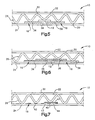
- Figs. 5-7 show several different antenna 18 and processor 12 configurations, where the antenna 18 is positioned directly on the surface of the linerboard 22, 24, rather than on an inlet 14 or label 16.
- Figs. 5 and 6 show a capacitive antenna system and Fig. 7 shows an inductive antenna system.
- a typical capacitive antenna 18 will utilize two areas or pads 36 of conductive material with a gap 38 positioned between the conductive pads 36.
- the processor 12 is positioned within the gap 38 and is electrically coupled to the conductive pads 36.
- Fig. 5 depicts a corrugated structure 10 where a capacitive antenna is positioned on the second linerboard 24 and a capacitive processor 12 is electrically coupled to the antenna.
- the capacitive processor 12 has two terminals and the capacitive antenna includes two conductive pads 36 separated by a gap 38.
- the processor 12 is positioned over the gap 38 so that one terminal of the processor couples to one conductive pad and the other terminal of the processor couples to the other conductive pad.
- Fig. 6 is similar to Fig.
- interposer 20 coupled between the processor 12 and conductive pads 36.
- the interposer 20 serves as the conduit for establishing an electrical connection between the poles of the pads 36 and the terminals of the processor 12.
- an inlet 14 or label 16 may be utilized to position the processor 12 and antenna 18 on the linerboard 22, 24, instead of applying the components directly to the linerboard 22, 24.
- Fig. 7 shows an inductive antenna system, where a processor 12 and a spiral antenna 40 having individual loops is positioned on the second linerboard surface.
- the processor 12 is shown positioned inside the spiral antenna 40.
- the spiral antenna 40 has two ends or poles, with a first pole directly connected to one of the terminals of the processor 12, and a second pole connected to the other terminal by a bridging connector 42.
- the antenna 40 and processor 12 may alternatively be applied to an inlet 14 or label 16, which may be positioned between the second linerboard 24 and corrugated medium 26, as previously discussed.
- Other types of inductive antennas may also be utilized, as known by those of skill in the art.
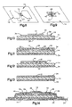
- Figs. 8-12 depict several examples of the inlet 14 and label 16 of the present design.
- the inlet 14 or label 16 may be positioned between the linerboard 22, 24 and corrugated medium 26 of the corrugated structure 10, as previously discussed.
- Figs. 8, 10 and 11 show a capacitive antenna utilizing two conductive pads 36 with a gap 38 positioned between the pads 36.
- a processor 12 is positioned in the gap 38, and is electrically coupled to the conductive pads 36.
- an interposer 20 is positioned between the terminals of the processor 12 and the conductive pads 36. As previously discussed, the interposer 20 serves as the conduit for establishing an electrical connection between the processor 12 and antenna 18.
- Figs. 9 and 12 show an inductive antenna, where the antenna 18 is a spiral loop antenna 40 that is positioned on the inlet surface.
- the processor 12 is positioned in the center of the loop (as shown in cross-section in Fig. 7 ).
- the processor 12 is positioned outside of the loop 40.
- a bridging connector 42 is utilized to connect the outer pole of the antenna 40 to the terminal of the processor 12.
- the inner pole is directly connected to the other terminal of the processor 12.
- An insulating dielectric 44 such as a plastic or nonconductive adhesive, may be positioned between the bridging connector 42 and the antenna loops 40.
- An antenna 18 may be applied to the linerboards 22, 24, corrugated medium 26, or inlet 14 or label 16 by any number of application techniques. With either type of antenna system, the antenna 18 may be formed by depositing metal or other conductive materials, such as by sputter coating, hot foil stamping, or printing a conductive material, such as a polymer or ink, on the substrate. Alternatively, the antenna 18 may be formed by adhesively attaching a preformed antenna 18, or by attaching a preformed antenna 18 on an inlet 14 or label 16. The antenna 18 may be shaped as solid areas of conductive material such as pads 36, or may be formed in more defined shapes, such as a spiral, a coil, a loop, or an arm.
- a conductive area may be formed and the antenna shape may be cut into the conductive area using etching, laser ablation, or mechanical or chemical removal.
- a shaped antenna 18 may be formed by masking off parts of the substrate, depositing a conductive material, and then removing the masking, the invention not being limited to a particular method of forming the antenna 18, or to a particular antenna shape.
- the inlet 14 may be applied to the corrugated medium 26 or linerboards 22, 24 by first applying an adhesive 28 to the corrugated medium 26 or linerboards 22, 24 and then applying the inlet 14 onto the adhesive 28.
- the inlet 14 may also include an adhesive layer 34, as shown in Fig. 13 .
- An adhesive layer 34 may be positioned on either or both the bottom and top of the inlet 14.
- the adhesive may be any type of adhesive.
- the adhesive utilized on the label 16 and inlet 14 may be activated during application of the inlet 14 or label 16 to the corrugated structure 10, such as by water, heat, or pressure.
- Fig. 14 shows an alternative example of the inlet 14 where a backing paper or other substrate 46 is attached to the inlet 14 to form a label 16.
- the backing paper 46 is preferably positioned over the processor on the inlet so that the adhesive 32 layer on the backing paper adheres to the inlet.
- the inlet 14 may also include an adhesive layer 34 that mates with the adhesive layer 32 on the backing paper 46 to adhere the inlet 14 to the backing paper 46.
- the backing paper 46 is preferably larger than the inlet 14 so that a portion of the backing paper 46 extends past the outer edges of the inlet to create a label 16.
- the layer of adhesive 32 on the backing paper 46 also preferably extends past the edges of the inlet 14 so that the label 16 may be attached to a surface.
- the inlet 14 also is shown as including an adhesive layer 34 so that the adhesive 34 of the inlet 14 and the adhesive 32 of the label 16 work in concert to adhere the label to a substrate.
- a paper label 16 may be preferred with certain types of adhesive, such as starch-based glues, rather than a plastic inlet layer so that the label may be more easily adhered to the flutes of the corrugated medium 26.
- a capacitive antenna and processor 12 are shown (for illustration purposes) positioned on top of the inlet 14 in Fig. 14 .
- the corrugated structure described in the various embodiments above may also include an additional sheet (not shown) that is laminated or otherwise adhered to one or more of the linerboards 20, 22, 24.
- the additional sheet can be used for applying a printed surface, such as an exterior, to the corrugated structure, for extra thickness or toughness, or for otherwise altering the appearance of the corrugated structure, among other uses.
- One type of additional sheet is known as a Litholam, which is a lithographically printed sheet that is laminated to one of the linerboards of the corrugated structure. The Litholam sheet is preprinted and then adhered to one of more of the linerboards of the corrugated structure.
- the Litholam is used to provide a high quality printed surface to the corrugated structure, since it is oftentimes difficult to obtain high quality printed corrugated structures by directly printing on the corrugated structure itself.
- the Litholams can be of various colors and include any variety of printing.
- Figs. 15 and 16 depict an assembly line 50 for manufacturing a corrugated structure 10 that includes RFID components.
- the assembly line 50 preferably includes a supply of a first linerboard 22, a supply of a second liner board 24, a supply of a corrugating material stock 48, and a supply 57 of inlets 14, labels 16, or processors 12.
- these inlets, labels, and processors will collectively be referred to as inlets for the assembly line description.
- the inlets 14 may include solely a processor 12, or a processor 12 and antenna 18. When the inlet 14 includes only a processor 12, the processor 12 may include an onboard antenna, or a separate antenna 18 may be positioned on either the corrugated medium 26 or the second linerboard 24.
- the inlets 14 may be supplied in a roll 57, in a fan fold, or already cut into single pieces.
- the assembly line 50 also includes a corrugator 52, a single facer 54, a double facer 56, an inlet applicator 58, and a cutter 60. Numerous idler rollers 62 are also provided.
- the corrugating material stock 48 is fed into the corrugator 52, which corrugates the corrugating material stock 48 into a corrugated medium 26.
- the corrugator 52 is positioned downstream from the supply of corrugating material stock 48.
- An adhesive 28 is applied to the flutes 31 of the corrugated medium 26 by an adhesive applicator 74 after the corrugating material stock 48 is corrugated.
- the first linerboard travel through a preheater 64 and the corrugated medium 26 is then joined to the first linerboard 22 by a single facer 54.
- the second linerboard 24 is fed through a preheater 64, and is then joined to the corrugated medium 26 and first linerboard 22 at the double facer 56.
- an adhesive 28 is applied to the flutes of the corrugated medium 26 by another adhesive applicator 74.
- This adhesive 28 joins the second linerboard 24 to the corrugated medium 26 in the double facer 56.
- the corrugated structure 10 is then fed into a dryer 66, which dries the adhesive 28 and forms the final corrugated structure 10.
- the corrugated structure 10 is then cut by a cutter 60 to form a plurality of blanks 76.
- the RF components may be inserted into the corrugated structure 10 along the assembly process at any number of positions and by any number of ways, as previously discussed.
- An inlet applicator 58 is used to insert an inlet 14 into the structure 10.
- the applicator 58 applies the inlet 14 upstream from the preheater 64.
- the RF processor 12 is preferably capable of withstanding the heat of the preheater 64.
- the applicator 58 is shown positioned downstream from the preheater 64, but upstream from the double facer 56.
- Fig. 16 also shows several other locations where the inlets 14 may be applied to the corrugated structure, labeled by arrows A, B, C, and D.
- Arrow A shows a position for the inlet applicator on the single facer 54 before the corrugated medium is joined to the first linerboard.
- Arrows B and C show a position for the inlet applicator that is downstream from the corrugator, but upstream from the single facer. In this embodiment in accordance with the processor 12 is positioned between the flutes 31 of the corrugated medium 26, in order to avoid crushing the processor between the teeth of one of the single facer rolls.
- Arrow D shows the inlet applicator positioned on the double facer upstream of where the double facer joins the corrugated medium and first linerboard to the second linerboard.
- the inlet 14 may be slid between the rollers of the double facer 56. As discussed above, the inlet 14 may include an adhesive layer 34, if desired.
- the assembly line 50 also includes a registration mechanism 68 for registering the corrugated structure 10 so that a single RF processor 12 is positioned on each blank 76.
- a sensor such as an electric eye
- the sensor senses the preprinted mark and sends a signal to the cutter 60 to cut a blank 76.
- the signal can also be sent to the applicator 58 along a control loop 78, which can signal the applicator 58 to apply an inlet 14 to the structure 10 at an instructed time.
- Other registration techniques may also be utilized, such as one in which the cutter 60 is signaled to cut based upon a length of the blank 76.
- the applicator movement may be triggered by the knife movement. More than one sensor may also be utilized.
- a computer (not shown) may also be utilized along the control loop 78.
- the processor 12 itself may be utilized in registering the moving web of corrugated structure 10.
- a reader may determine the position of the processor 12 on the web. Based upon the sensed position of the processor 12, an operating system will instruct the cutter 60 to cut at a given time, and the applicator 58 to apply an inlet 14 at a given time.
- Other registration techniques may also be utilized as known by those of skill in the art of registering to a moving web.
- a recess may be formed in the substrate on which the processor 12 and antenna 18 are positioned.
- the linerboard 22, 24 may be embossed so that a recess is formed for positioning the processor 12 and antenna 18 in the recess.
- the corrugated medium 26 may be selectively embossed so that the inlet 14 seats within the corrugated medium 26.
- the linerboards 22, 24 or corrugated medium 26 are preferably embossed so that the embossed region is not visible from the exterior of the corrugated structure 10. This is preferred in order to maintain the covert nature of the processor 12 and antenna 18 within the corrugated structure 10.
- the RF processor is passive. However, a semi-passive or active system is also contemplated for use with the present design. If a semi-passive or active processor is utilized, a battery is coupled to the processor.
- a sensor may be electrically coupled to the RF processor for communication with the processor 12, such as a MEMS (micro electromechanical system) sensor. The sensor may be used to read an environmental or other conditions in the vicinity of the sensor, such as time, temperature, pressure, and humidity, among other conditions. Multiple sensors may be utilized with a single or multiple RF processors. The sensors may be utilized to read and transmit a signal corresponding to the environmental or other conditions when signaled by an RF reader.
- MEMS micro electromechanical system
- the sensors may include a battery which allows the sensor to read and record the condition and the recorded data may be transmitted when activated by an RF reader.
- a passive sensor that may be utilized, for example, to read a temperature is manufactured by SCS of San Diego, California.
- a type of active sensor that may be utilized, for example, to record temperature data is manufactured by KSW of Germany.
- Other types of sensors may also be utilized.
- processors are contemplated for use with the claimed invention, including both capacitive processors and inductive processors.
- Some commercially available processors include those manufactured by Phillips, Hitachi and Texas Instruments, among others.
- Conductive leads, traces, or other conducting elements may be utilized, as discussed above, to establish an electrical connection between the processor terminals, and the antenna 18. These leads may be any type of conductive material known to those of skill in the art, such as conductive adhesive, a conductive polymer, or a solder. The leads may be preformed, or may be applied to the processor 12 and/or antenna 18 during the manufacturing process.
- corrugated structures 10, inlets 14, and labels 16 having certain layer thicknesses are shown in the figures, it should be noted that the various relative thicknesses are for illustration purposes only. The actual corrugated structure and RFID components may vary from the sizes and relative dimensions shown in the figures.
Landscapes
- Engineering & Computer Science (AREA)
- Computer Hardware Design (AREA)
- Microelectronics & Electronic Packaging (AREA)
- Physics & Mathematics (AREA)
- General Physics & Mathematics (AREA)
- Theoretical Computer Science (AREA)
- Mechanical Engineering (AREA)
- Machines For Manufacturing Corrugated Board In Mechanical Paper-Making Processes (AREA)
- Details Of Aerials (AREA)
- Laminated Bodies (AREA)
- Internal Circuitry In Semiconductor Integrated Circuit Devices (AREA)
- Control Of Motors That Do Not Use Commutators (AREA)
- Electroluminescent Light Sources (AREA)
Claims (5)
- Eine gewellte Struktur (10), die folgendes umfasst:ein Deckenpapier (22, 24);ein gewelltes Medium (26), das mit dem Deckenpapier (22, 24) gekoppelt ist;einen HF-Prozessor (12), der zwischen das Deckenpapier (22, 24) und dem gewellten Medium (26) gekoppelt ist;
die ferner eine Antenne (18) umfasst, und
das gewellte Medium (26) eine Vielzahl von Rillen (31) aufweist; dadurch gekennzeichnet, dass die Antenne (18) in den HF-Prozessor (12) integriert ist; und der HF-Prozessor (12) zwischen den Rillen (31) des gewellten Mediums (26) positioniert ist. - Die gewellte Struktur nach Anspruch 1, wobei das Deckenpapier ein erstes und ein zweites Deckenpapier umfasst und das gewellte Medium zwischen dem ersten und zweiten Deckenpapier gekoppelt ist, insbesondere
wobei ein Klebstoff zwischen dem ersten und zweiten Deckenpapier und dem gewellten Medium positioniert ist, oder insbesondere
die ferner ein zweites gewelltes Medium und ein drittes Deckenpapier umfasst, wobei das zweite gewellte Medium zwischen dem ersten und dritten Deckenpapier gekoppelt ist, insbesondere
wobei der HF-Prozessor zwischen dem zweiten Deckenpapier und dem gewellten Medium positioniert ist, oder insbesondere
wobei der HF-Prozessor zwischen dem zweiten Deckenpapier und dem gewellten Medium positioniert ist; oder
wobei der HF-Prozessor auf einem Etikett positioniert ist, das einen an einer Seite davon angebrachten Klebstoff aufweist, wobei die Klebstoffseite des Etiketts an dem Deckenpapier angebracht ist, insbesondere
wobei das gewellte Medium eine Vielzahl von Rillen umfasst und ein Klebstoff an den Spitzen der Rillen positioniert ist; oder
wobei der HF-Prozessor an einem Inlet positioniert ist, das einen an einer Seite davon angebrachten Klebstoff aufweist, wobei der Klebstoff des Inlets an dem Deckenpapier angebracht ist, insbesondere
wobei ein Klebstoff an beide Seiten des Inlets gekoppelt ist, wobei eine Seite des Inlets an das gewellte Medium geklebt ist und die andere Seite des Inlets an das Deckenpapier geklebt ist; oder
wobei das gewellte Medium eine Vielzahl von Rillen umfasst und der HF-Prozessor ein Computerchip ist, wobei der Computerchip zwischen zwei aus der Vielzahl von Rillen des gewellten Mediums positioniert ist. - Die gewellte Struktur nach Anspruch 1, die ferner einen Sensor umfasst, der elektrisch mit dem HF-Prozessor gekoppelt und zwischen dem Deckenpapier und dem gewellten Medium positioniert ist, insbesondere
wobei der Sensor ein HF-Sensor eines mikroelektromechanischen Systems ist, oder insbesondere
wobei der Sensor ein Temperatur-, Druck- oder Feuchtigkeitssensor ist; oder
die ferner mindestens einen Materialbogen umfasst, der an dem Deckenpapier befestigt ist. - Ein Verfahren zur Herstellung einer gewellten Struktur (10), die einen eingebetteten HFID-Prozessor aufweist, das folgendes umfasst:Bereitstellen eines Deckenpapiers (22, 24);Bereitstellen eines gewellten Mediums (26);Positionieren eines HF-Prozessors (12) zwischen dem Deckenpapier (22, 24) und dem gewellten Medium (26); undBefestigen des Deckenpapiers (22, 24) und des gewellten Mediums (26) zusammen mit dem HF-Prozessor (12), der zwischen dem Deckenpapier (22, 24) und dem gewellten Medium (26) positioniert ist, zur Herstellung einer gewellten Struktur (10);
wobei
das gewellte Medium (26) eine Vielzahl von Rillen (31) aufweist; dadurch gekennzeichnet, dass eine Antenne (18) in den HF-Prozessor (12) integriert ist; und der HF-Prozessor (12) zwischen den Rillen (31) des gewellten Mediums (26) positioniert ist. - Das Verfahren nach Anspruch 4, das ferner das Positionieren des HF-Prozessors auf einem Inlet umfasst, das einen an einer Seite davon angebrachten Klebstoff aufweist, und wobei der Positionierungsschritt das Aufbringen der Klebstoffseite des Inlets auf eines aus dem Deckenpapier oder dem gewellten Medium einschließt, insbesondere
das ferner das Aufkleben des Inlets auf ein Etikett umfasst, das einen an einer Seite davon angebrachten Klebstoff aufweist, und wobei der Positionierungsschritt das Aufbringen der Klebstoffseite des Etiketts und der Klebstoffseite des Inlets auf eines aus dem Deckenpapier oder dem gewellten Medium einschließt; oder
wobei der HF-Prozessor einen Computerchip umfasst und das gewellte Medium eine Vielzahl von Rillen einschließt, und der Positionierungsschritt das Positionieren des HF-Chips zwischen zwei aus der Vielzahl von Rillen einschließt; oder
wobei das Deckenpapier ein erstes und ein zweites Deckenpapier umfasst und der Befestigungsschritt das Einklemmen des gewellten Mediums zwischen dem ersten und zweiten Deckenpapier einschließt, insbesondere
wobei der Positionierungsschritt das Positionieren des HF-Prozessors zwischen dem zweiten Deckenpapier und dem gewellten Medium einschließt; oder
das ferner das Aufbringen eines Klebstoffs an eines aus dem Deckenpapier oder dem gewellten Medium umfasst; oder
das ferner das Schneiden der gewellten Struktur mit einem Schneidegerät zu einer Vielzahl von Zuschnitten umfasst, insbesondere
das ferner das Registrieren des Schneideschritts mit dem Positionierungsschritt umfasst, so dass ein einziger HF-Prozessor mit jedem Zuschnitt gekoppelt wird, insbesondere
wobei der Registrierungsschritt das Lesen des HF-Prozessors unter Verwendung eines HFID-Lesegeräts zur Erkennung der Position des Prozessors einschließt, und das ferner das Koordinieren der erkannten Position des Prozessors mit dem Schneidegerät umfasst, um jeden gewellten Zuschnitt zu schneiden, oder insbesondere
wobei die gewellte Struktur eine Registriermarkierung einschließt, die von einer Registriervorrichtung gelesen werden kann, und wobei der Registrierungsschritt das Lesen einer Position der Registriermarkierung und das Korrelieren des Lesens der Registriermarkierung mit dem Positionieren des HF-Prozessors und dem Schneiden der gewellten Struktur einschließt, insbesondere
wobei der Prozessor eine integrierte Antenne aufweist, und das ferner das Koppeln des Prozessors mit einem Inlet umfasst und der Positionierungsschritt das Positionieren des Inlets zwischen dem Deckenpapier und dem gewellten Medium einschließt, insbesondere
das ferner das Koppeln des Inlets mit einem Etikett umfasst, wobei der Positionierungsschritt das Positionieren des Etiketts zwischen dem Deckenpapier und dem gewellten Medium einschließt; oder
das ferner folgendes umfasst:Bereitstellen eines Inlets; undBefestigen des HF-Prozessors an dem Inlet, wobei der Positionierungsschritt das Positionieren des Inlets mit dem HF-Prozessor zwischen dem Deckenpapier und dem gewellten Medium umfasst; oderdas ferner das elektrische Koppeln eines Sensors mit dem HF-Prozessor zwischen dem Deckenpapier und dem gewellten Medium umfasst.
Applications Claiming Priority (3)
| Application Number | Priority Date | Filing Date | Title |
|---|---|---|---|
| US10/256,940 US6667092B1 (en) | 2002-09-26 | 2002-09-26 | RFID enabled corrugated structures |
| US256940 | 2002-09-26 | ||
| PCT/IB2003/004137 WO2004029872A1 (en) | 2002-09-26 | 2003-09-24 | Rfid enabled corrugated structures |
Publications (2)
| Publication Number | Publication Date |
|---|---|
| EP1550078A1 EP1550078A1 (de) | 2005-07-06 |
| EP1550078B1 true EP1550078B1 (de) | 2010-06-30 |
Family
ID=29735631
Family Applications (1)
| Application Number | Title | Priority Date | Filing Date |
|---|---|---|---|
| EP03798322A Revoked EP1550078B1 (de) | 2002-09-26 | 2003-09-24 | Rfid-fähige gerillte strukturen |
Country Status (13)
| Country | Link |
|---|---|
| US (1) | US6667092B1 (de) |
| EP (1) | EP1550078B1 (de) |
| CN (1) | CN1703716A (de) |
| AT (1) | ATE472777T1 (de) |
| AU (1) | AU2003263470A1 (de) |
| BR (1) | BR0314731A (de) |
| CA (1) | CA2500273A1 (de) |
| DE (1) | DE60333209D1 (de) |
| ES (1) | ES2345251T3 (de) |
| MX (1) | MXPA05004329A (de) |
| RU (1) | RU2005112448A (de) |
| TW (1) | TWI273975B (de) |
| WO (1) | WO2004029872A1 (de) |
Cited By (2)
| Publication number | Priority date | Publication date | Assignee | Title |
|---|---|---|---|---|
| DE102008019938B4 (de) | 2007-05-04 | 2022-09-22 | Heidelberger Druckmaschinen Ag | Anordnung zum Detektieren einer physikalischen Größe an einem Stapel aufeinander liegender Bogen |
| WO2026015798A1 (en) * | 2024-07-12 | 2026-01-15 | Sojo Industries, Inc. | Cargo tracking device, system, and method |
Families Citing this family (109)
| Publication number | Priority date | Publication date | Assignee | Title |
|---|---|---|---|---|
| US7204652B2 (en) * | 1999-06-16 | 2007-04-17 | Vanguard Identification Systems, Inc. | Printed planar radio frequency identification elements |
| US8077040B2 (en) | 2000-01-24 | 2011-12-13 | Nextreme, Llc | RF-enabled pallet |
| US6943678B2 (en) | 2000-01-24 | 2005-09-13 | Nextreme, L.L.C. | Thermoformed apparatus having a communications device |
| US7342496B2 (en) * | 2000-01-24 | 2008-03-11 | Nextreme Llc | RF-enabled pallet |
| US7224280B2 (en) * | 2002-12-31 | 2007-05-29 | Avery Dennison Corporation | RFID device and method of forming |
| FI116318B (fi) * | 2003-02-27 | 2005-10-31 | Avantone Oy | Painetut TTI-indikaattorit |
| US7055754B2 (en) * | 2003-11-03 | 2006-06-06 | Avery Dennison Corporation | Self-compensating antennas for substrates having differing dielectric constant values |
| US6914562B2 (en) * | 2003-04-10 | 2005-07-05 | Avery Dennison Corporation | RFID tag using a surface insensitive antenna structure |
| US7501984B2 (en) | 2003-11-04 | 2009-03-10 | Avery Dennison Corporation | RFID tag using a surface insensitive antenna structure |
| US7652636B2 (en) | 2003-04-10 | 2010-01-26 | Avery Dennison Corporation | RFID devices having self-compensating antennas and conductive shields |
| CA2430242A1 (en) * | 2003-06-06 | 2004-12-06 | Kimihiko Ernst Sato | Large array of radio frequency id transponders deployed in an array by use of deploying rows of transponders that unwind from long spools of high strength fiber or tape with passive rfid transponders separated by fixed lengths |
| DE10331509B3 (de) * | 2003-07-11 | 2004-12-23 | Infineon Technologies Ag | Verfahren und eine Vorrichtung zur Herstellung eines Flächengebildes |
| WO2005035258A2 (en) * | 2003-10-07 | 2005-04-21 | Rock-Tenn Company | Packaging material with embedded security mechanisms |
| US20050269819A1 (en) * | 2003-10-07 | 2005-12-08 | Chambers James D | Packaging with embedded security measures |
| US7370808B2 (en) * | 2004-01-12 | 2008-05-13 | Symbol Technologies, Inc. | Method and system for manufacturing radio frequency identification tag antennas |
| AU2005208313A1 (en) * | 2004-01-22 | 2005-08-11 | Mikoh Corporation | A modular radio frequency identification tagging method |
| US7036734B2 (en) * | 2004-02-04 | 2006-05-02 | Venture Research Inc. | Free standing column-shaped structure for housing RFID antennas and readers |
| JP4567988B2 (ja) * | 2004-02-05 | 2010-10-27 | 株式会社日立製作所 | 紙状rfidタグおよびその製造方法 |
| US7704346B2 (en) | 2004-02-23 | 2010-04-27 | Checkpoint Systems, Inc. | Method of fabricating a security tag in an integrated surface processing system |
| US7384496B2 (en) | 2004-02-23 | 2008-06-10 | Checkpoint Systems, Inc. | Security tag system for fabricating a tag including an integrated surface processing system |
| JP2005306470A (ja) * | 2004-03-25 | 2005-11-04 | Tatsuo Sasazaki | シート状成形材 |
| US7102518B2 (en) * | 2004-04-05 | 2006-09-05 | Sonoco Development, Inc. | Removable identification device for multilayer tubular structures |
| ITMO20040080A1 (it) * | 2004-04-08 | 2004-07-08 | Windinglab S R L | Metodo di realizzazione di un circuito stampato di spessore sottile e circuito relativo |
| US7183998B2 (en) * | 2004-06-02 | 2007-02-27 | Sciperio, Inc. | Micro-helix antenna and methods for making same |
| US7088229B2 (en) * | 2004-06-14 | 2006-08-08 | Oracle International Corporation | Methods and systems for verifying the position and status of hierarchically arranged objects |
| US7292148B2 (en) * | 2004-06-18 | 2007-11-06 | Avery Dennison Corporation | Method of variable position strap mounting for RFID transponder |
| WO2006009140A1 (ja) * | 2004-07-20 | 2006-01-26 | Dai Nippon Printing Co., Ltd. | 無線icタグ付き包装体 |
| FR2874442B1 (fr) * | 2004-08-20 | 2007-06-29 | Kaysersberg Packaging Soc Par | Procede pour appliquer des transpondeurs d'identification par radiofrequence sur des feuilles d'emballage, support de transpondeurs |
| US7253736B2 (en) * | 2004-08-26 | 2007-08-07 | Sdgi Holdings, Inc. | RFID tag for instrument handles |
| ES2303035T3 (es) * | 2004-09-06 | 2008-08-01 | Upm Raflatac Oy | Una etiqueta que comprende un transpondedor y un sistema que comprende un transpondedor. |
| US20060054705A1 (en) * | 2004-09-08 | 2006-03-16 | Georgia-Pacific Corporation | Package insert with integrated radio frequency transponder |
| US7501955B2 (en) | 2004-09-13 | 2009-03-10 | Avery Dennison Corporation | RFID device with content insensitivity and position insensitivity |
| WO2006031824A2 (en) * | 2004-09-14 | 2006-03-23 | Adasa, Inc. | Systems and methods for deployment and recycling of rfid tags, wireless sensors, and the containers attached thereto |
| US20060125642A1 (en) * | 2004-12-02 | 2006-06-15 | Chandaria Ashok V | Container with internal radio frequency identification tag |
| US7209042B2 (en) * | 2004-12-20 | 2007-04-24 | Temptime Corporation | RFID tag with visual environmental condition monitor |
| JP4871140B2 (ja) * | 2004-12-27 | 2012-02-08 | 王子製紙株式会社 | 感熱記録多重シート及びその製造方法 |
| DE102005032014B4 (de) * | 2005-04-19 | 2009-03-12 | Helmut Holl | Verfahren zum Herstellen einer Verpackung aus Wellpappe und Vorrichtung |
| EP1715447A3 (de) * | 2005-04-20 | 2009-05-06 | Heinrich Karl Peppler | Verfahren und Vorrichtung zur elektronischer Kennzeichnung von Verpackungen sowie Verpackung |
| US9114187B2 (en) * | 2005-04-28 | 2015-08-25 | Zih Corp. | Antimicrobial coating for identification devices |
| US7466233B2 (en) * | 2005-05-04 | 2008-12-16 | Adalis Corporation | Substrates including tape and radio frequency identification devices, and methods and apparatus for making the same |
| US7477150B2 (en) * | 2005-05-04 | 2009-01-13 | Adalis Corporation | Radio frequency identification tag reinforcing tape and methods |
| WO2006119279A2 (en) * | 2005-05-04 | 2006-11-09 | Adalis Corporation | Radio frequency identification tag reinforcing tape, substrates including tape, and methods and apparatus for making the same |
| US20060290511A1 (en) * | 2005-06-22 | 2006-12-28 | Kenneth Shanton | Methods and systems for in-line RFID transponder assembly |
| US20060290512A1 (en) * | 2005-06-22 | 2006-12-28 | Smurfit-Stone Container Enterprises, Inc. | Methods and apparatus for RFID transponder fabrication |
| US7651032B2 (en) * | 2005-06-22 | 2010-01-26 | Smurfit-Stone Container Enterprises, Inc. | Methods and systems for in-line RFID transponder assembly |
| US20070052521A1 (en) * | 2005-09-02 | 2007-03-08 | Micro Trak Gps, Inc. | Mounting apparatus for radio frequency identification system |
| WO2007034518A1 (en) * | 2005-09-22 | 2007-03-29 | Serfina S.R.L. | Packaging material with radiofrequency tag |
| TW200713074A (en) * | 2005-09-26 | 2007-04-01 | Ind Tech Res Inst | Flexible RFID label and manufacturing method thereof |
| US20070075125A1 (en) * | 2005-09-30 | 2007-04-05 | Muscat Robert G | Packaging and process of authenticating packaging |
| US20080022098A1 (en) * | 2005-09-30 | 2008-01-24 | Muscat Robert G | Authentication process |
| US20070080804A1 (en) * | 2005-10-07 | 2007-04-12 | Edwin Hirahara | Systems and methods for enhanced RFID tag performance |
| US8067253B2 (en) | 2005-12-21 | 2011-11-29 | Avery Dennison Corporation | Electrical device and method of manufacturing electrical devices using film embossing techniques to embed integrated circuits into film |
| US7605708B2 (en) * | 2005-12-22 | 2009-10-20 | Checkpoint Systems, Inc. | Smart corrugated cardboard |
| US7579951B2 (en) * | 2005-12-28 | 2009-08-25 | Organicid, Inc | Tracking radio frequency identification tags |
| US7388506B2 (en) | 2006-02-07 | 2008-06-17 | Rexam Healthcare Packaging Inc. | Closure and package with induction seal and RFID tag |
| DE102006007290B3 (de) * | 2006-02-16 | 2007-11-22 | Texmag Gmbh Vertriebsgesellschaft Gmbh | Verfahren zur Einbringung von RFID-Tags in Wellpappe und Materialstück aus Pappe mit RFID-Tag |
| US20070279230A1 (en) * | 2006-06-01 | 2007-12-06 | Wavezero, Inc. | System and Method for Attaching Radiofrequency Identification Chips to Metalized Antenna |
| WO2008060708A2 (en) * | 2006-06-09 | 2008-05-22 | Arjobex America | Laminate device having voided structure for carrying electronic element, such as label for rfid tag |
| US7887755B2 (en) * | 2006-09-20 | 2011-02-15 | Binforma Group Limited Liability Company | Packaging closures integrated with disposable RFID devices |
| US20080179404A1 (en) * | 2006-09-26 | 2008-07-31 | Advanced Microelectronic And Automation Technology Ltd. | Methods and apparatuses to produce inlays with transponders |
| US8608080B2 (en) | 2006-09-26 | 2013-12-17 | Feinics Amatech Teoranta | Inlays for security documents |
| US8322624B2 (en) * | 2007-04-10 | 2012-12-04 | Feinics Amatech Teoranta | Smart card with switchable matching antenna |
| US7581308B2 (en) | 2007-01-01 | 2009-09-01 | Advanced Microelectronic And Automation Technology Ltd. | Methods of connecting an antenna to a transponder chip |
| US8240022B2 (en) * | 2006-09-26 | 2012-08-14 | Feinics Amatech Teorowita | Methods of connecting an antenna to a transponder chip |
| US7979975B2 (en) * | 2007-04-10 | 2011-07-19 | Feinics Amatech Teavanta | Methods of connecting an antenna to a transponder chip |
| US7546671B2 (en) * | 2006-09-26 | 2009-06-16 | Micromechanic And Automation Technology Ltd. | Method of forming an inlay substrate having an antenna wire |
| EP1939794A3 (de) | 2006-12-29 | 2009-04-01 | Vanguard Identification Systems, Inc. | Gedruckte, flache Armbänder mit RFID-Elementen und ähnliche persönliche Identifikationsvorrichtungen |
| WO2008096574A1 (ja) * | 2007-02-06 | 2008-08-14 | Murata Manufacturing Co., Ltd. | 電磁結合モジュール付き包装材 |
| WO2008096576A1 (ja) * | 2007-02-06 | 2008-08-14 | Murata Manufacturing Co., Ltd. | 電磁結合モジュール付き包装材 |
| US20080191001A1 (en) * | 2007-02-08 | 2008-08-14 | Kapoor Chandaria | Packaging having protective materials incorporated therein |
| US20080190790A1 (en) * | 2007-02-08 | 2008-08-14 | Kitaru Innovations Inc. | Storage box having protective materials incorporated therein |
| DE102007008303A1 (de) * | 2007-02-16 | 2008-08-21 | Paschal-Werk G. Maier Gmbh | Schalungselement mit Identifizierungsmittel |
| EP1972565A1 (de) | 2007-03-19 | 2008-09-24 | Mondi Technology Investments SA | Verpackung |
| US7980477B2 (en) * | 2007-05-17 | 2011-07-19 | Féinics Amatech Teoranta | Dual interface inlays |
| FR2918485B1 (fr) * | 2007-07-04 | 2010-09-10 | Arjowiggins Licensing Sas | Support fibreux pour insert comportant une antenne |
| TW200904733A (en) * | 2007-07-26 | 2009-02-01 | Yfy Rfid Technologies Company Ltd | Radio frequency identification tag holder and paper roll assembly |
| US7855648B2 (en) | 2007-08-14 | 2010-12-21 | Avery Dennison Corporation | RFID tag |
| KR100905295B1 (ko) | 2007-10-09 | 2009-07-16 | 주식회사 삼보판지 | 골판지용 rfid 탑재장치 |
| KR100933089B1 (ko) * | 2007-10-10 | 2009-12-22 | 주식회사 삼보판지 | 골판지용 rfid 탑재장치 |
| KR100931960B1 (ko) * | 2007-10-10 | 2009-12-15 | 주식회사 삼보판지 | 박스용 골판지와 그 제조방법 |
| EP2071496A1 (de) * | 2007-12-13 | 2009-06-17 | Mondi AG | Verfahren zur Herstellung einer flexiblen Verpackung mit RFID Transponder |
| US20100001837A1 (en) * | 2008-07-07 | 2010-01-07 | Mazzella Lifting Technologies | Attachable rfid devices and methods for identifying objects |
| KR20100098272A (ko) * | 2009-02-27 | 2010-09-06 | 이봉수 | 전자태그를 갖는 포장상자 |
| US8910854B2 (en) * | 2009-03-11 | 2014-12-16 | Packaging Corporation Of America | Container having reinforcing linerboard and methods of making the same |
| US8228260B2 (en) * | 2009-05-08 | 2012-07-24 | Sonoco Development, Inc. | Structure having an antenna incorporated therein |
| US20100323867A1 (en) * | 2009-06-19 | 2010-12-23 | Jian Tao | Method of Making Paper Packing Box |
| KR101131111B1 (ko) * | 2010-02-26 | 2012-04-03 | 류용승 | 골판지를 이용한 rfid 탑재 박스의 제조방법 |
| KR101131104B1 (ko) * | 2010-02-26 | 2012-04-03 | 류용승 | 골판지를 이용한 rfid 탑재 박스의 제조방법 |
| KR101131106B1 (ko) * | 2010-02-26 | 2012-04-03 | 류용승 | 골판지를 이용한 rfid 탑재 박스의 제조방법 |
| US8701271B2 (en) * | 2010-04-14 | 2014-04-22 | Avery Dennison Corporation | Method of assembly of articles |
| US20110315567A1 (en) * | 2010-06-29 | 2011-12-29 | Clever Girl Concepts, LLC | Customizable Storage Container System |
| IT1401198B1 (it) * | 2010-07-14 | 2013-07-12 | Prima S P A | Metodo di produzione di involucri per imballaggio alimentare dotati di dispositivo antifurto del tipo eas, linea di produzione per l'esecuzione del metodo e involucri cosi' ottenuti. |
| FI124073B (fi) * | 2010-09-17 | 2014-03-14 | Stora Enso Oyj | Älypakkaus |
| US9119285B2 (en) | 2012-06-19 | 2015-08-25 | Apple Inc. | Conductive gaskets with internal cavities |
| US9072165B2 (en) | 2012-06-19 | 2015-06-30 | Apple Inc. | Hollow conductive gaskets with curves and openings |
| US9841494B2 (en) * | 2015-01-05 | 2017-12-12 | Locatorx, Inc. | Global resource locator |
| WO2016113596A1 (en) * | 2015-01-14 | 2016-07-21 | Alzumaya Ayoub | Indicator for the quality of a product |
| WO2016206063A1 (zh) * | 2015-06-26 | 2016-12-29 | 田艺儿 | 一种具有rfid射频读写功能的瓦楞纸板的制造方法 |
| CN204802204U (zh) * | 2015-06-26 | 2015-11-25 | 深圳市骄冠科技实业有限公司 | 一种具有rfid射频读写功能的瓦楞纸箱 |
| BR112019012977A8 (pt) * | 2016-12-29 | 2023-02-28 | Avery Dennison Retail Information Services Llc | Cinta de dupla função para elementos ressonantes e antenas de alta frequência |
| KR102440191B1 (ko) | 2017-04-05 | 2022-09-05 | 라이텐, 인코포레이티드 | 주파수 선택 요소를 갖는 안테나 |
| DE102017122052A1 (de) * | 2017-09-22 | 2019-03-28 | Schreiner Group Gmbh & Co. Kg | RFID-Etikett mit Schutz der RFID-Funktion |
| CN112585612B (zh) | 2018-08-09 | 2021-12-24 | 利腾股份有限公司 | 电磁状态感测装置 |
| US11446966B2 (en) | 2019-03-27 | 2022-09-20 | Lyten, Inc. | Tires containing resonating carbon-based microstructures |
| US11479062B2 (en) | 2019-03-27 | 2022-10-25 | Lyten, Inc. | Tuned radio frequency (RF) resonant materials and material configurations for sensing in a vehicle |
| JP7467990B2 (ja) * | 2020-03-04 | 2024-04-16 | 大日本印刷株式会社 | Rfタグ付き段ボールおよびrfタグ付き段ボールの製造方法 |
| DE202021101432U1 (de) * | 2021-03-22 | 2022-06-23 | Tiger Media Deutschland Gmbh | Funktionsgegenstand mit einem Transponder und System mit einem solchen Funktionsgegenstand |
| IT202100030563A1 (it) * | 2021-12-02 | 2023-06-02 | Quantumcorrugated S R L | Impianto di produzione di cartone ondulato con doppio lato di uscita |
| CN114792123B (zh) * | 2022-05-06 | 2025-02-07 | 河南旺鑫食品有限公司 | 用于追溯空心贡面生产制造信息的挂面束 |
Family Cites Families (37)
| Publication number | Priority date | Publication date | Assignee | Title |
|---|---|---|---|---|
| NO126975B (de) | 1967-03-30 | 1973-04-16 | John Welsh | |
| US3707711A (en) | 1970-04-02 | 1972-12-26 | Peter Harold Cole | Electronic surveillance system |
| GB1481050A (en) | 1973-10-30 | 1977-07-27 | Mitsubishi Petrochemical Co | Corrugated cardboard sheet and method for producing the same |
| US4311746A (en) | 1978-02-15 | 1982-01-19 | Chavannes Marc A | Corrugated paper board |
| US4369082A (en) | 1980-07-08 | 1983-01-18 | The Meyercord Co. | Method and apparatus for applying decals to articles |
| US5103235A (en) | 1988-12-30 | 1992-04-07 | Checkpoint Systems, Inc. | Antenna structure for an electronic article surveillance system |
| US5497140A (en) | 1992-08-12 | 1996-03-05 | Micron Technology, Inc. | Electrically powered postage stamp or mailing or shipping label operative with radio frequency (RF) communication |
| DE4319878A1 (de) | 1992-06-17 | 1993-12-23 | Micron Technology Inc | Hochfrequenz-Identifikationseinrichtung (HFID) und Verfahren zu ihrer Herstellung |
| US5831531A (en) | 1992-07-27 | 1998-11-03 | Micron Communications, Inc. | Anti-theft method for detecting the unauthorized opening of containers and baggage |
| US5406263A (en) | 1992-07-27 | 1995-04-11 | Micron Communications, Inc. | Anti-theft method for detecting the unauthorized opening of containers and baggage |
| US5486405A (en) * | 1992-10-14 | 1996-01-23 | Hans Kolb Wellpappe Gmbh & Co. | Method of producing a corrugated board as well as a corrugated board |
| ZA941671B (en) | 1993-03-11 | 1994-10-12 | Csir | Attaching an electronic circuit to a substrate. |
| US5528222A (en) | 1994-09-09 | 1996-06-18 | International Business Machines Corporation | Radio frequency circuit and memory in thin flexible package |
| US5637377A (en) * | 1995-05-31 | 1997-06-10 | Sunclipse, Inc. | Protective containerboard for electrostatic discharge sensitive devices |
| US5908135A (en) | 1995-11-21 | 1999-06-01 | Bradford Company | Sleeve pack |
| US5871100A (en) | 1995-12-22 | 1999-02-16 | Rayovac Corporation | Security battery package |
| US6027027A (en) | 1996-05-31 | 2000-02-22 | Lucent Technologies Inc. | Luggage tag assembly |
| US5821859A (en) | 1996-06-07 | 1998-10-13 | Ibm Corporation | Concealed magnetic ID code and antitheft tag |
| FR2760225B1 (fr) * | 1997-02-28 | 1999-05-21 | Smurfit Socar Sa | Conditionnement en carton ondule equipe d'un moyen d'enregistrement et d'identification d'informations |
| US5884425A (en) | 1997-05-23 | 1999-03-23 | Avery Dennison Corporation | Anti-tamper tag with theft protection |
| US6025780A (en) | 1997-07-25 | 2000-02-15 | Checkpoint Systems, Inc. | RFID tags which are virtually activated and/or deactivated and apparatus and methods of using same in an electronic security system |
| US5982284A (en) | 1997-09-19 | 1999-11-09 | Avery Dennison Corporation | Tag or label with laminated thin, flat, flexible device |
| US5909176A (en) | 1997-09-23 | 1999-06-01 | Intermec Ip Corporation | Anti-theft and identification devices for concealing in articles |
| FR2772529B1 (fr) * | 1997-12-17 | 2000-02-04 | Smurfit Worldwide Research Eur | Subsrat muni d'un dispositif electronique |
| US6019865A (en) | 1998-01-21 | 2000-02-01 | Moore U.S.A. Inc. | Method of forming labels containing transponders |
| US6278379B1 (en) | 1998-04-02 | 2001-08-21 | Georgia Tech Research Corporation | System, method, and sensors for sensing physical properties |
| US6028518A (en) | 1998-06-04 | 2000-02-22 | Checkpoint Systems, Inc. | System for verifying attachment of an EAS marker to an article after tagging |
| US6091332A (en) | 1998-06-09 | 2000-07-18 | Motorola, Inc. | Radio frequency identification tag having printed circuit interconnections |
| US6246327B1 (en) | 1998-06-09 | 2001-06-12 | Motorola, Inc. | Radio frequency identification tag circuit chip having printed interconnection pads |
| US6130613A (en) | 1998-06-09 | 2000-10-10 | Motorola, Inc. | Radio frequency indentification stamp and radio frequency indentification mailing label |
| US6114962A (en) | 1998-10-15 | 2000-09-05 | Intermec Ip Corp. | RF tag having strain relieved stiff substrate and hydrostatic protection for a chip mounted thereto |
| ATE202428T1 (de) | 1999-01-23 | 2001-07-15 | Ident Gmbh X | Rfid-transponder mit bedruckbarer oberfläche |
| US6259369B1 (en) | 1999-09-30 | 2001-07-10 | Moore North America, Inc. | Low cost long distance RFID reading |
| DE19963300C1 (de) | 1999-12-27 | 2001-03-01 | Smart Tec Gmbh & Co Kg | Transponderetikett mit Schutzbeschichtung |
| US6281795B1 (en) | 2000-02-08 | 2001-08-28 | Moore North America, Inc. | RFID or EAS label mount with double sided tape |
| US6696954B2 (en) | 2000-10-16 | 2004-02-24 | Amerasia International Technology, Inc. | Antenna array for smart RFID tags |
| DE10140286B4 (de) * | 2001-08-16 | 2004-05-06 | Panther Packaging Gmbh & Co. Kg | Verfahren zur Herstellung von mit Transpondern versehener Wellpappe und mit Transpondern versehene Wellpappe |
-
2002
- 2002-09-26 US US10/256,940 patent/US6667092B1/en not_active Expired - Fee Related
-
2003
- 2003-09-19 TW TW092125837A patent/TWI273975B/zh not_active IP Right Cessation
- 2003-09-24 DE DE60333209T patent/DE60333209D1/de not_active Expired - Lifetime
- 2003-09-24 ES ES03798322T patent/ES2345251T3/es not_active Expired - Lifetime
- 2003-09-24 CA CA002500273A patent/CA2500273A1/en not_active Abandoned
- 2003-09-24 MX MXPA05004329A patent/MXPA05004329A/es active IP Right Grant
- 2003-09-24 RU RU2005112448/09A patent/RU2005112448A/ru not_active Application Discontinuation
- 2003-09-24 AU AU2003263470A patent/AU2003263470A1/en not_active Abandoned
- 2003-09-24 WO PCT/IB2003/004137 patent/WO2004029872A1/en not_active Ceased
- 2003-09-24 EP EP03798322A patent/EP1550078B1/de not_active Revoked
- 2003-09-24 AT AT03798322T patent/ATE472777T1/de not_active IP Right Cessation
- 2003-09-24 CN CNA038254123A patent/CN1703716A/zh active Pending
- 2003-09-24 BR BR0314731-2A patent/BR0314731A/pt not_active IP Right Cessation
Cited By (2)
| Publication number | Priority date | Publication date | Assignee | Title |
|---|---|---|---|---|
| DE102008019938B4 (de) | 2007-05-04 | 2022-09-22 | Heidelberger Druckmaschinen Ag | Anordnung zum Detektieren einer physikalischen Größe an einem Stapel aufeinander liegender Bogen |
| WO2026015798A1 (en) * | 2024-07-12 | 2026-01-15 | Sojo Industries, Inc. | Cargo tracking device, system, and method |
Also Published As
| Publication number | Publication date |
|---|---|
| EP1550078A1 (de) | 2005-07-06 |
| CN1703716A (zh) | 2005-11-30 |
| US6667092B1 (en) | 2003-12-23 |
| TWI273975B (en) | 2007-02-21 |
| TW200416135A (en) | 2004-09-01 |
| RU2005112448A (ru) | 2005-11-10 |
| CA2500273A1 (en) | 2004-04-08 |
| WO2004029872A1 (en) | 2004-04-08 |
| AU2003263470A1 (en) | 2004-04-19 |
| ES2345251T3 (es) | 2010-09-20 |
| ATE472777T1 (de) | 2010-07-15 |
| MXPA05004329A (es) | 2005-11-23 |
| DE60333209D1 (de) | 2010-08-12 |
| BR0314731A (pt) | 2005-08-30 |
Similar Documents
| Publication | Publication Date | Title |
|---|---|---|
| EP1550078B1 (de) | Rfid-fähige gerillte strukturen | |
| EP2309589B1 (de) | Rfid-etikett mit einer flächenunempfindlichen antennenstruktur | |
| JP4567988B2 (ja) | 紙状rfidタグおよびその製造方法 | |
| EP1817721B1 (de) | Rfid-marken mit modifizierbaren betriebsparametern | |
| US7501984B2 (en) | RFID tag using a surface insensitive antenna structure | |
| US7363704B2 (en) | RFID tag and method of manufacturing RFID tag | |
| AU2017258964A1 (en) | A modular radio frequency identification tagging method | |
| US20070040028A1 (en) | RFID tag | |
| CN101558417A (zh) | 具有防粘衬里窗口的rfid标签及制造方法 | |
| JP5447515B2 (ja) | 無線icデバイス及びその製造方法 | |
| EP2024910B1 (de) | Verfahren zur herstellung von transponder umfassenden produkten | |
| CN101459273B (zh) | 无线射频识别询答器之天线构造及其制造方法 | |
| US20060290512A1 (en) | Methods and apparatus for RFID transponder fabrication | |
| EP1620916B1 (de) | Hfid-etikett mit einer oberflächenunempfindlichen antennenstruktur | |
| JP5082707B2 (ja) | Icタグ付きラベル及びicタグ付きラベルの使用方法 | |
| EP1804203B1 (de) | RFID-Etikett | |
| JP4882365B2 (ja) | 金属対応の非接触式データキャリア配設部材 | |
| JP2006139326A (ja) | Icタグインレット |
Legal Events
| Date | Code | Title | Description |
|---|---|---|---|
| PUAI | Public reference made under article 153(3) epc to a published international application that has entered the european phase |
Free format text: ORIGINAL CODE: 0009012 |
|
| 17P | Request for examination filed |
Effective date: 20050420 |
|
| AK | Designated contracting states |
Kind code of ref document: A1 Designated state(s): AT BE BG CH CY CZ DE DK EE ES FI FR GB GR HU IE IT LI LU MC NL PT RO SE SI SK TR |
|
| AX | Request for extension of the european patent |
Extension state: AL LT LV MK |
|
| DAX | Request for extension of the european patent (deleted) | ||
| 17Q | First examination report despatched |
Effective date: 20090619 |
|
| GRAP | Despatch of communication of intention to grant a patent |
Free format text: ORIGINAL CODE: EPIDOSNIGR1 |
|
| GRAS | Grant fee paid |
Free format text: ORIGINAL CODE: EPIDOSNIGR3 |
|
| GRAA | (expected) grant |
Free format text: ORIGINAL CODE: 0009210 |
|
| AK | Designated contracting states |
Kind code of ref document: B1 Designated state(s): AT BE BG CH CY CZ DE DK EE ES FI FR GB GR HU IE IT LI LU MC NL PT RO SE SI SK TR |
|
| REG | Reference to a national code |
Ref country code: GB Ref legal event code: FG4D Ref country code: CH Ref legal event code: EP |
|
| REG | Reference to a national code |
Ref country code: IE Ref legal event code: FG4D |
|
| REF | Corresponds to: |
Ref document number: 60333209 Country of ref document: DE Date of ref document: 20100812 Kind code of ref document: P |
|
| REG | Reference to a national code |
Ref country code: ES Ref legal event code: FG2A Ref document number: 2345251 Country of ref document: ES Kind code of ref document: T3 |
|
| REG | Reference to a national code |
Ref country code: NL Ref legal event code: VDEP Effective date: 20100630 |
|
| PG25 | Lapsed in a contracting state [announced via postgrant information from national office to epo] |
Ref country code: SE Free format text: LAPSE BECAUSE OF FAILURE TO SUBMIT A TRANSLATION OF THE DESCRIPTION OR TO PAY THE FEE WITHIN THE PRESCRIBED TIME-LIMIT Effective date: 20100630 |
|
| PGFP | Annual fee paid to national office [announced via postgrant information from national office to epo] |
Ref country code: ES Payment date: 20100927 Year of fee payment: 8 |
|
| PG25 | Lapsed in a contracting state [announced via postgrant information from national office to epo] |
Ref country code: AT Free format text: LAPSE BECAUSE OF FAILURE TO SUBMIT A TRANSLATION OF THE DESCRIPTION OR TO PAY THE FEE WITHIN THE PRESCRIBED TIME-LIMIT Effective date: 20100630 Ref country code: SI Free format text: LAPSE BECAUSE OF FAILURE TO SUBMIT A TRANSLATION OF THE DESCRIPTION OR TO PAY THE FEE WITHIN THE PRESCRIBED TIME-LIMIT Effective date: 20100630 Ref country code: FI Free format text: LAPSE BECAUSE OF FAILURE TO SUBMIT A TRANSLATION OF THE DESCRIPTION OR TO PAY THE FEE WITHIN THE PRESCRIBED TIME-LIMIT Effective date: 20100630 |
|
| PGFP | Annual fee paid to national office [announced via postgrant information from national office to epo] |
Ref country code: FR Payment date: 20100930 Year of fee payment: 8 Ref country code: IT Payment date: 20100923 Year of fee payment: 8 |
|
| PG25 | Lapsed in a contracting state [announced via postgrant information from national office to epo] |
Ref country code: GR Free format text: LAPSE BECAUSE OF FAILURE TO SUBMIT A TRANSLATION OF THE DESCRIPTION OR TO PAY THE FEE WITHIN THE PRESCRIBED TIME-LIMIT Effective date: 20101001 |
|
| PGFP | Annual fee paid to national office [announced via postgrant information from national office to epo] |
Ref country code: GB Payment date: 20100927 Year of fee payment: 8 |
|
| PG25 | Lapsed in a contracting state [announced via postgrant information from national office to epo] |
Ref country code: EE Free format text: LAPSE BECAUSE OF FAILURE TO SUBMIT A TRANSLATION OF THE DESCRIPTION OR TO PAY THE FEE WITHIN THE PRESCRIBED TIME-LIMIT Effective date: 20100630 Ref country code: NL Free format text: LAPSE BECAUSE OF FAILURE TO SUBMIT A TRANSLATION OF THE DESCRIPTION OR TO PAY THE FEE WITHIN THE PRESCRIBED TIME-LIMIT Effective date: 20100630 |
|
| PG25 | Lapsed in a contracting state [announced via postgrant information from national office to epo] |
Ref country code: PT Free format text: LAPSE BECAUSE OF FAILURE TO SUBMIT A TRANSLATION OF THE DESCRIPTION OR TO PAY THE FEE WITHIN THE PRESCRIBED TIME-LIMIT Effective date: 20101102 Ref country code: BE Free format text: LAPSE BECAUSE OF FAILURE TO SUBMIT A TRANSLATION OF THE DESCRIPTION OR TO PAY THE FEE WITHIN THE PRESCRIBED TIME-LIMIT Effective date: 20100630 Ref country code: CY Free format text: LAPSE BECAUSE OF FAILURE TO SUBMIT A TRANSLATION OF THE DESCRIPTION OR TO PAY THE FEE WITHIN THE PRESCRIBED TIME-LIMIT Effective date: 20100630 Ref country code: RO Free format text: LAPSE BECAUSE OF FAILURE TO SUBMIT A TRANSLATION OF THE DESCRIPTION OR TO PAY THE FEE WITHIN THE PRESCRIBED TIME-LIMIT Effective date: 20100630 Ref country code: CZ Free format text: LAPSE BECAUSE OF FAILURE TO SUBMIT A TRANSLATION OF THE DESCRIPTION OR TO PAY THE FEE WITHIN THE PRESCRIBED TIME-LIMIT Effective date: 20100630 Ref country code: SK Free format text: LAPSE BECAUSE OF FAILURE TO SUBMIT A TRANSLATION OF THE DESCRIPTION OR TO PAY THE FEE WITHIN THE PRESCRIBED TIME-LIMIT Effective date: 20100630 |
|
| PGFP | Annual fee paid to national office [announced via postgrant information from national office to epo] |
Ref country code: DE Payment date: 20100929 Year of fee payment: 8 |
|
| PLBI | Opposition filed |
Free format text: ORIGINAL CODE: 0009260 |
|
| PG25 | Lapsed in a contracting state [announced via postgrant information from national office to epo] |
Ref country code: DK Free format text: LAPSE BECAUSE OF FAILURE TO SUBMIT A TRANSLATION OF THE DESCRIPTION OR TO PAY THE FEE WITHIN THE PRESCRIBED TIME-LIMIT Effective date: 20100630 Ref country code: MC Free format text: LAPSE BECAUSE OF NON-PAYMENT OF DUE FEES Effective date: 20100930 |
|
| REG | Reference to a national code |
Ref country code: CH Ref legal event code: PL |
|
| 26 | Opposition filed |
Opponent name: PANTHER PACKAGING GMBH & CO.KG Effective date: 20110322 |
|
| PLAB | Opposition data, opponent's data or that of the opponent's representative modified |
Free format text: ORIGINAL CODE: 0009299OPPO |
|
| PLAX | Notice of opposition and request to file observation + time limit sent |
Free format text: ORIGINAL CODE: EPIDOSNOBS2 |
|
| R26 | Opposition filed (corrected) |
Opponent name: PANTHER PACKAGING GMBH & CO.KG Effective date: 20110322 |
|
| REG | Reference to a national code |
Ref country code: DE Ref legal event code: R026 Ref document number: 60333209 Country of ref document: DE Effective date: 20110322 |
|
| PG25 | Lapsed in a contracting state [announced via postgrant information from national office to epo] |
Ref country code: IE Free format text: LAPSE BECAUSE OF NON-PAYMENT OF DUE FEES Effective date: 20100924 Ref country code: LI Free format text: LAPSE BECAUSE OF NON-PAYMENT OF DUE FEES Effective date: 20100930 Ref country code: CH Free format text: LAPSE BECAUSE OF NON-PAYMENT OF DUE FEES Effective date: 20100930 |
|
| GBPC | Gb: european patent ceased through non-payment of renewal fee |
Effective date: 20110924 |
|
| PG25 | Lapsed in a contracting state [announced via postgrant information from national office to epo] |
Ref country code: IT Free format text: LAPSE BECAUSE OF NON-PAYMENT OF DUE FEES Effective date: 20110924 |
|
| REG | Reference to a national code |
Ref country code: FR Ref legal event code: ST Effective date: 20120531 |
|
| REG | Reference to a national code |
Ref country code: DE Ref legal event code: R119 Ref document number: 60333209 Country of ref document: DE Effective date: 20120403 |
|
| PG25 | Lapsed in a contracting state [announced via postgrant information from national office to epo] |
Ref country code: DE Free format text: LAPSE BECAUSE OF NON-PAYMENT OF DUE FEES Effective date: 20120403 |
|
| PG25 | Lapsed in a contracting state [announced via postgrant information from national office to epo] |
Ref country code: GB Free format text: LAPSE BECAUSE OF NON-PAYMENT OF DUE FEES Effective date: 20110924 Ref country code: FR Free format text: LAPSE BECAUSE OF NON-PAYMENT OF DUE FEES Effective date: 20110930 |
|
| PG25 | Lapsed in a contracting state [announced via postgrant information from national office to epo] |
Ref country code: LU Free format text: LAPSE BECAUSE OF NON-PAYMENT OF DUE FEES Effective date: 20100924 Ref country code: HU Free format text: LAPSE BECAUSE OF FAILURE TO SUBMIT A TRANSLATION OF THE DESCRIPTION OR TO PAY THE FEE WITHIN THE PRESCRIBED TIME-LIMIT Effective date: 20110101 Ref country code: BG Free format text: LAPSE BECAUSE OF FAILURE TO SUBMIT A TRANSLATION OF THE DESCRIPTION OR TO PAY THE FEE WITHIN THE PRESCRIBED TIME-LIMIT Effective date: 20100630 |
|
| PG25 | Lapsed in a contracting state [announced via postgrant information from national office to epo] |
Ref country code: TR Free format text: LAPSE BECAUSE OF FAILURE TO SUBMIT A TRANSLATION OF THE DESCRIPTION OR TO PAY THE FEE WITHIN THE PRESCRIBED TIME-LIMIT Effective date: 20100630 |
|
| RDAF | Communication despatched that patent is revoked |
Free format text: ORIGINAL CODE: EPIDOSNREV1 |
|
| RDAG | Patent revoked |
Free format text: ORIGINAL CODE: 0009271 |
|
| STAA | Information on the status of an ep patent application or granted ep patent |
Free format text: STATUS: PATENT REVOKED |
|
| 27W | Patent revoked |
Effective date: 20121223 |
|
| PG25 | Lapsed in a contracting state [announced via postgrant information from national office to epo] |
Ref country code: BG Free format text: LAPSE BECAUSE OF FAILURE TO SUBMIT A TRANSLATION OF THE DESCRIPTION OR TO PAY THE FEE WITHIN THE PRESCRIBED TIME-LIMIT Effective date: 20100930 |
|
| PG25 | Lapsed in a contracting state [announced via postgrant information from national office to epo] |
Ref country code: ES Free format text: LAPSE BECAUSE OF NON-PAYMENT OF DUE FEES Effective date: 20110925 |