EP1548842B1 - Nichtflüchtige Multibit-Speicherzelle und deren Herstellungsverfahren - Google Patents
Nichtflüchtige Multibit-Speicherzelle und deren Herstellungsverfahren Download PDFInfo
- Publication number
- EP1548842B1 EP1548842B1 EP04447293A EP04447293A EP1548842B1 EP 1548842 B1 EP1548842 B1 EP 1548842B1 EP 04447293 A EP04447293 A EP 04447293A EP 04447293 A EP04447293 A EP 04447293A EP 1548842 B1 EP1548842 B1 EP 1548842B1
- Authority
- EP
- European Patent Office
- Prior art keywords
- gate
- semiconductor
- along
- region
- conductivity
- Prior art date
- Legal status (The legal status is an assumption and is not a legal conclusion. Google has not performed a legal analysis and makes no representation as to the accuracy of the status listed.)
- Expired - Lifetime
Links
- 230000015654 memory Effects 0.000 title description 94
- 238000004519 manufacturing process Methods 0.000 title description 4
- 239000004065 semiconductor Substances 0.000 claims abstract description 88
- 239000000758 substrate Substances 0.000 claims description 48
- 239000000463 material Substances 0.000 claims description 31
- 238000000034 method Methods 0.000 claims description 19
- 238000003860 storage Methods 0.000 claims description 14
- 229910052710 silicon Inorganic materials 0.000 claims description 10
- 239000010703 silicon Substances 0.000 claims description 10
- OKTJSMMVPCPJKN-UHFFFAOYSA-N Carbon Chemical compound [C] OKTJSMMVPCPJKN-UHFFFAOYSA-N 0.000 claims description 5
- 239000002041 carbon nanotube Substances 0.000 claims description 5
- 229910021393 carbon nanotube Inorganic materials 0.000 claims description 5
- 229910052581 Si3N4 Inorganic materials 0.000 claims description 4
- HQVNEWCFYHHQES-UHFFFAOYSA-N silicon nitride Chemical compound N12[Si]34N5[Si]62N3[Si]51N64 HQVNEWCFYHHQES-UHFFFAOYSA-N 0.000 claims description 4
- 238000009413 insulation Methods 0.000 claims description 2
- 239000002159 nanocrystal Substances 0.000 claims description 2
- 229910021420 polycrystalline silicon Inorganic materials 0.000 description 21
- 229920005591 polysilicon Polymers 0.000 description 16
- 230000009977 dual effect Effects 0.000 description 13
- 230000008859 change Effects 0.000 description 12
- 238000005516 engineering process Methods 0.000 description 12
- 238000002347 injection Methods 0.000 description 10
- 239000007924 injection Substances 0.000 description 10
- XUIMIQQOPSSXEZ-UHFFFAOYSA-N Silicon Chemical compound [Si] XUIMIQQOPSSXEZ-UHFFFAOYSA-N 0.000 description 9
- 238000013459 approach Methods 0.000 description 9
- 150000004767 nitrides Chemical class 0.000 description 9
- 230000006870 function Effects 0.000 description 8
- 230000005684 electric field Effects 0.000 description 7
- 230000008569 process Effects 0.000 description 7
- 239000011159 matrix material Substances 0.000 description 6
- 239000002184 metal Substances 0.000 description 6
- 239000000969 carrier Substances 0.000 description 5
- 238000009826 distribution Methods 0.000 description 5
- 239000007772 electrode material Substances 0.000 description 5
- 230000005670 electromagnetic radiation Effects 0.000 description 5
- 230000001965 increasing effect Effects 0.000 description 5
- 230000007246 mechanism Effects 0.000 description 5
- 230000015572 biosynthetic process Effects 0.000 description 4
- 230000007423 decrease Effects 0.000 description 4
- 239000003989 dielectric material Substances 0.000 description 4
- 230000000694 effects Effects 0.000 description 4
- 230000005669 field effect Effects 0.000 description 4
- 239000002784 hot electron Substances 0.000 description 4
- 239000012811 non-conductive material Substances 0.000 description 4
- 230000003121 nonmonotonic effect Effects 0.000 description 4
- VYPSYNLAJGMNEJ-UHFFFAOYSA-N Silicium dioxide Chemical compound O=[Si]=O VYPSYNLAJGMNEJ-UHFFFAOYSA-N 0.000 description 3
- 238000009825 accumulation Methods 0.000 description 3
- 238000002513 implantation Methods 0.000 description 3
- 229910052814 silicon oxide Inorganic materials 0.000 description 3
- 150000004770 chalcogenides Chemical class 0.000 description 2
- 239000004020 conductor Substances 0.000 description 2
- 230000003247 decreasing effect Effects 0.000 description 2
- 230000001419 dependent effect Effects 0.000 description 2
- 230000008021 deposition Effects 0.000 description 2
- 238000009792 diffusion process Methods 0.000 description 2
- 239000002019 doping agent Substances 0.000 description 2
- 230000005672 electromagnetic field Effects 0.000 description 2
- 230000005686 electrostatic field Effects 0.000 description 2
- 238000005259 measurement Methods 0.000 description 2
- 230000003287 optical effect Effects 0.000 description 2
- 229920000642 polymer Polymers 0.000 description 2
- 238000012545 processing Methods 0.000 description 2
- 239000000126 substance Substances 0.000 description 2
- FGRBYDKOBBBPOI-UHFFFAOYSA-N 10,10-dioxo-2-[4-(N-phenylanilino)phenyl]thioxanthen-9-one Chemical compound O=C1c2ccccc2S(=O)(=O)c2ccc(cc12)-c1ccc(cc1)N(c1ccccc1)c1ccccc1 FGRBYDKOBBBPOI-UHFFFAOYSA-N 0.000 description 1
- 229910000577 Silicon-germanium Inorganic materials 0.000 description 1
- LEVVHYCKPQWKOP-UHFFFAOYSA-N [Si].[Ge] Chemical compound [Si].[Ge] LEVVHYCKPQWKOP-UHFFFAOYSA-N 0.000 description 1
- WYTGDNHDOZPMIW-RCBQFDQVSA-N alstonine Natural products C1=CC2=C3C=CC=CC3=NC2=C2N1C[C@H]1[C@H](C)OC=C(C(=O)OC)[C@H]1C2 WYTGDNHDOZPMIW-RCBQFDQVSA-N 0.000 description 1
- PNEYBMLMFCGWSK-UHFFFAOYSA-N aluminium oxide Inorganic materials [O-2].[O-2].[O-2].[Al+3].[Al+3] PNEYBMLMFCGWSK-UHFFFAOYSA-N 0.000 description 1
- 230000004888 barrier function Effects 0.000 description 1
- 230000000903 blocking effect Effects 0.000 description 1
- 230000001413 cellular effect Effects 0.000 description 1
- 239000002800 charge carrier Substances 0.000 description 1
- 239000013626 chemical specie Substances 0.000 description 1
- 229910052593 corundum Inorganic materials 0.000 description 1
- 230000008878 coupling Effects 0.000 description 1
- 238000010168 coupling process Methods 0.000 description 1
- 238000005859 coupling reaction Methods 0.000 description 1
- 238000013500 data storage Methods 0.000 description 1
- 238000006073 displacement reaction Methods 0.000 description 1
- 238000002474 experimental method Methods 0.000 description 1
- 229910052732 germanium Inorganic materials 0.000 description 1
- GNPVGFCGXDBREM-UHFFFAOYSA-N germanium atom Chemical compound [Ge] GNPVGFCGXDBREM-UHFFFAOYSA-N 0.000 description 1
- 230000001939 inductive effect Effects 0.000 description 1
- 239000011810 insulating material Substances 0.000 description 1
- 239000012212 insulator Substances 0.000 description 1
- 230000003993 interaction Effects 0.000 description 1
- 238000005468 ion implantation Methods 0.000 description 1
- 150000002500 ions Chemical class 0.000 description 1
- 239000004973 liquid crystal related substance Substances 0.000 description 1
- 238000001459 lithography Methods 0.000 description 1
- 239000000203 mixture Substances 0.000 description 1
- 229920000620 organic polymer Polymers 0.000 description 1
- 238000005036 potential barrier Methods 0.000 description 1
- 230000001902 propagating effect Effects 0.000 description 1
- 238000009877 rendering Methods 0.000 description 1
- 238000011160 research Methods 0.000 description 1
- 239000007787 solid Substances 0.000 description 1
- 125000006850 spacer group Chemical group 0.000 description 1
- 230000001960 triggered effect Effects 0.000 description 1
- 230000005641 tunneling Effects 0.000 description 1
- 229910001845 yogo sapphire Inorganic materials 0.000 description 1
Images


Classifications
-
- B—PERFORMING OPERATIONS; TRANSPORTING
- B82—NANOTECHNOLOGY
- B82Y—SPECIFIC USES OR APPLICATIONS OF NANOSTRUCTURES; MEASUREMENT OR ANALYSIS OF NANOSTRUCTURES; MANUFACTURE OR TREATMENT OF NANOSTRUCTURES
- B82Y10/00—Nanotechnology for information processing, storage or transmission, e.g. quantum computing or single electron logic
-
- G—PHYSICS
- G11—INFORMATION STORAGE
- G11C—STATIC STORES
- G11C11/00—Digital stores characterised by the use of particular electric or magnetic storage elements; Storage elements therefor
- G11C11/56—Digital stores characterised by the use of particular electric or magnetic storage elements; Storage elements therefor using storage elements with more than two stable states represented by steps, e.g. of voltage, current, phase, frequency
-
- G—PHYSICS
- G11—INFORMATION STORAGE
- G11C—STATIC STORES
- G11C13/00—Digital stores characterised by the use of storage elements not covered by groups G11C11/00, G11C23/00, or G11C25/00
- G11C13/02—Digital stores characterised by the use of storage elements not covered by groups G11C11/00, G11C23/00, or G11C25/00 using elements whose operation depends upon chemical change
- G11C13/025—Digital stores characterised by the use of storage elements not covered by groups G11C11/00, G11C23/00, or G11C25/00 using elements whose operation depends upon chemical change using fullerenes, e.g. C60, or nanotubes, e.g. carbon or silicon nanotubes
-
- H—ELECTRICITY
- H10—SEMICONDUCTOR DEVICES; ELECTRIC SOLID-STATE DEVICES NOT OTHERWISE PROVIDED FOR
- H10D—INORGANIC ELECTRIC SEMICONDUCTOR DEVICES
- H10D30/00—Field-effect transistors [FET]
- H10D30/01—Manufacture or treatment
- H10D30/021—Manufacture or treatment of FETs having insulated gates [IGFET]
- H10D30/0413—Manufacture or treatment of FETs having insulated gates [IGFET] of FETs having charge-trapping gate insulators, e.g. MNOS transistors
-
- H—ELECTRICITY
- H10—SEMICONDUCTOR DEVICES; ELECTRIC SOLID-STATE DEVICES NOT OTHERWISE PROVIDED FOR
- H10D—INORGANIC ELECTRIC SEMICONDUCTOR DEVICES
- H10D30/00—Field-effect transistors [FET]
- H10D30/60—Insulated-gate field-effect transistors [IGFET]
- H10D30/69—IGFETs having charge trapping gate insulators, e.g. MNOS transistors
- H10D30/691—IGFETs having charge trapping gate insulators, e.g. MNOS transistors having more than two programming levels
-
- H—ELECTRICITY
- H10—SEMICONDUCTOR DEVICES; ELECTRIC SOLID-STATE DEVICES NOT OTHERWISE PROVIDED FOR
- H10D—INORGANIC ELECTRIC SEMICONDUCTOR DEVICES
- H10D64/00—Electrodes of devices having potential barriers
- H10D64/01—Manufacture or treatment
- H10D64/031—Manufacture or treatment of data-storage electrodes
- H10D64/037—Manufacture or treatment of data-storage electrodes comprising charge-trapping insulators
-
- H—ELECTRICITY
- H10—SEMICONDUCTOR DEVICES; ELECTRIC SOLID-STATE DEVICES NOT OTHERWISE PROVIDED FOR
- H10D—INORGANIC ELECTRIC SEMICONDUCTOR DEVICES
- H10D86/00—Integrated devices formed in or on insulating or conducting substrates, e.g. formed in silicon-on-insulator [SOI] substrates or on stainless steel or glass substrates
- H10D86/01—Manufacture or treatment
-
- H—ELECTRICITY
- H10—SEMICONDUCTOR DEVICES; ELECTRIC SOLID-STATE DEVICES NOT OTHERWISE PROVIDED FOR
- H10D—INORGANIC ELECTRIC SEMICONDUCTOR DEVICES
- H10D86/00—Integrated devices formed in or on insulating or conducting substrates, e.g. formed in silicon-on-insulator [SOI] substrates or on stainless steel or glass substrates
- H10D86/201—Integrated devices formed in or on insulating or conducting substrates, e.g. formed in silicon-on-insulator [SOI] substrates or on stainless steel or glass substrates the substrates comprising an insulating layer on a semiconductor body, e.g. SOI
-
- H—ELECTRICITY
- H10—SEMICONDUCTOR DEVICES; ELECTRIC SOLID-STATE DEVICES NOT OTHERWISE PROVIDED FOR
- H10B—ELECTRONIC MEMORY DEVICES
- H10B43/00—EEPROM devices comprising charge-trapping gate insulators
- H10B43/30—EEPROM devices comprising charge-trapping gate insulators characterised by the memory core region
Definitions
- the present invention is related to dual gate devices, capable of addressing individual points along the width of the device.
- the present invention relates to high density multibit memory cells.
- Flash memories are widely used e.g. to store the basic input-output system (BIOS) of personal computers, the software and personal data of cellular phones, identification codes in smart cards and many other applications. Flash memories allow software updates, change of passwords and codes, and reconfiguration of the system in the field. They can be designed and optimized to create high-density data storage memories that can e.g.
- a flash memory cell typically comprises a charge storage layer, in which a bit in the form of a dedicated amount of charge can be stored and whereby this charge influences the current flow in a channel region under control of this charge storage layer, a program gate to bias the memory cell e.g. such that this charge is transported into the charge storage layer during programming and out of the charge storage layer during erasing, and a control gate to assist, during operation, in selecting the desired memory cell from a matrix of memory cells.
- the charge storage layer can be of a conductive material, such as polysilicon, surrounded by dielectric layers or can be of a non-conductive material such as nitride, e.g. silicon-nitride.
- Another approach to increase the density of the flash memory is to store more than one bit within the charge storage layer of the memory cell.
- Each bit of the two bits within the memory cell can have a "0" or "1" value depending on whether or not charge is stored at the corresponding location.
- This memory matrix comprises a memory cell capable of storing multiple bits, the numbers of preferably being significantly more than 2.
- the present invention discloses a device and methods according to the appended claims, in particular a selection structure comprising a source adjacent to a first gate and a drain adjacent to a second gate. Under control of the first and second gate current can flow between the source and the drain at a selected point along the width of this selection structure. This point is selected by applying a voltage drop, having a predetermined slope, over at least one of these two gates, while the voltage along the other gate is kept constant or has a slope opposite this predetermined slope.
- this selection structure is used as a multibit memory cell whereby charge is stored at a location associated with this selected point.
- Figure 1 shows a schematic cross-section of a dual-gate memory cell according to an embodiment of the present invention
- Figure 2 shows a schematic top view of the dual gate memory cell (a) of figure 1 , while (b) (c), illustrate other embodiments of the invention
- Figure 3 shows a schematic cross-section (a) of a dual-gate memory cell according to a preferred embodiment of the present invention, and a top view thereof (b)
- Figures 4a to 4d show schematic cross-section of a dual-gate memory cell according to a preferred embodiment of the present invention at different stages in the manufacturing process
- Figure 5 shows a 3D schematic presentation of the device illustrated in figure 1
- Figure 6a-c illustrates the mechanism to address individual bits along the width of the memory cell, according to the present invention.
- Figure 7 show the change in electrical potential along each gate of the dual-gate memory cell, according to the present invention
- Figure 8 shows (a) a top view of a memory cell with the logarithm of the injection current as function of longitudinal position and (b) a top view of the same cell illustrating the multiple bits stored in longitudinal direction, according to a preferred embodiment of the invention
- Figure 9 gives experimental results of subsequent programming, reading and erasing of a bit at various longitudinal positions in a memory cell according to a preferred embodiment
- Figure 10 illustrates (a) a matrix of memory cells according to the present invention and (b) a biasing scheme for such a memory array
- FIG. 11a-f illustrates various dual gate selection devices according to another aspect of the invention.
- Figure 12 shows a cross-section in longitudinal direction of a memory cell according to an embodiment of the invention, illustrating the effect of using lowly-doped polycrystalline silicon as gate electrode material
- Figure 13 shows a cross-section in longitudinal direction of a memory cell according to an embodiment of the invention, illustrating the effect of using a PIN device as gate electrode
- Figure 14 shows one alternative layout of a memory cell according to an embodiment of the invention.
- Figure 15 shows a voltage-biasing scheme according to an embodiment of the invention.
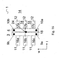
- Figure 16 shows a device comprising a sequence of semiconductor elements according to an embodiment of the invention.
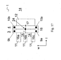
- Figure 17 shows a device comprising a sequence of semiconductor elements according to another embodiment of the invention.
- the device of the invention comprises a first and second semiconductor structure, preferably parts of a semiconductor substrate, and electrically coupled to a first and a second region, so that a current can be induced to flow from said first to said second region, via said structures.
- the semiconductor structures are placed adjacent each other, and are separated by an interface, e.g. a line between two zones in the substrate. Current will cross this interface, when said current is induced to flow between the first and second zone..
- the device of the invention further and characteristically comprises means to modulate the conductivity in at least one of said structures, so that if current flows across the interface, the current value will be a non-monotonic function of the location along said interface.
- the current has to resemble an impulse function along the interface, so that said current can flow only at a predefined position along said interface, and no current can flow at either side of said predefined position.
- the variation of the conductivity preferably takes on the form of a conductivity gradient, a continuous rise or fall of the conductivity along the interface. In that case, there is a gradient in both semiconductor structures, and the gradients are opposed to each other, i.e. if there is a rise in conductivity in one structure along a given direction, there is a fall in conductivity in the other structure along the same direction.
- the preferred embodiment is shown in figures 1 and 2 .
- the device is preferably but not necessarily a memory cell, based on a dual gate structure. It comprises a source and a drain region 11 and 12 (i.e. first and second region), separated by a channel region, consisting of a first and second part 16 and 17 (i.e. first and second semiconductor structure).
- Two separate and adjacent gate electrodes 5 and 7 (means for modulating conductivity) are present above these channel parts 16 and 17 respectively, and separated therefrom by dielectric layers 6 and 8, while being separated from each other by an insulation layer 18.
- at least one of these dielectric layers comprises a charge-storing layer 26, capable of receiving and storing an amount of charge.
- the gate electrodes 5 and 7 are longitudinal in shape and preferably placed immediately adjacent each other, i.e. spaced only by the insulating layer 18. The distance between the gate electrodes may be larger according to one particular embodiment however, as will be explained later.
- the 'width' direction of the device indicates the direction along the interface between the gate electrodes (direction W, see figure 1 ), corresponding to the width of the channel between source and drain.
- the 'length' of the device is measured in the direction perpendicular to that (direction L), i.e. corresponding to the length of said channel.
- the longitudinal direction of the gate electrodes themselves, i.e. defined by their shape, thus coincides with the W-direction. Left and right are only used to indicate opposite positions. First and second are only used to distinguish between similar structures at different locations. Similar features are designated using similar symbols throughout the description.
- Characteristic to the invention is the presence, on each of the electrodes 5 and 7, of two separate contacts (9a, 9b or 10a, 10b), on either side of these electrodes, along the width of the device.
- the contacts are arranged so that a different voltage can be applied to each of the contacts on one gate electrode.
- the idea is to introduce the possibility of applying a voltage gradient along the longitudinal direction of the gates, thereby creating the conductivity gradient mentioned above. As the voltage gradients are opposed to each other, and by the interaction of the gradients along both gate electrodes, one can thus create alternative paths for the source-drain current, in order to store a charge in a plurality of locations along the width of the gates. This general principle will hereafter be explained in more detail, based on a number of embodiments of the device and its methods of operation.
- the present invention thus discloses inter alia a memory cell capable of storing multiple bits along the width of the memory cell.
- the mechanism for addressing each individual bit in the memory cell is independent of the minimal feature size F of the technology.
- the number of bits in each cell is independent of the technology scaling.
- the memory cell only relies on common MOS (Metal-Oxide-Semiconductor) process technology and requires the formation of at least one additional contact to each of the gate electrodes.
- MOS Metal-Oxide-Semiconductor
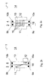
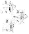
- FIG. 1 A cross section of a dual gate memory cell according to a first embodiment of the present invention is shown in figure 1 .
- the memory cell 1 comprises a semiconductor substrate 2 on which a first gate 3 and a second gate 4, adjacent to and insulated 18 from this first gate 3, are present.
- the first gate 3 comprises a first gate electrode 5 and a first gate dielectric 6 insulating the first gate electrode 5 from the semiconductor substrate 2.
- the second gate 4 comprises a second gate electrode 7 and a second gate dielectric 8 insulating the second gate electrode 7 from the semiconductor substrate 2.
- At least the second gate dielectric 8 comprises at least one charge-storing layer 26, e.g. a dielectric layer capable of storing charge thereon.
- the first gate dielectric 6 comprises at least one charge-storing layer, e.g.
- the memory cell illustrated by figure 1 comprises two gates, a first gate 3 and a second gate 4, the invention is not limited thereto.
- the memory cell can comprise more than two adjacent gates.
- Such a multiple gate memory cell can be formed using, for example the process sequence disclosed in US 6,580,120 , hereby incorporated by reference in its entirety.
- a contact (9a, 9b, 10a, 10b) is present, such that a voltage difference can be applied along the longitudinal direction of the first as well as of the second gate.
- these opposite contacts (9a and 9b, 10a and 10b) are not short-circuited or in direct ohmic contact and can be biased to the same or different voltages.
- on-chip biasing circuitry is foreseen to apply appropriate and selected voltages to each of the four contacts (9a and 9b, 10a and 10b).
- the voltage drop along this distance between these two opposite contacts determines the number of bits than can be stored within a memory cell according to the present invention.
- the memory cell further comprises a source region 11 and a drain region 12; the source region is lying adjacent to and extending at least partly along the first gate and the drain region lying adjacent to and at least partly extending along the second gate.
- the junctions formed in the source and drain region might partially extend under the adjacent gates.
- Figure 2a shows a schematic top view of the dual gate device illustrated by figure 1 .
- An active area 13 is shown, surrounded by insulating regions 14, better known as field regions.
- Two gates 3,4, parallel to and adjacent to each other, are formed over the active area 13, preferably parallel to the active area 13 and extending over the edges of the active area 13.
- a source region 11 and a drain region 12 are formed in the parts of the active area not covered by the gates.
- a contact (9a and 9b, 10a and 10b) is present, such that an electrical path is created from one end contact to the other end contact via the gate electrode contacted by these two corresponding end contacts.
- Figure 2b shows a schematic top view of a dual gate according to yet another embodiment of the present invention.
- two gates 3, 4 parallel to each other, are formed over the active area 13, preferably parallel to the active area and extending over the edges of the active area.
- a source region 11 and a drain region 12 are formed in the non-overlapped parts of the active area.
- a contact (9a and 9b, 10a and 10b) is present, such that an electrical path is created from one end contact to the other end contact via the gate contacted by these two corresponding end contacts.
- charge can be stored at any point in longitudinal direction (along W-axis) because the second gate dielectric 8, and optionally the first gate dielectric 7, comprises at least one continuous charge-storing layer, i.e. extending, capable of storing charge thereon.
- This charge-storing layer extends along the corresponding gate electrode, i.e. along the full longitudinal dimension of the gate.
- charge can be stored only at well-defined regions 15 along the longitudinal direction, as indicated by the spots.
- the charge-storing layer now consists of these individual, mutually isolated regions 15, each region capable of storing charge thereon, and each region will correspond to the position of a bit.
- regions 15 can be made of polysilicon and oxide can be used to insulate these polysilicon regions from each-other and from the substrate 2 and the gate electrode 7. Alternatively these regions can be made of nitride and oxide can be used to insulate these nitride regions from each other and from the substrate and the gate electrode. If a dielectric or another non-conductive material, e.g. nitride, is used to form the charge-storing layer, regions 15 at corresponding positions in adjacent gates can be connected as to form a strip of charge storing dielectric material in a direction perpendicular to the direction of the gate electrode. This way a grid structure is obtained comprising a first level of spaced apart strips 15 of a charge-storing dielectric and a second level of gate electrodes 3, 4. A person skilled in the art will realize that such regions 15 should be present at least underneath one gate electrode if the device of fig 2c is to be a memory device.
- the semiconductor substrate 2 can be a bulk silicon wafer, a silicon-on-insulator substrate or of any type of semiconductor substrates used by a person skilled in the art.
- the first gate 5 and second gate 7 electrodes can be formed of silicon. Typically polysilicon is used to form these gate electrodes.
- the first gate dielectric 6 can be formed of an oxide. In case of a silicon substrate 2, a silicon oxide is thermally grown on this substrate to form the first gate dielectric.
- the second gate dielectric 8 can be formed of a non-conductive material in which charge can be stored and which material is capable of locally storing and retaining charge injected to selected locations within this gate dielectric. This non-conductive material will prevent diffusion or displacement of the injected charge within this gate dielectric.
- charge-storing material typically silicon nitride is used as charge-storing material.
- this charge-storing dielectric is sandwiched in-between dielectric layers, which insulate the charge-storing dielectric from the substrate on the one hand and from the second gate electrode on the other hand.
- these sandwich dielectric layers are formed from silicon oxide.
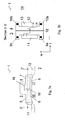
- Figure 3 shows a preferred embodiment of a memory cell according to the invention, namely a split gate SONOS cell.
- Figure 3a shows a schematic cross-section of this dual-gate device 1.
- the gate 3 at the source side 11 of the dual gate device uses silicon-oxide as gate dielectric 6, while the gate 4 at the drain side 12 uses an ONO (oxide-nitride-oxide) stack gate dielectric 8.
- ONO oxide-nitride-oxide
- the gate electrode 3 at the source side overlaps, at least partly, the gate electrode 4 at the drain side.
- the channel region formed in the substrate in between the source and the drain, consists of a first part 16 controlled by the source side gate 3 and a second part 17 controlled by the drain side gate 4.
- the source side gate 3 overlaps, at least partly, the drain side gate 4.
- Both gates of the dual-gate device are insulated from each-other by a dielectric 18 thereby yielding a capacitive coupling between both gates.
- At both ends, along the longitudinal direction, of each gate contacts are made.
- Each of these four contacts (9a and 9b, 10a and 10b) can be biased independently from the other contacts.
- each gate is widened at each end to offer sufficient space for forming a contact (9a and 9b, 10a and 10b) thereupon.
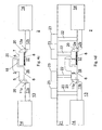
- Figure 4a illustrates a silicon substrate 2 comprising an active area 13 surrounded by field regions 14.
- this substrate pwell, nwell or other doped regions might be formed as will be appreciated and known by a person skilled in the art, in order to obtain regions having a giving conductivity type.
- the gate dielectric stack 8 of the second gate 4 is formed by growing an oxide on top of this substrate, followed by the deposition of a nitride layer and an oxide layer on top of this nitride layer. A polysilicon layer is deposited, which layer will be used to form the second gate electrode 7. This stack of oxide, nitride, oxide and polysilicon layers is patterned to form the second gate 4 in this active area. Then an oxide is grown which is used as gate dielectric 6 of the first gate 3, followed by the deposition of another polysilicon layer, which will be used to form the first gate electrode 5. This gate oxide is also grown on the polysilicon of the second gate and will therefore form an insulating layer 18 between the first 5 and second 7 gate electrode. This stack of oxide and polysilicon layers is patterned to form the first gate electrode 3 overlapping the second gate 4, as shown in figure 4b .
- An insulating layer 21 is deposited over the substrate, which layer will insulate the substrate and the devices present thereupon from the interconnect level formed later on.
- openings 22 are etched to expose the source 11 and drain 12 regions and both ends (9a and 9b, 10a and 10b) of each gate electrode 3,4. These openings 22 are filled with a metal to form a contact to the exposed regions.
- a metal layer 23 is deposited over this insulating layer and is then patterned to form a first interconnect pattern.
- Figure 4d shows the device at this stage of the processing. The sequence yielding figure 4d can be repeated as known by a person skilled in the art to form multiple interconnect levels, whereby the openings are etched in each dielectric layer to form a connective path between different interconnect levels.
- the invention is equally related to methods for operating a multibit memory cell according to the invention.
- methods for programming, reading and erasing the individual bits of the memory cell of the first aspect are disclosed.
- these prior art memory cells only allow storing a single bit along the width of the memory cell.
- the memory cell 1 of the present invention can be regarded as being a parallel connection of at least one dual gate structure, comprising a first gate 3 and a second gate 4. Underneath each gate 3, 4 a corresponding channel region 16, 17 is present.
- each channel region 16, 17 can, over at least a part of the device width, be inverted (regions 16a, 17a), while the remaining part of the channel region might be non-inverted (regions 16b, 17b). At that point in longitudinal direction where both inverted channel parts 16a, 17a overlap a bridge or cross-over point 24 is present.
- FIGs 6a to 6c illustrate the operation of the memory device of the invention, and the way in which it differs from prior art devices.
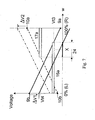
- the operation and layout of a conventional single-gate MOSFET is shown in figure 6a .
- the gate 3 of this transistor is biased at a single voltage yielding a substantially constant electrical potential along the gate electrode.
- a single contact 9a at one end of the gate is used to bias the gate electrode, but in case of long transistors multiple contacts to the gate can be used, but these contacts are linked to each-other as to yield a uniform electrical potential along the gate electrode.
- This uniform gate potential will create a uniform current flow I d in the channel, controlled by this gate electrode, from the source side to the drain side of the transistor, as indicated by the arrows of figure 6a .
- log Id logarithm of the channel current current
- the log Id curve is constant in this longitudinal direction. If both longitudinal ends 9a, 9b of this single-gate transistor are contacted and biased at different voltages, a voltage drop is created along the longitudinal direction of the gate electrode.
- This contact scheme is shown in figure 6b , where a voltage below the threshold voltage of the transistor is applied to the contact 9a at one end of the gate electrode, while a voltage above this threshold voltage is applied to the contact 9b at the opposite end of the gate electrode.
- the current flow I in the channel is no longer uniform along the width, but will vary in correspondence with the variation in the gate electrode potential. Only in these channel regions 16a (dotted area) where the corresponding gate potential is above threshold an inversion region is formed and current will flow, while in remaining part 16b (white area) of the channel no current will flow, as this part is not inverted. In the log Id curve in the top part of figure 6b , this is illustrated by the fact that at the border between the inverted 16a and non-inverted 16b part of the channel the current drastically drops.
- FIG. 6c shows the dual-gate memory cell according to the present invention.
- each gate electrode 3, 4 is contacted at both ends (9a and 9b, 10a and 10b) and at each contact a different voltage can be applied, such that a voltage gradient, in this case a voltage drop from one contact to the other, is created over each gate electrode.
- the potential drop of the adjacent gate electrodes is in opposite direction, meaning that, if the gate voltage increases along one gate electrode (in case of gate 3 increases from 9a towards 9b), it decreases along the adjacent gate electrode (in case of gate 4 decreases from 10a towards 10b).
- current will only flow from the source to the drain side if the inversion region created by a voltage of the first gate at least partly overlaps 24 with the inversion region created by a voltage of the second gate.
- Figure 7 illustrates for both gate electrodes the variation in gate voltage along the width of the device. Whereas the voltage along the first gate 3 (higher thick solid curve in figure 7 ) decreases when going from left 9b to right 9a in figure 6 , the voltage along the second gate 4 (lower thick dashed curve in figure 7 ) increases when going from left 10b to right 10a in figure 6 .
- the slope of each voltage curve will depend on the voltage difference applied over each gate electrode, the length of each gate and on change of the resistance of the gate electrode along its length. Selecting the appropriate material or material composition can modify the latter: e.g. metal lines, polylines that can be fully or partially silicided in longitudinal direction.
- the resistance of the gate electrode can also be voltage dependent, e.g.
- a lowly doped polysilicon layer is used as gate electrode material.
- this layer will be depleted, the degree of depletion at each point being dependent upon the doping level and the electrical potential at that point.
- a linear voltage drop over the gate electrode is assumed, although the invention is not limited thereto.
- a second inversion region 17a is created in the second channel 17, i.e. the channel controlled by the second gate 4, where the gate voltage is above threshold: Vgd >Vt4, as the drain side 12 is biased to a voltage Vd.
- An overlap 24 between both inversion regions exists at the crossover of both gate voltages in a region where both gate voltages are above or about their corresponding threshold voltages.
- the crossover point 24 can be moved to the left side of the device by decreasing the voltages applied to the end contacts 9a and 9b by an amount ⁇ V and increasing the voltages applied to the end contacts 10a and 10b by the same amount ⁇ V as illustrated by the lowering of the thick line by ⁇ V1 and by raising the dotted line by ⁇ V2, the crossover point being shifted to the left.
- ⁇ V1 and ⁇ V2 can be equal to each other.
- a voltage difference is applied to both gate electrodes, necessitating the need for an electrical contact at each end, as is illustrated in figure 2a
- the crossover point in this case is defined as the region where the gate voltage of the gate to which a voltage difference is applied is above or about its corresponding threshold voltage.
- the first channel region is pinched off at the drain side of the first gate, inducing a large lateral electrical field at the border between the first and the second gate.
- This large lateral electrical field creates hot electrons, which are swept into the ONO dielectric at the source side of the second gate, also labelled as the carrier injection point, due to the large bias voltage on this second gate. This completes the program operation.
- a high bias voltage is applied to the first gate thereby creating an inversion region in the first channel.
- This inversion region will act as a virtual source underneath this first gate.
- Moderate voltages are applied to the second gate and to the drain.
- Charge trapped in the ONO stack at the source side of the second gate will now modulate the potential barrier of the virtual source towards the second channel region and hence the overall current flowing through the device.
- the gate dielectric of the first gate can consist of an ONO-dielectric stack thereby rendering the memory cell symmetric. Hence a bit can be stored underneath the first and/or second gate electrode, allowing up to two bits to be stored in the cell in the width direction.
- hot holes are generated near the drain side and injected into the ONO stack to compensate the electrical charge stored in the ONO stack during programming.
- a negative bias is applied to the second gate in order to attract the holes generated near the drain, by band-to-band tunneling.
- a slightly positive voltage is applied to the first gate to repel these hot holes from drifting towards this first gate.
- FIG 8 one can apply the above operating mechanisms to a memory device according to the present invention.
- a cross-over region 24a along the gates of this memory cell is selected according to the present invention on the memory cell.
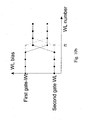
- the potential drop of the adjacent first 3 and second 4 gate electrodes are in opposite direction or alternatively a potential pulse is applied to the first gate 3 only while a constant voltage is applied to the second gate 4 as illustrated by the voltage biasing scheme depicted in figure 15 .
- the current I flowing from the source 11 towards the drain 12 can be forced to run across the spacing 18 between the first gate 3 and the second gate 4 at a well-defined region 24a along the width of the transistor, as indicated by the arrows in figure 8b .
- this region 24a hot electrons will be injected into the ONO stack of the second gate as explained above.
- the logarithm of the injection current (log Iinj) is given as function of the position along the width of the device.
- the hot electron injection current into the gate dielectric is a function of the device current: only at or near the overlap region 24a the channel current can provide sufficient hot carriers to be injected into the gate dielectric.
- the hot carrier injection also requires a large lateral field at the drain side of the first gate 3.
- This large lateral field occurs at the point 24b where the gate voltage of the first gate 3 is at or slightly above its corresponding threshold voltage.
- a similar lateral electrical field distribution assisting in injection of carriers into the gate dielectric can be obtained when a constant voltage is applied to gate 4 while a voltage gradient is applied to gate 3. In this way a bit is stored at the selected position of the injection point 24b.
- Increasing the drain 12 and bias voltage at the second gate 4 can accomplish the writing of charge at this selected spot along the width of the memory cell. This increased bias will increase the lateral field at the border between the first 3 and the second 4 gates and allow hot electron injection into the ONO-dielectric 8.
- Appropriate biasing allows this injection current Iinj to have a sharp maximum at a small spot along the width of the memory cell as shown in the log Iinj plot.
- Simultaneously ramping up the voltages at the end contacts, e.g. first gate contacts 9a, 9b, of one gate, e.g. the first gate 3, and optionally ramping down the voltages at the end contacts, e.g. second gate contacts 10a, 10b, of the adjacent gate, e.g. second gate 4 moves this injection point 24 in longitudinal direction up or down. Consequently at each selected crossover point electrons can be injected resulting in a series of bits stored in longitudinal direction of the multibit memory cell, as indicated by the round black spots in figure 8b .
- a selected bit in the multibit split-gate SONOS memory cell of the invention can be read, by applying a low drain bias, while the bit can be selected by applying appropriate voltage drops over both gates to have the crossover point substantially coinciding with the position of the bit to be read. Finally, erasing of the entire channel can be accomplished in the same way as described for the single bit split-gate SONOS cell.
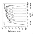
- Measurements have been performed on a prototype n-type memory cell according the preferred embodiment with 5/10/5nm ONO (7) and 12nm oxide dielectric (5) underneath the second 4 and first gate 3 respectively.
- the memory cell has a salicided first 3 and second gate 4 with drain- and source-side gate lengths of 0.2 ⁇ m and 0.3 ⁇ m, respectively, and a device width Wcell of 100 ⁇ m.
- the measurements have been performed with voltage drops over the first and the second gate of 5V, a drain bias of 5V for programming with a 100 ⁇ s programming drain pulse and a drain bias of 1V for reading. These values have been selected for demonstration purposes but have not been optimized for memory operation.
- Figure 9 gives the experimental results obtained on a memory cell according the preferred embodiment.
- bits are subsequently programmed, read and erased before programming another bit.
- the measured drain current as function of the position w (%) of the cross-over point, are plotted in figure 9 one on top of another.
- the magnitude of the drain current will than be indicative for the value of this bit.
- the width of the peak of each curve in 9 is defined by a 10 times drop in current relative to the peak value of this curve.
- This peak width is viewed as the spatial distribution of the charge stored at that position.
- This peak width corresponds to a voltage drop of about 630mV. If the total gate differential voltage, i.e. the voltage drop over each of the two gates, is kept constant at 5V, such voltage drop results in a peak-width of 12.6% of the device width: 630mV/5V. Taking the bit pitch equal to half of the peak-width, allowing about 10% interference of overlap between adjacent bits, ca. 15 bits can be stored in a single cell.
- This first-order assessment predicts that the number of bits per cell is proportional to the voltage drop along the gate and independent of the device width Wcell, hence the physical bit spacing can be made arbitrarily small by reducing the device width Wcell. Practically, the bit density will be limited by the properties of the trapping medium, e.g. diffusion of the injected charge. Hence, the present invention offers the opportunity for obtaining a pitch between bits in a memory cell to be below the lithography feature size F.
- layouts for a memory matrix comprising the memory cell according to the present invention are disclosed.
- FIG 10a a possible array-layout for such a memory matrix is shown.
- the memory cell 1 is within the dashed area and has a layout similar to the layout of the memory cell shown in figure 3b .
- Source 11 and drain 12 strips run vertically, first 3 and second 4 poly gates are contacted by metal word-lines running in perpendicular to the source and drain strips (not shown). Separate word-lines are required to respectively contact the first gate and the second gate.
- contacts (9a and 9b, 10a and 10b) are put on the poly lines within the active area 13 region.
- the contacts to the first and the second gate are at a spacing of about 2F as indicated in figure 10a .
- the source 11 and drain 12 regions run underneath the contact regions of the poly lines.
- figure 10b a biasing scheme for the layout of figure 10 is proposed. Only one row of gate electrodes is biased at a time. The word-line bias on other rows is constant so that no current will flow through the gate electrodes of non-selected rows.
- figure 10a thin lines
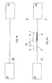
- a device of the invention is preferably, but not necessarily, a memory cell.
- the distance between the gates 3 and 4 is not determined. For a memory cell working as described above, this distance is preferably not larger than the thickness of the insulating layer 18. However, when the gates are spaced further apart, other components may be placed in the space between the gates.
- the memory device of the present invention comprises a first 3 and a second gate 4 between the source 11 and drain 12 regions. Thanks to the biasing of this first 3 and second 4 gate a current will flow between the source 11 and drain 12 regions at a well-defined position 24 between this first 3 and second 4 gate.
- this current bridge 24 can be shifted along the width of the memory device and selected points can be addressed. If the first and second gates are spaced apart other devices 25 or structures can be inserted in between the first 3 and second 4 gate. The biasing of this first and second gate is then used to control the position at which current will flow through or in the vicinity of this intermediate structure.
- a device according to this embodiment can be used to control, sense or influence the operation or physical state of this intermediate element at selected points.
- This intermediate element can be formed in the substrate, e.g. as trench in-between the first and the second channel which is filled with a selected material. It can also be formed upon the substrate in-between the first and second gate.
- This intermediate element can have a continuous character, e.g. formed as a strip of material, or can consist of discrete elements, e.g. separate blocks of material or an array of individual components such as sensors which are located at predefined positions along the width of the dual selection structure.
- Figure 11a schematically illustrates the general concept of this dual gate structure by means of schematic cross-section.
- a first gate 3 is present.
- this gate will comprise a gate electrode 5 and a gate dielectric 6, but person skilled in the art will realize that other types of Field Effect Transistor (FET) structure can be used as selecting element 3.
- FET Field Effect Transistor
- a second gate 4 is present, which in case of a MOSFET will comprise a gate electrode 7 and a gate dielectric 8.
- an element 25 can be inserted, which is associated with the current Id flow between the source and drain under control of the first and second gate, when biased as disclosed in the third aspect of the invention.
- the current flow at the selected point 24 might influence or sense the operation or status of the element 25 in a direct or indirect way.
- a charge trapping medium 25 is inserted in between the first and the second gate. Instead of injecting the charge into the charge storage layer of either the first and/or the second gate, as was the case in the preferred embodiment of the third aspect illustrated by figure 8 , current Iinj is now injected into this trapping medium 25.
- the charge trapping medium can be formed as a continuous strip of material 25 extending along the width of the device, as shown in figure 11c , or it can be formed as a number of well-defined regions or as a sequence of individual elements (25a, 25b, 25c) placed adjacent to each other along the width of the device and separated from one another by an insulating material 27 such as oxide, as shown in figure 11d .
- This trapping medium can be nanocrystals such as polysilicon or metal dots embedded in an insulating layer such as oxide, high-k dielectrics such as Al2O3 or nitride. If the charge trapping medium is in the form of such well-defined mutually isolated regions (25a, 25b, 25c), the charge trapping medium can also be made of a conductor such as polysilicon or a metal.
- the intermediate element 25 is a strip of a resistance-changing material formed in the substrate in between the first 3 and second gate 4. If a high current passes through such a resistance-changing material physical or structural changes occur within the material thereby changing its resistivity. This resistivity change can then afterwards be detected by the impact this resistivity change has on a sense current flowing through this intermediate element 25, the current level of this sense current being chosen to be sufficiently low in order not to change the resisitivity of the intermediate element 25.. This known effect is explored in memory devices, as the low and high resistivity state corresponds to respectively an unprogrammed and a programmed bit. By locally changing the resistance of this strip 25 of resistance-changing material, i.e.
- a bit can be programmed at this selected position.
- the state of the bit can be detected.
- resistance-changing materials are known in the art, e.g. chalcogenide or perovskite materials.
- Ron Neale discloses in " Amorphous non-volatile memory: the past and the future" in Electronic Engineering, vol 73, no 891, pp67-78, 2001 hereby incorporated by reference in its enterity the use of such phase-changing chalcogenide materials. The phase structure of this materials changes at higher current levels flowing through it and hence its resistivity will change accordingly.
- an array of sensors 25 is placed as a sequence of intermediate element in-between the first gate 3 and the second gate 4.
- the sensing element 25 can also comprise a continuous structure extending along the width of the device.
- This eminascent electromagnetic field can be detected by and trigger the operation of this sensor element or this field can in turn be influenced by the sensor element.
- This sensor element can be an optical device, a chemical or a magnetic sensor.
- the sensor element can be coupled to the current Id by modulating the conductivity of the semiconducting substrate below the sensor and in between the first 16 and the second 17 semiconductor regions.
- the conductivity modulation induced by the sensor element 25 can be detected locally at the position of the current bridge 24.
- This conductivity modulation can be caused by electromagnetic radiation, e.g. visible light, by creation of electron-hole pairs in the semiconductor substrate.
- the sensor element 25 can guide electromagnetic radiation originating from the environment to the semiconductor substrate, e.g. it can comprise a lens, an optical filter or a transparant medium such as oxide.
- the transparency of this medium can be modulated by physical quantities originating from the environment, e.g. the sensor element 25 can comprise liquid crystals that respond to an external electrostatic or magnetic field.
- the sensor element 25 can also change the wavelength of the electromagnetic radiation originating from the environment to a wavelength that is more suitable for the creation of electron-hole pairs in the substrate.
- the sensor element 25 can comprise a phosphorescent material.
- An alternative method to couple the current Id flowing in the semiconductor substrate to the sensor element is by means of an electrostatic field.
- external physical quantities can induce a charge or a charge dipole in the sensing element 25. This charge or charge dipole will create an electrostatic field which will then in turn modulate the conductivity in the substrate by the field-effect.
- Such external physical quantities can be chemical species or electromagnetic radiation.
- US patent 6,521,109 discloses various ways of how such a chemical quantity can modify the operation of a field-effect-transistor, in a general way in the background section and in the description for a so-called CHEMFET. Bergveld, IEEE Transactions on Biomedical Engineering MD-17, 1970, pp.
- the senor 25 can comprise a photo-diode. Light falling into this photo-diode will generate a current which can be used to induce a net charge in vicinity of the semiconductor substrate.
- the element 25 can also be an actuating device, i.e. it can translate an electrical signal into a physical quantity propagating to the external environment. This electrical signal can be, or can be generated, controlled or triggered by the current Id flowing in the current bridge 24.
- the actuating element 25 could comprise a light emitting device. In this example the actuator 25 could be partly or entirely placed in-between the semiconductor structures 16 and 17, as shown in figure 11a , so that a current is flowing through the actuator 25 at the position of the current bridge 24.
- the choice of electrode material(s) also determines the electrical field distribution in the gate electrode 5, 7 in longitudinal direction and the conductivity gradient induced by this electrical field in the corresponding substrate region 16, 17.
- this choice will be discussed in more detail for the first gate 3, however the application of this teaching can also be applied to the other gate 4.
- polycrystalline silicon would be a first choice for the electrode material. This material can be easily integrated in a semiconductor device while its resistivity can be modulated by selecting an appropriate implantation species and dose.
- Lowly doped polysilicon is an example of a material whereby its resistivity depends on the voltage applied to it.
- Such voltage-controlled-resistors can thus be used to transform the voltage difference applied over the gate electrode into a non-linear electrical field distribution and, preferably, result in a sharper voltage drop at particular locations along the longitudinal direction thereby reducing the width of the overlap region 24.
- Using polycrystalline as gate electrode material would also allow the formation a so-called PIN diode in the gate electrode. The operation of such a PIN device is explained by Sze in "Physics of semiconductor devices", 1981 Wiley&Sons, p. 117 to p. 122, hereby incorporated by reference in its entirety. This is illustrated in figure 13 .
- a depletion region is created between a p-type doped and n-type semiconductor region.
- the gate electrode is constructed from a p-doped region 5c, in this example located near the contact region 9a, and a n-doped region 5d located near the contact region 9b. Both regions are separated by an undoped or intrinsic semiconductor region 5e.
- undoped semiconductor region 5e can also be formed by a high resistive n-type or p-type doped region.
- a PIN structure is thus created by combination of p-type doped region 5c, undoped region 5e and n-type doped region 5d.
- the depletion region of such PIN structure will be located within the undoped region 5e.
- the voltage between both contacts 9a and 9b will vary in a non-linear way as illustrated by the voltage V -longitudinal position W - curve of figure 13 .
- the resistivity of the depletion layer formed within region 5e will depend on the voltage applied over the PIN diode as shown in figure 41, p 119 of the Sze reference.
- material(s) with a high resistivity reduces the current flow through the gate electrode when applying the voltage difference thereover, resulting in a decreased power consumption during operation.
- the number of distinct overlap regions 24 can also be increased by optimising the layout of the device 1.
- a device 1 is shown having the interface between the two substrate regions 16, 17 run in one particular direction.
- Figure 14 shows an alternative layout for the device 1.
- the device 1 is designed as a serpentine structure.
- Other layouts allowing an increase of the length of the interface, for given dimensions of the active area 13, are known in the art.
- Figure 15 illustrates an alternative-biasing scheme compared to figure 7 .
- the voltage drops linearly with the position w in longitudinal direction W resulting in a similar monotonic conductivity change in the corresponding substrate regions 16, 17.
- the inversion regions 16a, 17a of both semiconductor regions coincide thereby allowing the current to flow from the first contact region 11 to the second contact region 12 through this overlap region 24.
- a non-monotonic current flow is generated from the first contact region 11 towards the second contact region 12 through the interface between the semiconductor regions 16 and 17.
- the same confined current flow between first 11 and second 12 contact region can be obtained by applying a biasing scheme as illustrated in figure 15 .
- One gate electrode can be biased to a constant voltage above the threshold voltage Vt4 of the second gate 4 such that an inversion region is created underneath this gate electrode 4 over the complete semiconductor region 17.
- no voltage is applied, or at least no voltage above the threshold voltage of the first gate 3
- no inversion region is created in the corresponding parts of the semiconductor region 16 and a non-monotonic conductivity change is created in semiconductor region 16 resulting again in a non-monotonic or peak current from the first contact region to the second contact region through the interface between both semiconductor regions 16, 17.
- current can only flow within the inverted region 16a underneath the voltage pulse applied at the first electrode 5 towards the second gate 4.
- the combination of the biasing of gate electrode 5 and gate electrode 7 thus results in a current flow between both contact regions 11, 12 at a predetermined position 24.
- the semiconductor regions 16, 17 were assumed to be continuous semiconductor regions.
- a semiconductor substrate 2 e.g. silicon
- Figure 1 can be viewed as a cross-section 2-2 of figure 2a in length direction i.e. along the L-axis.
- the semiconductor regions 16, 17 can be formed.
- a p-type doped substrate one can form by e.g. ion implantation p-well semiconductor regions in case nMOS Field Effect Transistor (FET)-devices are to be manufactured or n-well semiconductor regions in case pMOS FET devices are to be created upon this substrate.
- FET Field Effect Transistor
- the semiconductor regions 16, 17 are isotropic and continuous at least in longitudinal direction W.
- the invention is not limited to such continuous semiconductor regions 16, 17.
- the semiconductor regions 16, 17 or at least one of them can be formed as a sequence of semiconducting elements 16a-17a, 16b-17b, 16c-17c which are electrically insulated from each other.
- the active area 13 of figure 2a is replaced by strips of semiconducting regions 16a-17a, 16b-17b, 16c-17c. Each strip will have a first contact region 11, e.g. source, and a second contact region 12, e.g.
- One way of forming such a sequence of individual semiconductor regions 16a-17a, 16b-17b, 16c-17c is to form parallel active area regions 13 in a semiconductor substrate 1, these active area regions being insulated by a dielectric 14. In a direction substantially perpendicular to these semiconducting strips the gate structures 3 and 4 are created overlapping all these semiconducting strips.
- This semiconducting strip 16a-17a, 16b-17b, 16c-17c can be the fin (17) of a FinFET device as disclosed in European application EP 1 383 166 .
- the fin (17) is a silicon strip formed in a silicon layer (2) upon the oxide layer (3) of an SOI substrate (1).
- This semiconducting strip 16a-17a, 16b-17b, 16c-17c can be a semiconductive polymer, e.g. an organic polymer such as a carbon nanotubes, deposited on a non-conductive substrate 2. Such carbon nanotubes are known in the art. R.
- the device illustrated in figure 16 does generally operate in a way similar to the device illustrated in figure 2a . As indicated by the arrows, current I will flow from one contact region 11 to another contact region 12 at a predetermined point 24 along the interface between the corresponding semiconducting regions 16a-17a, 16b-17b, 16c-17c.
- the difference in operation of the device of figure 16 compared to the device of figure 2a is that not every point 24 in longitudinal direction can be selected, but only points that lie within such a semiconductor strip 16a-17a, 16b-17b, 16c-17c.
- the electrical field distribution in gate 3 and 4 is selected such that both semiconducting regions 16b-17b are conducting thereby forming a conductive path between the corresponding contact regions 11 and 12.
- both regions 16a-17a, 16c-17c at least one of these semiconducting regions is biased in a non-conductive state, e.g. depletion.
- both regions can be biased in a conductive state but with inverse polarity, i.e. conduction is based on transport of charge carriers of an opposite conductivity type.
- semiconducting region 16a might be biased into inversion with electrons as carriers, while corresponding semiconducting region 17a is biased into accumulation with holes as carriers. Consequently an energy barrier is created at the interface between both semiconducting regions 16a, 17a blocking the flow of carriers from one contact region 11 to the other contact region 12.
- Figure 17 illustrates another alternative structure.
- the semiconductor region 16 underneath the first gate 3 is constructed as a sequence of semiconductor elements 16a, 16b, 16c, each element having its own contact region 11 while the semiconductor region 17 underneath the second gate is formed as a continuous region extending along the longitudinal direction.
- the gate structures 3, 4 are still continuous in longitudinal direction in all embodiments discussed.
Landscapes
- Engineering & Computer Science (AREA)
- Chemical & Material Sciences (AREA)
- Nanotechnology (AREA)
- Physics & Mathematics (AREA)
- Mathematical Physics (AREA)
- Theoretical Computer Science (AREA)
- Crystallography & Structural Chemistry (AREA)
- Computer Hardware Design (AREA)
- Non-Volatile Memory (AREA)
- Semiconductor Memories (AREA)
Claims (20)
- Halbleitervorrichtung, umfassend:eine erste Halbleiterstruktur (16) in elektrischem Kontakt mit einem ersten Kontaktgebiet (11),eine zweite Halbleiterstruktur (17) in elektrischem Kontakt mit einem zweiten Kontaktgebiet (12),wobei die erste Halbleiterstruktur (16) und die zweite Halbleiterstruktur (17) an einer Schnittstelle entlang miteinander in elektrischem Kontakt stehen,
dadurch gekennzeichnet, dass die Vorrichtung ferner Mittel (3, 4) zum Modulieren der Leitfähigkeit in mindestens einer der Halbleiterstrukturen umfasst, so dass die Leitfähigkeit an der Schnittstelle entlang derart variiert, dass wenn Strom durch die Schnittstelle fließt, dieser Strom nur an einer vorher bestimmten Position (24) an der Schnittstelle entlang fließen kann, und im Wesentlichen kein Strom auf beiden Seiten der vorher bestimmten Position fließen kann. - Halbleitervorrichtung nach Anspruch 1, wobei die Modulationsmittel (3, 4) dazu geeignet sind, um einen Gradienten der Leitfähigkeit in jeder der Halbleiterstrukturen (16, 17) in der Schnittstellenrichtung hervorzurufen, wobei die Gradienten einander entgegengesetzt sind, so dass wenn eine stetige Zunahme der Leitfähigkeit in einer Struktur in einer bestimmten Richtung an der Schnittstelle entlang vorliegt, eine stetige Abnahme der Leitfähigkeit in der anderen Struktur in der gleichen Richtung vorliegt.
- Halbleitervorrichtung nach Anspruch 1 oder 2, wobei die ersten und zweiten Kontaktgebiete eine Source (11) und einen Drain (12) bilden, und wobei die Halbleiterstrukturen (16, 17) ein Kanalgebiet zwischen der Source und dem Drain bilden, wobei die Vorrichtung mindestens zwei Steuerelektroden (5, 7) umfasst, die elektrisch voneinander isoliert sind, wobei jede Steuerelektrode mit einer der Halbleiterstrukturen (16, 17) des Kanalgebiets dielektrisch gekoppelt ist, dadurch gekennzeichnet, dass jede der Steuerelektroden mit zwei Kontaktpunkten (9a, 9b) versehen ist, die derart angeordnet sind, dass sie das Anlegen von zwei verschiedenen Spannungspegeln an diese beiden Kontakte gestatten, um dadurch einen Spannungsgradienten in der Steuerelektrode zu schaffen.
- Halbleitervorrichtung nach Anspruch 3, wobei die Steuerelektroden länglich geformt sind, und wobei die Kontakte (9a, 9b) auf den beiden Enden der mindestens einen Steuerelektrode bereitgestellt werden.
- Vorrichtung nach Anspruch 4, wobei die Steuerelektroden (5, 7) in unmittelbarer Nähe zueinander angeordnet und durch einer Isolationsschicht (18) beabstandet sind.
- Vorrichtung nach Anspruch 4, wobei die Steuerelektroden (5, 7) in einem bestimmten Abstand voneinander angeordnet sind, wobei ein Zwischenelement (25) dazwischen angeordnet ist.
- Vorrichtung nach Anspruch 6, wobei das Zwischenelement ein Erfassungs-/Betätigungselement, ein Haftmedium, wie etwa Nanokristalle, oder ein Streifen eines widerstandsändernden Materials ist.
- Vorrichtung nach einem der Ansprüche 1 bis 5, wobei mindestens eine der dielektrischen Schichten eine Ladungsspeicherungsschicht (26) umfasst.
- Vorrichtung nach Anspruch 8, wobei die Ladungsspeicherungsschicht Siliziumnitrid umfasst.
- Vorrichtung nach Anspruch 8, wobei die Ladungsspeicherungsschicht aus diskreten Gebieten (15) eines Materials besteht, das dazu geeignet ist, eine Ladung darauf zu speichern.
- Vorrichtung nach Anspruch 1, wobei die Halbleiterstrukturen (16, 17) als ein durchgehendes Gebiet in einem Substrat gebildet sind.
- Vorrichtung nach Anspruch 1, wobei die mindestens eine der Halbleiterstrukturen (16, 17) als eine Reihe von Halbleiterelementen (16a-17a, 16b-17b, 16c-17c, ...) gebildet ist, die elektrisch voneinander isoliert sind.
- Vorrichtung nach Anspruch 12, wobei die Halbleiterelemente in einem Substrat gebildete Halbleitergebiete sind.
- Vorrichtung nach Anspruch 12, wobei die Halbleiterelemente halbleitende Kohlenstoffnanortihren sind, die auf einem Substrat (2) gebildet sind.
- Vorrichtung nach einem der Ansprüche 3 bis 14, wobei mindestens eine der Steuerelektroden aus schwach dotiertem Silizium hergestellt wird.
- Vorrichtung nach einem der Ansprüche 3 bis 14, wobei mindestens eine der Steuerelektroden eine PIN-Diode ist.
- Vorrichtung nach einem der Ansprüche 3 bis 14, wobei mindestens eine der Steuerelektroden aus TaN hergestellt wird.
- Vorrichtung nach einem der Ansprüche 3 bis 14, wobei mindestens eine der Steuerelektroden als ein Materialstapel gebildet wird.
- Verfahren zum Betrieb einer Vorrichtung nach einem der Ansprüche 1 bis 14, wobei das Verfahren folgende Schritte umfasst:Schaffen einer vorher bestimmten Änderung der Leitfähigkeit in der Richtung der Schnittstelle in mindestens einer der Halbleiterstrukturen (16),Anpassen der Änderung(en) der Leitfähigkeit auf eine Art und Weise, die es erlaubt, Strom von dem ersten Kontaktgebiet (11) durch die erste (16) und die zweite (17) Halbleiterstruktur bis zum zweiten Kontaktgebiet (12) fließen zu lassen, wobei der Stromfluss an einer vorher bestimmten Position (24) an der Schnittstelle entlang erfolgt.
- Verfahren nach Anspruch 19, wobei ein Gradient der Leitfähigkeit in den beiden Halbleiterstrukturen erstellt wird, wobei die Gradienten entgegengesetzt sind, so dass wenn eine stetige Zunahme der Leitfähigkeit in einer Struktur in einer bestimmten Richtung an der Schnittstelle entlang vorliegt, eine Abnahme der Leitfähigkeit in der anderen Struktur in der gleichen Richtung vorliegt.
Applications Claiming Priority (2)
| Application Number | Priority Date | Filing Date | Title |
|---|---|---|---|
| US53212903P | 2003-12-23 | 2003-12-23 | |
| US532129P | 2003-12-23 |
Publications (3)
| Publication Number | Publication Date |
|---|---|
| EP1548842A2 EP1548842A2 (de) | 2005-06-29 |
| EP1548842A3 EP1548842A3 (de) | 2008-10-15 |
| EP1548842B1 true EP1548842B1 (de) | 2009-06-10 |
Family
ID=34549620
Family Applications (1)
| Application Number | Title | Priority Date | Filing Date |
|---|---|---|---|
| EP04447293A Expired - Lifetime EP1548842B1 (de) | 2003-12-23 | 2004-12-22 | Nichtflüchtige Multibit-Speicherzelle und deren Herstellungsverfahren |
Country Status (5)
| Country | Link |
|---|---|
| US (1) | US7569882B2 (de) |
| EP (1) | EP1548842B1 (de) |
| JP (1) | JP5150860B2 (de) |
| AT (1) | ATE433604T1 (de) |
| DE (1) | DE602004021465D1 (de) |
Families Citing this family (25)
| Publication number | Priority date | Publication date | Assignee | Title |
|---|---|---|---|---|
| US6753590B2 (en) * | 2002-07-08 | 2004-06-22 | International Business Machines Corporation | High impedance antifuse |
| US7456476B2 (en) | 2003-06-27 | 2008-11-25 | Intel Corporation | Nonplanar semiconductor device with partially or fully wrapped around gate electrode and methods of fabrication |
| US7221597B2 (en) * | 2004-05-26 | 2007-05-22 | Micron Technology, Inc. | Ballistic direct injection flash memory cell on strained silicon structures |
| US7042009B2 (en) | 2004-06-30 | 2006-05-09 | Intel Corporation | High mobility tri-gate devices and methods of fabrication |
| US20060086977A1 (en) | 2004-10-25 | 2006-04-27 | Uday Shah | Nonplanar device with thinned lower body portion and method of fabrication |
| US7518196B2 (en) | 2005-02-23 | 2009-04-14 | Intel Corporation | Field effect transistor with narrow bandgap source and drain regions and method of fabrication |
| WO2006090458A1 (ja) * | 2005-02-24 | 2006-08-31 | Spansion Llc | 半導体装置及びその製造方法 |
| US7858481B2 (en) | 2005-06-15 | 2010-12-28 | Intel Corporation | Method for fabricating transistor with thinned channel |
| US7547637B2 (en) | 2005-06-21 | 2009-06-16 | Intel Corporation | Methods for patterning a semiconductor film |
| US7279375B2 (en) * | 2005-06-30 | 2007-10-09 | Intel Corporation | Block contact architectures for nanoscale channel transistors |
| DE102005039365B4 (de) * | 2005-08-19 | 2022-02-10 | Infineon Technologies Ag | Gate-gesteuertes Fin-Widerstandselement, welches als pinch - resistor arbeitet, zur Verwendung als ESD-Schutzelement in einem elektrischen Schaltkreis und Einrichtung zum Schutz vor elektrostatischen Entladungen in einem elektrischen Schaltkreis |
| US20070090416A1 (en) | 2005-09-28 | 2007-04-26 | Doyle Brian S | CMOS devices with a single work function gate electrode and method of fabrication |
| US7485503B2 (en) | 2005-11-30 | 2009-02-03 | Intel Corporation | Dielectric interface for group III-V semiconductor device |
| US8143646B2 (en) | 2006-08-02 | 2012-03-27 | Intel Corporation | Stacking fault and twin blocking barrier for integrating III-V on Si |
| US20080149970A1 (en) * | 2006-12-21 | 2008-06-26 | Thomas Shawn G | Multi-gated carbon nanotube field effect transistor |
| US8362566B2 (en) | 2008-06-23 | 2013-01-29 | Intel Corporation | Stress in trigate devices using complimentary gate fill materials |
| US7692972B1 (en) | 2008-07-22 | 2010-04-06 | Actel Corporation | Split gate memory cell for programmable circuit device |
| KR101064593B1 (ko) | 2009-05-12 | 2011-09-15 | 고려대학교 산학협력단 | 1셀 4비트의 비휘발성 메모리 소자 및 그 제조 방법 |
| US9263132B2 (en) * | 2011-08-10 | 2016-02-16 | Globalfoundries Singapore Pte. Ltd. | Double gated flash memory |
| US8610241B1 (en) * | 2012-06-12 | 2013-12-17 | Taiwan Semiconductor Manufacturing Company, Ltd. | Homo-junction diode structures using fin field effect transistor processing |
| US8930866B2 (en) | 2013-03-11 | 2015-01-06 | Taiwan Semiconductor Manufacturing Company, Ltd. | Method of converting between non-volatile memory technologies and system for implementing the method |
| WO2015043610A1 (en) * | 2013-09-24 | 2015-04-02 | Khalel Abdel-Rahman Tharwat Refai | Pn-junction diode with multiple contacts and analog-to-digital converter using it |
| US9425055B2 (en) * | 2014-05-28 | 2016-08-23 | Freescale Semiconductor, Inc. | Split gate memory cell with a layer of nanocrystals with improved erase performance |
| CN105970257B (zh) * | 2016-06-30 | 2018-12-25 | 中国计量大学 | 一种铁-锰-磷磁性合金电镀液及其制备方法 |
| CN114121071B (zh) * | 2020-08-25 | 2026-02-03 | 格科微电子(上海)有限公司 | 多位半导体存储单元、存储阵列及其操作方法 |
Family Cites Families (14)
| Publication number | Priority date | Publication date | Assignee | Title |
|---|---|---|---|---|
| US4334292A (en) * | 1980-05-27 | 1982-06-08 | International Business Machines Corp. | Low voltage electrically erasable programmable read only memory |
| US4998147A (en) * | 1989-07-31 | 1991-03-05 | Motorola, Inc. | Field effect attenuator devices having controlled electrical lengths |
| US5739065A (en) * | 1995-10-13 | 1998-04-14 | United Microelectronics Corp. | Method of fabricating a highly sensitive photo sensor |
| US6177333B1 (en) * | 1999-01-14 | 2001-01-23 | Micron Technology, Inc. | Method for making a trench isolation for semiconductor devices |
| US6255166B1 (en) * | 1999-08-05 | 2001-07-03 | Aalo Lsi Design & Device Technology, Inc. | Nonvolatile memory cell, method of programming the same and nonvolatile memory array |
| JP4058219B2 (ja) * | 1999-09-17 | 2008-03-05 | 株式会社ルネサステクノロジ | 半導体集積回路 |
| EP1183732A1 (de) | 2000-03-08 | 2002-03-06 | Koninklijke Philips Electronics N.V. | Halbleiterbauelement und dessen herstellungsverfahren |
| JP4083975B2 (ja) * | 2000-12-11 | 2008-04-30 | 株式会社ルネサステクノロジ | 半導体装置 |
| TW490675B (en) * | 2000-12-22 | 2002-06-11 | Macronix Int Co Ltd | Control method of multi-stated NROM |
| US6580120B2 (en) * | 2001-06-07 | 2003-06-17 | Interuniversitair Microelektronica Centrum (Imec Vzw) | Two bit non-volatile electrically erasable and programmable memory structure, a process for producing said memory structure and methods for programming, reading and erasing said memory structure |
| JP2003046002A (ja) * | 2001-07-26 | 2003-02-14 | Sony Corp | 不揮発性半導体メモリ装置およびその動作方法 |
| US6541814B1 (en) * | 2001-11-06 | 2003-04-01 | Pericom Semiconductor Corp. | MOS variable capacitor with controlled dC/dV and voltage drop across W of gate |
| JP3993438B2 (ja) * | 2002-01-25 | 2007-10-17 | 株式会社ルネサステクノロジ | 半導体装置 |
| US7358121B2 (en) * | 2002-08-23 | 2008-04-15 | Intel Corporation | Tri-gate devices and methods of fabrication |
-
2004
- 2004-12-21 US US11/019,953 patent/US7569882B2/en not_active Expired - Lifetime
- 2004-12-22 DE DE602004021465T patent/DE602004021465D1/de not_active Expired - Lifetime
- 2004-12-22 AT AT04447293T patent/ATE433604T1/de not_active IP Right Cessation
- 2004-12-22 EP EP04447293A patent/EP1548842B1/de not_active Expired - Lifetime
- 2004-12-24 JP JP2004372684A patent/JP5150860B2/ja not_active Expired - Fee Related
Also Published As
| Publication number | Publication date |
|---|---|
| JP2005210101A (ja) | 2005-08-04 |
| EP1548842A3 (de) | 2008-10-15 |
| DE602004021465D1 (de) | 2009-07-23 |
| US20050162928A1 (en) | 2005-07-28 |
| EP1548842A2 (de) | 2005-06-29 |
| ATE433604T1 (de) | 2009-06-15 |
| JP5150860B2 (ja) | 2013-02-27 |
| US7569882B2 (en) | 2009-08-04 |
Similar Documents
| Publication | Publication Date | Title |
|---|---|---|
| EP1548842B1 (de) | Nichtflüchtige Multibit-Speicherzelle und deren Herstellungsverfahren | |
| TWI360818B (en) | Nonvolatile memory and method of making same | |
| JP4923321B2 (ja) | 不揮発性半導体記憶装置の動作方法 | |
| US5646430A (en) | Non-volatile memory cell having lightly-doped source region | |
| JP4834897B2 (ja) | 不揮発性半導体記憶装置およびその動作方法 | |
| US6411547B2 (en) | Nonvolatile memory cell and method for programming and/or verifying the same | |
| US6580120B2 (en) | Two bit non-volatile electrically erasable and programmable memory structure, a process for producing said memory structure and methods for programming, reading and erasing said memory structure | |
| JP4800683B2 (ja) | 一列の電荷トラッピングメモリセルを作動させるための方法および装置 | |
| US8507968B2 (en) | Memristive transistor memory | |
| US9847343B2 (en) | Charge trapping nonvolatile memory devices, methods of fabricating the same, and methods of operating the same | |
| US6349062B1 (en) | Selective erasure of a non-volatile memory cell of a flash memory device | |
| EP1010182A2 (de) | Zwei-bit nichtflüchtige elektrisch lösch- und programmierbare halbleiterspeicherzelle mit asymetrischem ladungsabfang | |
| WO1997027633A1 (en) | Sourceless floating gate memory device and method of storing data | |
| US7268385B2 (en) | Semiconductor memory device | |
| WO2001065566A2 (en) | Selective erasure of a non-volatile memory cell of a flash memory device | |
| JP4781730B2 (ja) | 電荷トラッピング不揮発性メモリにおける検出の方法および装置 | |
| KR101314328B1 (ko) | 비휘발성 메모리 소자 및 그 동작 방법 | |
| JP2004214365A (ja) | 不揮発性半導体メモリ装置およびその動作方法 | |
| US7136306B2 (en) | Single bit nonvolatile memory cell and methods for programming and erasing thereof | |
| KR20160009853A (ko) | 불휘발성 메모리소자의 단위셀 및 셀 어레이와, 불휘발성 메모리소자의 제조방법 | |
| Specht et al. | Sub-40nm tri-gate charge trapping nonvolatile memory cells for high-density applications | |
| WO2002031879A2 (en) | Select transistor architecture for a virtual ground non-volatile memory cell array | |
| US12537066B2 (en) | Nonvolatile memory device and operation method thereof |
Legal Events
| Date | Code | Title | Description |
|---|---|---|---|
| PUAI | Public reference made under article 153(3) epc to a published international application that has entered the european phase |
Free format text: ORIGINAL CODE: 0009012 |
|
| AK | Designated contracting states |
Kind code of ref document: A2 Designated state(s): AT BE BG CH CY CZ DE DK EE ES FI FR GB GR HU IE IS IT LI LT LU MC NL PL PT RO SE SI SK TR |
|
| AX | Request for extension of the european patent |
Extension state: AL BA HR LV MK YU |
|
| PUAL | Search report despatched |
Free format text: ORIGINAL CODE: 0009013 |
|
| AK | Designated contracting states |
Kind code of ref document: A3 Designated state(s): AT BE BG CH CY CZ DE DK EE ES FI FR GB GR HU IE IS IT LI LT LU MC NL PL PT RO SE SI SK TR |
|
| AX | Request for extension of the european patent |
Extension state: AL BA HR LV MK YU |
|
| 17P | Request for examination filed |
Effective date: 20081030 |
|
| GRAP | Despatch of communication of intention to grant a patent |
Free format text: ORIGINAL CODE: EPIDOSNIGR1 |
|
| GRAS | Grant fee paid |
Free format text: ORIGINAL CODE: EPIDOSNIGR3 |
|
| GRAA | (expected) grant |
Free format text: ORIGINAL CODE: 0009210 |
|
| AK | Designated contracting states |
Kind code of ref document: B1 Designated state(s): AT BE BG CH CY CZ DE DK EE ES FI FR GB GR HU IE IS IT LI LT LU MC NL PL PT RO SE SI SK TR |
|
| REG | Reference to a national code |
Ref country code: GB Ref legal event code: FG4D |
|
| REG | Reference to a national code |
Ref country code: CH Ref legal event code: EP |
|
| AKX | Designation fees paid |
Designated state(s): AT BE BG CH CY CZ DE DK EE ES FI FR GB GR HU IE IS IT LI LT LU MC NL PL PT RO SE SI SK TR |
|
| REG | Reference to a national code |
Ref country code: IE Ref legal event code: FG4D |
|
| REF | Corresponds to: |
Ref document number: 602004021465 Country of ref document: DE Date of ref document: 20090723 Kind code of ref document: P |
|
| RAP2 | Party data changed (patent owner data changed or rights of a patent transferred) |
Owner name: IMEC Owner name: INFINEON TECHNOLOGIES AG |
|
| NLT2 | Nl: modifications (of names), taken from the european patent patent bulletin |
Owner name: IMEC EN INFINEON TECHNOLOGIES AG Effective date: 20090812 |
|
| PG25 | Lapsed in a contracting state [announced via postgrant information from national office to epo] |
Ref country code: FI Free format text: LAPSE BECAUSE OF FAILURE TO SUBMIT A TRANSLATION OF THE DESCRIPTION OR TO PAY THE FEE WITHIN THE PRESCRIBED TIME-LIMIT Effective date: 20090610 Ref country code: AT Free format text: LAPSE BECAUSE OF FAILURE TO SUBMIT A TRANSLATION OF THE DESCRIPTION OR TO PAY THE FEE WITHIN THE PRESCRIBED TIME-LIMIT Effective date: 20090610 Ref country code: LT Free format text: LAPSE BECAUSE OF FAILURE TO SUBMIT A TRANSLATION OF THE DESCRIPTION OR TO PAY THE FEE WITHIN THE PRESCRIBED TIME-LIMIT Effective date: 20090610 |
|
| NLV1 | Nl: lapsed or annulled due to failure to fulfill the requirements of art. 29p and 29m of the patents act | ||
| PG25 | Lapsed in a contracting state [announced via postgrant information from national office to epo] |
Ref country code: SI Free format text: LAPSE BECAUSE OF FAILURE TO SUBMIT A TRANSLATION OF THE DESCRIPTION OR TO PAY THE FEE WITHIN THE PRESCRIBED TIME-LIMIT Effective date: 20090610 Ref country code: PL Free format text: LAPSE BECAUSE OF FAILURE TO SUBMIT A TRANSLATION OF THE DESCRIPTION OR TO PAY THE FEE WITHIN THE PRESCRIBED TIME-LIMIT Effective date: 20090610 Ref country code: NL Free format text: LAPSE BECAUSE OF FAILURE TO SUBMIT A TRANSLATION OF THE DESCRIPTION OR TO PAY THE FEE WITHIN THE PRESCRIBED TIME-LIMIT Effective date: 20090610 Ref country code: SE Free format text: LAPSE BECAUSE OF FAILURE TO SUBMIT A TRANSLATION OF THE DESCRIPTION OR TO PAY THE FEE WITHIN THE PRESCRIBED TIME-LIMIT Effective date: 20090910 |
|
| PG25 | Lapsed in a contracting state [announced via postgrant information from national office to epo] |
Ref country code: EE Free format text: LAPSE BECAUSE OF FAILURE TO SUBMIT A TRANSLATION OF THE DESCRIPTION OR TO PAY THE FEE WITHIN THE PRESCRIBED TIME-LIMIT Effective date: 20090610 Ref country code: ES Free format text: LAPSE BECAUSE OF FAILURE TO SUBMIT A TRANSLATION OF THE DESCRIPTION OR TO PAY THE FEE WITHIN THE PRESCRIBED TIME-LIMIT Effective date: 20090921 Ref country code: IS Free format text: LAPSE BECAUSE OF FAILURE TO SUBMIT A TRANSLATION OF THE DESCRIPTION OR TO PAY THE FEE WITHIN THE PRESCRIBED TIME-LIMIT Effective date: 20091010 Ref country code: CZ Free format text: LAPSE BECAUSE OF FAILURE TO SUBMIT A TRANSLATION OF THE DESCRIPTION OR TO PAY THE FEE WITHIN THE PRESCRIBED TIME-LIMIT Effective date: 20090610 Ref country code: RO Free format text: LAPSE BECAUSE OF FAILURE TO SUBMIT A TRANSLATION OF THE DESCRIPTION OR TO PAY THE FEE WITHIN THE PRESCRIBED TIME-LIMIT Effective date: 20090610 |
|
| PG25 | Lapsed in a contracting state [announced via postgrant information from national office to epo] |
Ref country code: BE Free format text: LAPSE BECAUSE OF FAILURE TO SUBMIT A TRANSLATION OF THE DESCRIPTION OR TO PAY THE FEE WITHIN THE PRESCRIBED TIME-LIMIT Effective date: 20090610 Ref country code: SK Free format text: LAPSE BECAUSE OF FAILURE TO SUBMIT A TRANSLATION OF THE DESCRIPTION OR TO PAY THE FEE WITHIN THE PRESCRIBED TIME-LIMIT Effective date: 20090610 |
|
| PG25 | Lapsed in a contracting state [announced via postgrant information from national office to epo] |
Ref country code: PT Free format text: LAPSE BECAUSE OF FAILURE TO SUBMIT A TRANSLATION OF THE DESCRIPTION OR TO PAY THE FEE WITHIN THE PRESCRIBED TIME-LIMIT Effective date: 20091010 Ref country code: BG Free format text: LAPSE BECAUSE OF FAILURE TO SUBMIT A TRANSLATION OF THE DESCRIPTION OR TO PAY THE FEE WITHIN THE PRESCRIBED TIME-LIMIT Effective date: 20090910 |
|
| PLBE | No opposition filed within time limit |
Free format text: ORIGINAL CODE: 0009261 |
|
| STAA | Information on the status of an ep patent application or granted ep patent |
Free format text: STATUS: NO OPPOSITION FILED WITHIN TIME LIMIT |
|
| PG25 | Lapsed in a contracting state [announced via postgrant information from national office to epo] |
Ref country code: DK Free format text: LAPSE BECAUSE OF FAILURE TO SUBMIT A TRANSLATION OF THE DESCRIPTION OR TO PAY THE FEE WITHIN THE PRESCRIBED TIME-LIMIT Effective date: 20090610 |
|
| 26N | No opposition filed |
Effective date: 20100311 |
|
| PG25 | Lapsed in a contracting state [announced via postgrant information from national office to epo] |
Ref country code: MC Free format text: LAPSE BECAUSE OF NON-PAYMENT OF DUE FEES Effective date: 20100701 |
|
| REG | Reference to a national code |
Ref country code: CH Ref legal event code: PL |
|
| PG25 | Lapsed in a contracting state [announced via postgrant information from national office to epo] |
Ref country code: GR Free format text: LAPSE BECAUSE OF FAILURE TO SUBMIT A TRANSLATION OF THE DESCRIPTION OR TO PAY THE FEE WITHIN THE PRESCRIBED TIME-LIMIT Effective date: 20090911 Ref country code: CH Free format text: LAPSE BECAUSE OF NON-PAYMENT OF DUE FEES Effective date: 20091231 Ref country code: IE Free format text: LAPSE BECAUSE OF NON-PAYMENT OF DUE FEES Effective date: 20091222 Ref country code: LI Free format text: LAPSE BECAUSE OF NON-PAYMENT OF DUE FEES Effective date: 20091231 |
|
| PG25 | Lapsed in a contracting state [announced via postgrant information from national office to epo] |
Ref country code: IT Free format text: LAPSE BECAUSE OF FAILURE TO SUBMIT A TRANSLATION OF THE DESCRIPTION OR TO PAY THE FEE WITHIN THE PRESCRIBED TIME-LIMIT Effective date: 20090610 |
|
| PG25 | Lapsed in a contracting state [announced via postgrant information from national office to epo] |
Ref country code: LU Free format text: LAPSE BECAUSE OF NON-PAYMENT OF DUE FEES Effective date: 20091222 |
|
| PG25 | Lapsed in a contracting state [announced via postgrant information from national office to epo] |
Ref country code: HU Free format text: LAPSE BECAUSE OF FAILURE TO SUBMIT A TRANSLATION OF THE DESCRIPTION OR TO PAY THE FEE WITHIN THE PRESCRIBED TIME-LIMIT Effective date: 20091211 |
|
| PG25 | Lapsed in a contracting state [announced via postgrant information from national office to epo] |
Ref country code: TR Free format text: LAPSE BECAUSE OF FAILURE TO SUBMIT A TRANSLATION OF THE DESCRIPTION OR TO PAY THE FEE WITHIN THE PRESCRIBED TIME-LIMIT Effective date: 20090610 |
|
| PG25 | Lapsed in a contracting state [announced via postgrant information from national office to epo] |
Ref country code: CY Free format text: LAPSE BECAUSE OF FAILURE TO SUBMIT A TRANSLATION OF THE DESCRIPTION OR TO PAY THE FEE WITHIN THE PRESCRIBED TIME-LIMIT Effective date: 20090610 |
|
| REG | Reference to a national code |
Ref country code: DE Ref legal event code: R082 Ref document number: 602004021465 Country of ref document: DE |
|
| REG | Reference to a national code |
Ref country code: DE Ref legal event code: R081 Ref document number: 602004021465 Country of ref document: DE Owner name: INFINEON TECHNOLOGIES AG, DE Free format text: FORMER OWNER: INFINEON TECHNOLOGIES AG, INTERUNIVERSITAIR MICROELEKTRON, , BE Effective date: 20111208 Ref country code: DE Ref legal event code: R081 Ref document number: 602004021465 Country of ref document: DE Owner name: INFINEON TECHNOLOGIES AG, DE Free format text: FORMER OWNERS: INFINEON TECHNOLOGIES AG, 85579 NEUBIBERG, DE; INTERUNIVERSITAIR MICROELEKTRONICA CENTRUM (IMEC), LEUVEN, BE Effective date: 20111208 Ref country code: DE Ref legal event code: R081 Ref document number: 602004021465 Country of ref document: DE Owner name: INTERUNIVERSITAIR MICROELEKTRONICA CENTRUM (IM, BE Free format text: FORMER OWNERS: INFINEON TECHNOLOGIES AG, 85579 NEUBIBERG, DE; INTERUNIVERSITAIR MICROELEKTRONICA CENTRUM (IMEC), LEUVEN, BE Effective date: 20111208 Ref country code: DE Ref legal event code: R081 Ref document number: 602004021465 Country of ref document: DE Owner name: INTERUNIVERSITAIR MICROELEKTRONICA CENTRUM (IM, BE Free format text: FORMER OWNER: INFINEON TECHNOLOGIES AG, INTERUNIVERSITAIR MICROELEKTRON, , BE Effective date: 20111208 Ref country code: DE Ref legal event code: R081 Ref document number: 602004021465 Country of ref document: DE Owner name: QIMONDA AG, DE Free format text: FORMER OWNER: INFINEON TECHNOLOGIES AG, INTERUNIVERSITAIR MICROELEKTRON, , BE Effective date: 20111208 |
|
| REG | Reference to a national code |
Ref country code: DE Ref legal event code: R081 Ref document number: 602004021465 Country of ref document: DE Owner name: INFINEON TECHNOLOGIES AG, DE Free format text: FORMER OWNER: INTERUNIVERSITAIR MICROELEKTRON, QIMONDA AG, , BE Ref country code: DE Ref legal event code: R081 Ref document number: 602004021465 Country of ref document: DE Owner name: INTERUNIVERSITAIR MICROELEKTRONICA CENTRUM (IM, BE Free format text: FORMER OWNER: INTERUNIVERSITAIR MICROELEKTRON, QIMONDA AG, , BE Ref country code: DE Ref legal event code: R081 Ref document number: 602004021465 Country of ref document: DE Owner name: INFINEON TECHNOLOGIES AG, DE Free format text: FORMER OWNERS: INTERUNIVERSITAIR MICROELEKTRONICA CENTRUM (IMEC), LEUVEN, BE; QIMONDA AG, 81739 MUENCHEN, DE Ref country code: DE Ref legal event code: R081 Ref document number: 602004021465 Country of ref document: DE Owner name: INTERUNIVERSITAIR MICROELEKTRONICA CENTRUM (IM, BE Free format text: FORMER OWNERS: INTERUNIVERSITAIR MICROELEKTRONICA CENTRUM (IMEC), LEUVEN, BE; QIMONDA AG, 81739 MUENCHEN, DE |
|
| REG | Reference to a national code |
Ref country code: FR Ref legal event code: PLFP Year of fee payment: 12 |
|
| REG | Reference to a national code |
Ref country code: FR Ref legal event code: PLFP Year of fee payment: 13 |
|
| REG | Reference to a national code |
Ref country code: FR Ref legal event code: PLFP Year of fee payment: 14 |
|
| PGFP | Annual fee paid to national office [announced via postgrant information from national office to epo] |
Ref country code: FR Payment date: 20201120 Year of fee payment: 17 Ref country code: DE Payment date: 20201119 Year of fee payment: 17 Ref country code: GB Payment date: 20201123 Year of fee payment: 17 |
|
| REG | Reference to a national code |
Ref country code: DE Ref legal event code: R119 Ref document number: 602004021465 Country of ref document: DE |
|
| GBPC | Gb: european patent ceased through non-payment of renewal fee |
Effective date: 20211222 |
|
| PG25 | Lapsed in a contracting state [announced via postgrant information from national office to epo] |
Ref country code: GB Free format text: LAPSE BECAUSE OF NON-PAYMENT OF DUE FEES Effective date: 20211222 Ref country code: DE Free format text: LAPSE BECAUSE OF NON-PAYMENT OF DUE FEES Effective date: 20220701 |
|
| PG25 | Lapsed in a contracting state [announced via postgrant information from national office to epo] |
Ref country code: FR Free format text: LAPSE BECAUSE OF NON-PAYMENT OF DUE FEES Effective date: 20211231 |