EP1547216B1 - Hochleistungs-halbleiterlaserdiode und verfahren zur herstellung einer solchen diode - Google Patents
Hochleistungs-halbleiterlaserdiode und verfahren zur herstellung einer solchen diode Download PDFInfo
- Publication number
- EP1547216B1 EP1547216B1 EP03797442A EP03797442A EP1547216B1 EP 1547216 B1 EP1547216 B1 EP 1547216B1 EP 03797442 A EP03797442 A EP 03797442A EP 03797442 A EP03797442 A EP 03797442A EP 1547216 B1 EP1547216 B1 EP 1547216B1
- Authority
- EP
- European Patent Office
- Prior art keywords
- laser diode
- cig
- semiconductor body
- layer
- absorption
- Prior art date
- Legal status (The legal status is an assumption and is not a legal conclusion. Google has not performed a legal analysis and makes no representation as to the accuracy of the status listed.)
- Expired - Lifetime
Links
- 239000004065 semiconductor Substances 0.000 title claims description 56
- 238000000034 method Methods 0.000 title claims description 35
- 238000010521 absorption reaction Methods 0.000 claims description 58
- 239000012212 insulator Substances 0.000 claims description 38
- 229920002120 photoresistant polymer Polymers 0.000 claims description 30
- 239000000463 material Substances 0.000 claims description 23
- 238000000151 deposition Methods 0.000 claims description 22
- 230000001629 suppression Effects 0.000 claims description 10
- 229910052581 Si3N4 Inorganic materials 0.000 claims description 9
- VYPSYNLAJGMNEJ-UHFFFAOYSA-N Silicium dioxide Chemical compound O=[Si]=O VYPSYNLAJGMNEJ-UHFFFAOYSA-N 0.000 claims description 8
- GWEVSGVZZGPLCZ-UHFFFAOYSA-N Titan oxide Chemical compound O=[Ti]=O GWEVSGVZZGPLCZ-UHFFFAOYSA-N 0.000 claims description 8
- 239000004020 conductor Substances 0.000 claims description 5
- 238000009413 insulation Methods 0.000 claims description 5
- 229910052804 chromium Inorganic materials 0.000 claims description 4
- 229910052681 coesite Inorganic materials 0.000 claims description 4
- 229910052906 cristobalite Inorganic materials 0.000 claims description 4
- 239000000377 silicon dioxide Substances 0.000 claims description 4
- 229910052682 stishovite Inorganic materials 0.000 claims description 4
- 229910052905 tridymite Inorganic materials 0.000 claims description 4
- 229910001218 Gallium arsenide Inorganic materials 0.000 claims description 3
- 229910052697 platinum Inorganic materials 0.000 claims description 3
- 229910052719 titanium Inorganic materials 0.000 claims description 3
- 229910052737 gold Inorganic materials 0.000 claims 2
- 229910052710 silicon Inorganic materials 0.000 claims 1
- 239000010410 layer Substances 0.000 description 92
- 238000013461 design Methods 0.000 description 25
- 238000005530 etching Methods 0.000 description 22
- 230000008569 process Effects 0.000 description 19
- 238000004519 manufacturing process Methods 0.000 description 18
- 230000003287 optical effect Effects 0.000 description 16
- 238000001465 metallisation Methods 0.000 description 9
- 101100269850 Caenorhabditis elegans mask-1 gene Proteins 0.000 description 6
- 238000007493 shaping process Methods 0.000 description 6
- 230000008878 coupling Effects 0.000 description 5
- 238000010168 coupling process Methods 0.000 description 5
- 238000005859 coupling reaction Methods 0.000 description 5
- 230000008021 deposition Effects 0.000 description 5
- 238000009826 distribution Methods 0.000 description 5
- 238000002474 experimental method Methods 0.000 description 4
- 230000006872 improvement Effects 0.000 description 4
- 230000000873 masking effect Effects 0.000 description 4
- 239000002184 metal Substances 0.000 description 4
- 229910052751 metal Inorganic materials 0.000 description 4
- 238000001020 plasma etching Methods 0.000 description 4
- 230000008901 benefit Effects 0.000 description 3
- 230000015572 biosynthetic process Effects 0.000 description 3
- 238000005240 physical vapour deposition Methods 0.000 description 3
- BSYNRYMUTXBXSQ-UHFFFAOYSA-N Aspirin Chemical compound CC(=O)OC1=CC=CC=C1C(O)=O BSYNRYMUTXBXSQ-UHFFFAOYSA-N 0.000 description 2
- 239000011358 absorbing material Substances 0.000 description 2
- 210000000746 body region Anatomy 0.000 description 2
- 238000005229 chemical vapour deposition Methods 0.000 description 2
- 239000000835 fiber Substances 0.000 description 2
- 238000012986 modification Methods 0.000 description 2
- 230000004048 modification Effects 0.000 description 2
- 238000005457 optimization Methods 0.000 description 2
- 238000001039 wet etching Methods 0.000 description 2
- 229910000980 Aluminium gallium arsenide Inorganic materials 0.000 description 1
- 230000002238 attenuated effect Effects 0.000 description 1
- 230000005540 biological transmission Effects 0.000 description 1
- 230000015556 catabolic process Effects 0.000 description 1
- 230000003247 decreasing effect Effects 0.000 description 1
- 238000006731 degradation reaction Methods 0.000 description 1
- 230000001419 dependent effect Effects 0.000 description 1
- 230000001627 detrimental effect Effects 0.000 description 1
- 238000010438 heat treatment Methods 0.000 description 1
- 239000011810 insulating material Substances 0.000 description 1
- 230000003993 interaction Effects 0.000 description 1
- 230000031700 light absorption Effects 0.000 description 1
- 238000002488 metal-organic chemical vapour deposition Methods 0.000 description 1
- 239000013307 optical fiber Substances 0.000 description 1
- 238000000623 plasma-assisted chemical vapour deposition Methods 0.000 description 1
- 230000005855 radiation Effects 0.000 description 1
- 239000002356 single layer Substances 0.000 description 1
- 239000010421 standard material Substances 0.000 description 1
- 238000012360 testing method Methods 0.000 description 1
Images


Classifications
-
- H—ELECTRICITY
- H01—ELECTRIC ELEMENTS
- H01S—DEVICES USING THE PROCESS OF LIGHT AMPLIFICATION BY STIMULATED EMISSION OF RADIATION [LASER] TO AMPLIFY OR GENERATE LIGHT; DEVICES USING STIMULATED EMISSION OF ELECTROMAGNETIC RADIATION IN WAVE RANGES OTHER THAN OPTICAL
- H01S5/00—Semiconductor lasers
- H01S5/20—Structure or shape of the semiconductor body to guide the optical wave ; Confining structures perpendicular to the optical axis, e.g. index or gain guiding, stripe geometry, broad area lasers, gain tailoring, transverse or lateral reflectors, special cladding structures, MQW barrier reflection layers
- H01S5/22—Structure or shape of the semiconductor body to guide the optical wave ; Confining structures perpendicular to the optical axis, e.g. index or gain guiding, stripe geometry, broad area lasers, gain tailoring, transverse or lateral reflectors, special cladding structures, MQW barrier reflection layers having a ridge or stripe structure
-
- H—ELECTRICITY
- H01—ELECTRIC ELEMENTS
- H01S—DEVICES USING THE PROCESS OF LIGHT AMPLIFICATION BY STIMULATED EMISSION OF RADIATION [LASER] TO AMPLIFY OR GENERATE LIGHT; DEVICES USING STIMULATED EMISSION OF ELECTROMAGNETIC RADIATION IN WAVE RANGES OTHER THAN OPTICAL
- H01S5/00—Semiconductor lasers
- H01S5/04—Processes or apparatus for excitation, e.g. pumping, e.g. by electron beams
- H01S5/042—Electrical excitation ; Circuits therefor
- H01S5/0425—Electrodes, e.g. characterised by the structure
- H01S5/04254—Electrodes, e.g. characterised by the structure characterised by the shape
-
- H—ELECTRICITY
- H01—ELECTRIC ELEMENTS
- H01S—DEVICES USING THE PROCESS OF LIGHT AMPLIFICATION BY STIMULATED EMISSION OF RADIATION [LASER] TO AMPLIFY OR GENERATE LIGHT; DEVICES USING STIMULATED EMISSION OF ELECTROMAGNETIC RADIATION IN WAVE RANGES OTHER THAN OPTICAL
- H01S2301/00—Functional characteristics
- H01S2301/16—Semiconductor lasers with special structural design to influence the modes, e.g. specific multimode
- H01S2301/166—Single transverse or lateral mode
-
- H—ELECTRICITY
- H01—ELECTRIC ELEMENTS
- H01S—DEVICES USING THE PROCESS OF LIGHT AMPLIFICATION BY STIMULATED EMISSION OF RADIATION [LASER] TO AMPLIFY OR GENERATE LIGHT; DEVICES USING STIMULATED EMISSION OF ELECTROMAGNETIC RADIATION IN WAVE RANGES OTHER THAN OPTICAL
- H01S2301/00—Functional characteristics
- H01S2301/17—Semiconductor lasers comprising special layers
- H01S2301/176—Specific passivation layers on surfaces other than the emission facet
-
- H—ELECTRICITY
- H01—ELECTRIC ELEMENTS
- H01S—DEVICES USING THE PROCESS OF LIGHT AMPLIFICATION BY STIMULATED EMISSION OF RADIATION [LASER] TO AMPLIFY OR GENERATE LIGHT; DEVICES USING STIMULATED EMISSION OF ELECTROMAGNETIC RADIATION IN WAVE RANGES OTHER THAN OPTICAL
- H01S5/00—Semiconductor lasers
- H01S5/06—Arrangements for controlling the laser output parameters, e.g. by operating on the active medium
- H01S5/065—Mode locking; Mode suppression; Mode selection ; Self pulsating
- H01S5/0651—Mode control
- H01S5/0653—Mode suppression, e.g. specific multimode
- H01S5/0655—Single transverse or lateral mode emission
-
- H—ELECTRICITY
- H01—ELECTRIC ELEMENTS
- H01S—DEVICES USING THE PROCESS OF LIGHT AMPLIFICATION BY STIMULATED EMISSION OF RADIATION [LASER] TO AMPLIFY OR GENERATE LIGHT; DEVICES USING STIMULATED EMISSION OF ELECTROMAGNETIC RADIATION IN WAVE RANGES OTHER THAN OPTICAL
- H01S5/00—Semiconductor lasers
- H01S5/20—Structure or shape of the semiconductor body to guide the optical wave ; Confining structures perpendicular to the optical axis, e.g. index or gain guiding, stripe geometry, broad area lasers, gain tailoring, transverse or lateral reflectors, special cladding structures, MQW barrier reflection layers
- H01S5/2004—Confining in the direction perpendicular to the layer structure
- H01S5/2018—Optical confinement, e.g. absorbing-, reflecting- or waveguide-layers
- H01S5/2022—Absorbing region or layer parallel to the active layer, e.g. to influence transverse modes
-
- H—ELECTRICITY
- H01—ELECTRIC ELEMENTS
- H01S—DEVICES USING THE PROCESS OF LIGHT AMPLIFICATION BY STIMULATED EMISSION OF RADIATION [LASER] TO AMPLIFY OR GENERATE LIGHT; DEVICES USING STIMULATED EMISSION OF ELECTROMAGNETIC RADIATION IN WAVE RANGES OTHER THAN OPTICAL
- H01S5/00—Semiconductor lasers
- H01S5/20—Structure or shape of the semiconductor body to guide the optical wave ; Confining structures perpendicular to the optical axis, e.g. index or gain guiding, stripe geometry, broad area lasers, gain tailoring, transverse or lateral reflectors, special cladding structures, MQW barrier reflection layers
- H01S5/22—Structure or shape of the semiconductor body to guide the optical wave ; Confining structures perpendicular to the optical axis, e.g. index or gain guiding, stripe geometry, broad area lasers, gain tailoring, transverse or lateral reflectors, special cladding structures, MQW barrier reflection layers having a ridge or stripe structure
- H01S5/2205—Structure or shape of the semiconductor body to guide the optical wave ; Confining structures perpendicular to the optical axis, e.g. index or gain guiding, stripe geometry, broad area lasers, gain tailoring, transverse or lateral reflectors, special cladding structures, MQW barrier reflection layers having a ridge or stripe structure comprising special burying or current confinement layers
- H01S5/2218—Structure or shape of the semiconductor body to guide the optical wave ; Confining structures perpendicular to the optical axis, e.g. index or gain guiding, stripe geometry, broad area lasers, gain tailoring, transverse or lateral reflectors, special cladding structures, MQW barrier reflection layers having a ridge or stripe structure comprising special burying or current confinement layers having special optical properties
- H01S5/2219—Structure or shape of the semiconductor body to guide the optical wave ; Confining structures perpendicular to the optical axis, e.g. index or gain guiding, stripe geometry, broad area lasers, gain tailoring, transverse or lateral reflectors, special cladding structures, MQW barrier reflection layers having a ridge or stripe structure comprising special burying or current confinement layers having special optical properties absorbing
Definitions
- This invention relates to semiconductor laser diodes, in particular to ridge waveguide (RWG) diodes, and a method for making such diodes.
- RWG laser diodes are especially used as pump lasers in fiber optic networks and similar applications since they provide the desired narrow-bandwidth optical radiation with a stable light output power in a given frequency band. Naturally, output power and stability of such laser diodes are of crucial interest.
- the present invention relates to an improved laser diode, the improvement in particular concerning the structure and design of the ridge waveguide; it also relates to a manufacturing process for such a laser diode.
- Coupling light of a semiconductor laser diode into an optical fiber is a central problem within the field of optical networks, in particular when high power transmission/coupling is desired. Due to increasing channel density in DWDM (Dense Wavelength Division Multiplexing) long haul networks, and the power requirements at elevated temperatures in metro networks, maximizing the laser diode's operating light output power is a primary design criterion.
- the useful operating power is mainly limited by a "kink" in the L-I curves, i.e. the light output over current curves, indicating a beam steering in lateral direction. The occurrence of such a kink is influenced by the real refractive index step, the gain profile as well as spatial hole burning and local heating in the laser diode.
- the laser diode suffers at a certain power level from the resonance between the fundamental mode and higher order modes in lateral direction. This has been shown by J. Guthrie et al in "Beam instability in 980nm power lasers: Experiment and Analysis" in IEEE Pot. Tech. Lett. 6(12), 1994, pp. 1409-1411. Generation of higher order modes is highly undesirable since efficient laser to fiber coupling is only possible with the fundamental mode.
- RWG ridge waveguide
- Bowler US patent 6 141 365 describes a semiconductor laser with a kink suppression layer. Reportedly, the latter limits the establishment of higher order lateral modes and thus increases the kink power of the device. Bowler also discloses disposing an optical layer along the optical axis of an RWG laser on both sides of the laser's ridge. However, shape and size of this kink suppression layer is essentially determined by the photoresist mask used to form the ridge. Bowler does not address utilizing the kink suppression layer's shape, thickness, and/or material for any particular purpose apart from general kink suppression. Also, the lasers described by Bowler have output powers of no more than 200 to 300 mW which is insufficient for many of today's technical applications.
- a laser diode according to the invention and its fabrication is defined in claims 1 and 16, 18 - 22 respectively. Further embodiments of the invention are the subject-matter of dependent claims 2 - 15, 17 and 23.
- the principal design idea of the invention is to develop a structure of a high power RWG laser diode which controllably introduces additional optical losses for first and higher order modes, whereas the fundamental (or 0th order) mode experiences only minor influences.
- high order lateral modes e.g. the first order mode
- the lateral extension of the desired fundamental mode is smaller than that of the undesirable first order and higher order modes.
- an absorbing layer can function as a suppression layer for the first and higher order modes, without introducing significant absorption of the fundamental mode.
- the absorption layer can be made of any material in which the imaginary part of the complex index of refraction is not zero for the wavelength in question, i.e. the lasing wavelength.
- the element that discriminates first and higher order modes can be a single layer or contain multiple layers, where at least one layer must have the desired absorption properties. Number and location of these mode-discrimination elements (or Complex Index Guiding, CIG, elements) within the laser diode structure as well as shape and number of layers contained within the element depend on the laser design and have to be individually optimized.
- the improvement achieved by adding CIG elements to a standard RWG structure can be demonstrated.
- the linear power for a laser diode with CIG elements as described is significantly higher than for a similar standard laser diode.
- about 900 mW kink-free light output power was reached at an operating current of around 1.1 A.
- the median linear, i.e. kink-free, power taken over about 700 laser diodes increased by about 25% for laser diode structures containing CIG elements compared to standard diodes.
- the photoresist etching mask already used for ridge etching was employed as mask for RIE etching the insulating layer, similar to the method described by Bowler in US patent 6 141 365, cited above.
- the insulating layer at both sides of the ridge was etched down to the semiconductor.
- the p-contact metallisation (Ti/Pt/Au) was deposited.
- the Ti layer of the metallisation functioned as the optically absorbing layer, i.e. the CIG element, in this case.
- the linear power was increased anywhere from 10% to 20%.
- the efficiency decreased by 10% to 20%, indicating significant absorption of the fundamental mode.
- the design was improved by laterally varying the distance of the CIG elements relative to ridge and herewith the extension of the modes.
- the purpose of this variation is to optimize absorption of higher order modes relative to the fundamental mode and thus optimize linear power and minimize efficiency losses.
- a thin insulating layer was added to the CIG element. This layer is electrically insulating and does not absorb light of the lasing wavelength. It is located between the semiconductor body and the absorption layer.
- the overall absorption now not only depends on the material of the absorption layer and the location of the CIG element, but also on the thickness of this insulating layer, i.e. the vertical distance of the modes from the absorption layer.
- the insulator electrically separates the absorption layer, which is a conductor in the present case, from the semiconductor and thus eliminates the possibility of leaking currents.
- the CIG elements were located at 0, 300, and 600nm distance relative to both sides of the ridge, i.e. measured from ridge etching mask.
- the thin insulating layer here case Si 3 N 4 , was part of the CIG elements for all experiments and had a thickness of about 25nm.
- the linear power of these laser diodes increased by about 25% relative to laser diodes without CIG elements.
- the average efficiency was reduced by about 10% for lasers, where the CIG elements were located right next to the ridge, i.e. at 0nm from ridge etching mask.
- the efficiency was reduced by only about 5%.
- the lateral and vertical far-field showed stable single mode outputs above 900 mW and no lateral beam steering was observed in the whole power range.
- the laser diodes with the improved CIG design were tested under accelerated conditions for stability, failures and degradation.
- the CIG-improved lasers showed stable performance, indicating highly reliable operation. No distinctive features were observed compared to standard laser diodes.
- the operating conditions were 900 mA constant current at 85°C heat sink temperature, 3000 hrs.
- the invention concerns a novel high power ridge waveguide semiconductor laser design containing one or more CIG elements (Complex Index Guiding elements).
- CIG elements consist of at least one layer that absorbs light of the lasing wavelength, but may contain a plurality of absorbing and non-absorbing layers.
- the novel laser exhibits high stability with increased kink power.
- the CIG elements are preferably located to both sides of the ridge along the optical axis. Precise location and shape of the CIG element as well as number and location of layers in the CIG element depend on the laser design and are choosen to achieve maximum efficiency and/or maximum kink power.
- the novel manufacturing process according to the invention allows control of the distance relative to the extension of fundamental and first order modes and hence optimization of increased kink power vs. optical losses.
- Experimental results show an increased kink power of about 25% (median) and very good life-time results.
- the position of the absorbing layer relative to the fundamental mode is rather critical. This is due to the fact that absorption of the first order mode is desired, but absorption of the fundamental mode is undesirable since it results in reduced efficiency.
- the described novel manufacturing method allows control of the distance of the absorbing layer relative to the ridge by a self-aligning process. This optimizes the kink power increase by absorption of the first order mode without significantly loosing efficiency by absorption of the fundamental mode. Since the location of the CIG elements can be defined independently of the ridge and its etching mask, any epitaxial design and any ridge design can be used.
- the fabrication method according to the invention has the further advantage that it does not put limitations on the CIG elements in terms of position, thickness, material and deposition method. Also, the novel method facilitates the introduction of a thin insulating layer underneath the absorbtion layer to electrically separate the semiconductor from the metal and thus avoid leaking currents and to modify the overall absorption.
- Fig. 1 is a schematic representation of the principle influence of an absorbing layer on various modes of an RWG laser diode.
- the upper part of Fig. 1 shows the distribution of the "gain" extending over the lateral extension "x" of an RWG laser diode without and with an absorbing layer, the latter according to the invention (dotted lines).
- an absorbing layer reduces the gain in lateral regions, but not in the center region of the diode.
- Fig. 1 now shows the calculated lateral distribution of the optical energy of the fundamental mode (dotted line) and the first order mode, again over the lateral extension "x" and the vertical extension "y".
- the first order mode shows a significantly different lateral distribution of its optical energy, in particular shows it a much higher level than the fundamental mode (dotted lines) in the laterally more distant regions and a minimum at the center region.
- the invention sets in by providing lateral absorbing layers, appropriately positioned parallel to the waveguide, which significantly suppress the first order mode. This in turn leads to an increase in the linear power of the pump laser device since resonant coupling of the first order mode now occurs at higher power levels.
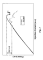
- Fig. 2 illustrates the improvement achieved by adding CIG elements according to the invention to the RWG laser diode structure.
- the figure shows the P-I curve, i.e. power versus injected current in arbitrary units (a.u.), for a standard diode compared to a CIG-improved diode.
- Indicated is the first occurring kink, i.e. instability of the optical output power of a standard diode vs. a CIG-improved diode.
- the first kink clearly occurs at a much lower power level for the standard diode than for the same diode comprising CIG elements.
- stable output powers of more than 900 mW were achieved with the improved CIG design with good life test results.
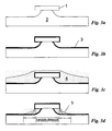
- Fig. 3a starts with the ridge formation by a wet etching process.
- the part of a semiconductor body 2 which is supposed to form the ridge of the final RWG laser diode is covered by a photoresist mask 1, the ridge etching mask.
- GaAs or AlGaAs are the preferred materials for the body 2.
- the etching step results in a semiconductor body 2 having the shape shown in Fig. 3a, i.e. the ridge is formed.
- the shape results from a wet etching process, but the CIG element formation process will work as well on other ridge shapes having, e.g. straight side walls or sidewalls of other shapes.
- Important for the later described CIG layer self-aligned masking process is only the presence of some kind of a mesa structure.
- the deposition can be achieved by a PECVD process, i.e. by Physically Enhanced Chemical Vapor Deposition.
- the thickness of this insulator layer 3 is in the region of 200 to 300 nm, preferably about 220 nm.
- the insulator layer 3 can also be made of alternative materials, such as SiO 2 , AIN, or TiO 2 , and be deposited by alternative deposition methods, such as PVD, i.e. Physical Vapor Deposition, or CVD, i.e. Chemical Vapour Deposition.
- Figs. 3c to 3g produce the mask that defines the location of the absorbing CIG elements. It is effectively the thick Si 3 N 4 insulator layer 3 that acts as a mask for the desired absorbing layer. This insulator layer optically separates the light generated in the waveguide from the absorbing layer. In the regions with thick Si 3 N 4 , any absorbing layer deposited on top will not (or only marginally) contribute to the absorption.
- a photoresist layer 4 is deposited over the whole semiconductor body 2, including insulator layer 3 and mask 1.
- the photoresist is spun over the semiconductor body 2, resulting in a thicker photoresist layer near the ridge and a thinner photoresist layer in the body region.
- the thickness of the resulting photoresist layer 4 is preferably about 2.5 ⁇ m in the region of the ridge and about 1 ⁇ m in the body region.
- the thickness gradient of the photoresist layer 4 is important for the variability of the absorbing layer (or CIG element) location and shape, as will be shown later.
- the photoresist deposition of Fig. 3c prepares the device for the subsequent Si 3 N 4 masking.
- the photoresist is etched to a desired shape, here specifically a variable width or distance, measured from the ridge center.
- a preferred method for this shaping step is RIE, i.e. Reactive Ion Etching. This results in the shaping masks 5 illustrated in Fig. 3d.
- the control of the width of this shaping mask may be facilitated by a rather directional etching process and/or the choice of an appropriate etch time. A person skilled in the art will know how to modify the etching process in order to achieve the desired result.
- Fig. 3d shows three different masks: a narrow one, essentially of the same width as the ridge etching photoresist mask 1; a middle one, somewhat wider than said ridge etching mask 1; and a wide one, identified by the outermost line shown in Fig. 3d. All three widths are shown to clearly demonstrate the variability of the mask.
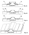
- the insulator layer 3 established earlier as described above with Fig. 3b, is etched down to the semiconductor body 2.
- the insulator layer 3 remains only at the flanks of the ridge and underneath the photoresist mask which was established in the previous step (Fig. 3d) and forms the insulator strips 6a and 6b on both sides of the ridge. They extend preferably along the whole length of the semiconductor body 2, but may be shorter than the latter if desired.
- the total width of the insulator strips 6a and 6b varies with the width of the shaping mask 5.
- the shape of the insulator strips also determines the effective location of the CIG element, i.e. the location where absorption of light mainly occurs.
- the photoresist shaping mask 5 used for the Si 3 N 4 or any similar etching as well as the ridge etching photoresist mask 1 are removed, e.g. by lift-off.
- the result is illustrated in Fig. 3f.
- a layer of optically absorbing material resulting in an uninterupted layer covering the whole semiconductor body 2 is deposited.
- This layer has two functions :
- this absorption layer must have two important material properties:
- Fig. 3h shows the nearly complete RWG laser diode structure having the additional P-contact layers 9 deposited necessary for electrical powering of the diode.
- Fig. 3i finally shows, somewhat similar to Fig. 1, the optical power distribution of the RWG laser diode shown in Fig. 3h approximately in relative dimensions to the structure in Fig. 3h. It is clearly visible that the fundamental mode has its usual peak in the center of the laser diode, whereas the first order mode - as any higher order modes - extend further into the areas where the CIG elements are located. Thus, the first and higher modes are strongly attenuated, which is what the invention intends to achieve.
- the lateral extension of the modes within the laser diode varies. Accordingly, changes must be made with regard to the optimal location of the CIG elements to achieve the desired maximum absorption of first and higher order modes and minimum absorption of the fundamental mode. It is therefore important to have a process that allows variable placement and shape of the CIG elements independent of, but adapted to, the laser's ridge shape and design.
- the present invention provides this flexiblity and adaptibility.
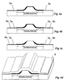
- Figs. 4a to 4d show a first alternative starting after the formation step of mask 5 in Fig. 3d.
- the thick insulator layer 3 established earlier as explained above with Fig. 3b, is not etched down to the semiconductor body 2, but to a predetermined thickness on the body. This etching results in relatively thin insulating layers 7a and 7b, as shown in Fig. 4a, extending over the whole of or part of the semiconductor body.
- Their thickness may be selected in the region of 15 to 40 nm, preferably about 25. The choice depends on the desired overall absorption of the CIG element.
- the insulator strips 6a and 6b and/or the thin outer insulator layers 7a and 7b extend preferably along the whole length and width of the semiconductor body, but may also be shorter and/or narrower than the latter if desired.
- the thin outer insulator layers 7a and 7b electrically separate the absorbing material from the semiconductor and thus avoid any undesired leak currents and/or undesired material interactions at the interface. Furthermore, they may be utilized to modify the overall absorption of the CIG element.
- Fig. 4b shows the structure after lift-off of the photoresist masks 1 and 5, as previously described for Fig. 3f.
- the next step is the deposition of the absorbing layer 8a and 8b as part of the p-metallisation.
- the result is demonstrated in Fig. 4c and was previously described for Fig. 3g.
- Fig. 4d shows the nearly complete RWG laser diode structure having the additional P-contact layer 9 deposited necessary for electrical powering of the diode.
- the CIG elements located left and right of the ridge now consist of two layers: the thin insulating layers 7a and 7b and the optically absorbing layers 8a and 8b.
- Figs. 5a to 5d show a second alternative for fabricating a CIG element with an insulation layer underneath the absorbing layer.
- the thick insulating layer is etched down to the semiconductor body 2.
- the photoresist masks are subsequently removed by lift-off to result in a structure containing the semiconductor body 2 with the ridge and the two thick insulating layers 6a and 6b to both sides of the ridge. This is shown in Fig. 5a.
- a thin insulating layer again preferably 25 nm, is deposited covering the entire semiconductor body 2, thus forming the first layer of the CIG elements 7a and 7b as shown in Fig. 5b.
- the material can now be choosen and deposited independent of the thick insulating material. Standard materials and deposition methods for this purpose are insulators such as Si 3 N 4 , TiO 2 , SiO 2 , AIN deposited by PVD, CVD or MOCVD.
- this thin insulator covers the entire surface of the semiconductor body, it also covers the contact area on top of the ridge. In this latter area, the thin insulator must be removed to provide electrical contact of the semiconductor with the p-metal. This can be done by any common method with photoresist masks and subsequent etching, preferably RIE etching. A person skilled in the art will know how to realize this. The result is shown in Fig. 5c.
- the p-metal layer 9 which also provides and functions as the absorption layers 8a and 8b of the CIG element, is deposited resulting in a structure shown in Fig. 5d.
- Fig. 6a shows the structure with the thick insulating layers 6a and 6b at both sides of the ridge and the thin insulating layer 7a/b deposited across the entire semiconductor surface. This structure is generated in the same manner as described earlier for Fig. 5b.
- an absorption layer is deposited, also covering the entire body and forming the necessary absorption layers 8a and 8b for the CIG elements. This is shown in Fig. 6b.
- the two layers forming the CIG element 7a/b and 8a/b must be removed from the p-contact area. This is again done by any common masking and subsequent etching step and results in the structure shown in Fig. 6c.
- Fig. 6d finally shows the RWG structure after deposition of the p-metallisation, i.e. the p-contact layer 9.
- the advantage of the process described last is the ability to choose any stack of materials for the CIG element composition independent of p-metallisation.
- the only requirement for the absorption layer 8a/b remains now the absorption property at the lasing wavelength.
- the choice of materials was limited to materials providing good contact to the semiconductor, preferably a conductor of the type Ti, Cr, Pt.
- any material and thickness can be used as long as the material provides absorption at the lasing wavelength.
- the CIG element can be modified to any shape to cover only part of the semiconductor body.
- FIGs. 7a to 7c A fourth alternative is described in Figs. 7a to 7c.
- an absorption layer 8a, 8b is deposited over the semiconductor body 2, including both the ridge etching mask 1 and the photoresist shaping masks 5. This is shown in Fig. 7a.
- CIG elements 8a and 8b remain, extending over the semiconductor body except the ridge and its vicinity, i.e. the insulator strips 6a, 6b and 7a, 7b.
- the result, shown in Fig. 7b are two separate CIG elements 8a and 8b.
- the absorption layer may extend over only part of the semiconductor body. A person skilled in the art will know how to achieve this.
- Fig. 7c shows the structure after lifting-off the masks and depositing the usual P-contact metallisation layer 9.
- the advantage of this alternative is that material and thickness for the P-contact metallisation and the CIG element can be chosen independently.
Landscapes
- Physics & Mathematics (AREA)
- Condensed Matter Physics & Semiconductors (AREA)
- General Physics & Mathematics (AREA)
- Electromagnetism (AREA)
- Optics & Photonics (AREA)
- Geometry (AREA)
- Semiconductor Lasers (AREA)
Claims (23)
- Laserdiode mit einem Halbleitersubstrat (2) und einem aktiven Bereich, der einen Steghohlleiter enthält, wobei die Laserdiode ein Licht absorbierendes Element zur Unterdrückung von Wellenformen erster und höherer Ordnung hat, dadurch gekennzeichnet, dass
das absorbierende Element aus einem oder mehreren komplexen Indexführungselementen (CIG-Element) mit mindestens einer Absorptionsschicht (8a, 8b) und einer Isolationsschicht besteht bzw. sie enthält, wobei sich die Isolationsschicht (3) zwischen dem Halbleitersubstrat (2) und der Absorptionsschicht (8a, 8b) befindet,
und das eine CIG-Element bzw. die mehreren CIG-Elemente an einem vorbestimmten Platz auf dem Halbleitersubstrat (2) entlang des und parallel zum Steghohlleiter angeordnet ist bzw. sind, wobei Platz, Anzahl und Struktur der CIG-Elemente so ausgewählt sind, dass die Unterdrückung unerwünschter Moden höherer Ordnung der Laserdiode durch die Isolationsschicht (3) maximiert wird, die entwederlaterale Sektionen unterschiedlicher Dicke aufweist, wobei eine erste Sektion in der Nähe des Steghohlleiters eine größere Dicke (6a, 6b) und eine zweite Sektion in einiger Entfernung von dem Steghohlleiter eine geringere Dicke (7a, 7b) aufweist,oder eine laterale Ausdehnung aufweist, die kleiner als die Absorptionsschicht (8a, 8b) ist. - Laserdiode nach Anspruch 1, dadurch gekennzeichnet, dass
zwei oder mehrere CIG-Elemente symmetrisch an einem vorbestimmten Platz auf dem Halbleitersubstrat angeordnet sind. - Laserdiode nach Anspruch 1, dadurch gekennzeichnet, dass
die Absorptionsschicht (8a, 8b) weiterhin als Kontaktschicht für den Steghohlleiter des Lasers dient. - Laserdiode nach Anspruch 1, dadurch gekennzeichnet, dass
das CIG-Element oder die CIG-Elemente aus einer Mehrzahl oder einem Stapel von Isolations- und Absorptionsschichten (8a, 8b) besteht bzw. bestehen oder umfasst bzw. umfassen. - Laserdiode nach einem der vorangehenden Ansprüche, dadurch gekennzeichnet, dass
mindestens zwei CIG-Elemente als Schichtstrukturen vorgesehen sind, die sich vorzugsweise auf beiden Seiten des Steghohlleiters befinden und sich über die gesamte Länge des Halbleitersubstrats (2) erstrecken. - Laserdiode nach einem der Ansprüche 1 bis 4, dadurch gekennzeichnet, dass mindestens zwei CIG-Elemente als Schichtstrukturen vorgesehen sind, wobei je eine sich vorzugsweise auf beiden Seiten des Steghohlleiters befindet und sich nur teilweise entlang der Länge des Halbleitersubstrats (2) erstreckt.
- Laserdiode nach Anspruch 1, dadurch gekennzeichnet, dass
das CIG-Element so gestaltet ist, dass es die Unterdrückung von Moden erster und höherer Ordnung maximiert und gleichzeitig die Absorption der Grundmode minimiert. - Laserdiode nach einem der vorangehenden Ansprüche, dadurch gekennzeichnet, dass
die Dicke der Isolationsschicht zwischen dem Halbleitersubstrat (2) und der Absorptionsschicht (8a, 8b) so ausgewählt wird, dass die Absorption der Grundmode minimiert und gleichzeitig die Unterdrückung der Moden erster und höherer Ordnung maximiert wird. - Laserdiode nach einem der vorangehenden Ansprüche, dadurch gekennzeichnet, dass
die Dicke der Absorptionsschicht (8a, 8b) so ausgewählt wird, dass die Unterdrückung der Moden erster und höherer Ordnung maximiert und gleichzeitig die Absorption der Grundmode minimiert wird. - Laserdiode nach einem der vorangehenden Ansprüche, dadurch gekennzeichnet, dass
das Material der Absorptionsschicht (8a, 8b) so ausgewählt wird, dass die Unterdrückung der Moden erster und höherer Ordnung maximiert und gleichzeitig die Absorption der Grundmode minimiert wird. - Laserdiode nach Anspruch 4, dadurch gekennzeichnet, dass
die Materialien und Dicke für das CIG-Element oder -Elemente so ausgewählt werden, dass die Unterdrückung der Moden erster und höherer Ordnung maximiert und gleichzeitig die Absorption der Grundmode minimiert wird. - Laserdiode nach einem der vorangehenden Ansprüche, dadurch gekennzeichnet, dass
die Absorptionsschicht (8a, 8b) einen Teil des Halbleitersubstrats bedeckt, vorzugsweise die gesamte Oberfläche des Substrats. - Laserdiode nach Anspruch 12, dadurch gekennzeichnet, dass
die Absorptionsschicht (8a, 8b) weiterhin als Kontaktschicht für den Steghohlleiter des Lasers dient. - Laserdiode nach einem der vorangehenden Ansprüche, dadurch gekennzeichnet, dass
das Halbleitersubstrat (2) aus Materialien auf der Basis von zum Beispiel GaAs oder InP besteht und das komplexe Indexführungselement einen Leiter oder Halbleiter umfasst, zum Beispiel Ti, Cr, Pt, Au, Si. - Laserdiode nach einem der vorangehenden Ansprüche, dadurch gekennzeichnet, dass
das Halbleitersubstrat aus Materialien auf der Basis von zum Beispiel GaAs oder InP besteht und das komplexe Indexführungselement einen Isolator umfasst, zum Beispiel TiO2, Si3N4, AIN, SiO2. - Verfahren zur Herstellung einer Hochleistungs-Laserdiode mit einem Halbleitersubstrat (2) und einem Steghohlleiter als aktiven Bereich, das die folgenden Verfahrensschritte umfasst:(a) Bereitstellen des Halbleitersubstrats mit dem Steghohlleiter durch eine erste Fotolackmaske (Fig. 3a, 1),(b) Auftragen eines Isolators (Fig. 3b, 3) auf mindestens einen Teil des Halbleitersubstrats, einschließlich der ersten Maske (1),(c) Auftragen eines Fotolacks (Fig. 3c, 4) auf den Isolator,(d) Entfernen eines Teils des Fotolacks auf kontrollierte Weise um eine zweite Fotolackmaske (Fig. 3d, 5) mit einer vorbestimmten Größe zu schaffen, die breiter als der Steghohlleiter ist,(e) Entfernen des Isolators (Fig. 3e) an der Stelle, wo er durch die zweite Maske nicht bedeckt ist,(f) Entfernen sowohl der ersten als auch der zweiten Fotolackmaske (Fig. 3f),(g) Auftragen einer Absorptionsschicht (Fig. 3g, 8a, 8b) als Teil eines komplexen Indexführungselementes (CIG) und als Kontaktschicht (Fig. 3h, 9).
- Verfahren nach Anspruch 16, dadurch gekennzeichnet, dass
der Verfahrensschritt (e) durch (e') ersetzt wird:Verdünnen des Isolators (Fig. 4b) auf eine vorbestimmte Dicke an der Stelle, wo er durch die zweite Maske nicht bedeckt ist, um Isolatorbereiche mit einer ersten Dicke (6a, 6b) unter der zweiten Maske und mit einer zweiten Dicke (7a, 7b) außerhalb der zweiten Maske zu schaffen. - Verfahren nach Anspruch 16 oder 17, dadurch gekennzeichnet, dass
der Verfahrensschritt (g) durch die Verfahrensschritte (g') und (g") ersetzt wird:(g') Auftragen einer Absorptionsschicht (Fig. 3g, 8a, 8b) als Teil eines komplexen Indexführungselementes (CIG) und(g") Auftragen einer Kontaktschicht (Fig. 3h, 9). - Verfahren zur Herstellung einer Hochleistungs-Laserdiode mit einem Halbleitersubstrat (2) und einem Steghohlleiter als aktiven Bereich, das die folgenden Verfahrensschritte umfasst:(a) Herstellung des Steghohlleiters auf dem Halbleitersubstrat mit Hilfe einer ersten Fotolackmaske (Fig. 3a, 1),(b) Auftragen eines Isolators (Fig. 3b, 3) auf zumindest einen Teil des Halbleitersubstrats (2) einschließlich der ersten Maske (1),(c) Auftragen eines Fotolacks (Fig. 3c, 4) auf den Isolator (3),(d) Entfernen eines Teils des Fotolacks (Fig. 3d) auf gesteuerte Weise, um eine zweite Fotolackmaske (5) mit einer vorbestimmten Größe zu schaffen, die breiter als der Steghohlleiter ist,(e) Entfernen des Isolators (Fig. 3e) an der Stelle, wo er durch die zweite Maske (5) nicht bedeckt ist,(f) Entfernen sowohl der ersten als auch der zweiten Fotolackmaske (1, 5), einschließlich eines Teils des Isolators (3),(g) Auftragen eines dünnen Isolators (Fig. 5b, 7a, 7b) auf zumindest einen Teil des Halbleitersubstrats einschließlich des Steghohlleiters,(h) Entfernen des dünnen Isolators im Kontaktbereich des Steghohlleiters (Fig. 5c),(i) Auftragen einer Absorptionsschicht (Fig. 5d, 8a, 8b) als Teil eines komplexen Indexführungselementes (CIG) und als Kontaktschicht (Fig. 5d, 9).
- Verfahren nach Anspruch 19, dadurch gekennzeichnet, dass
der Verfahrensschritt (i) durch die Verfahrensschritte (i') und (i") ersetzt wird:(i') Auftragen einer Absorptionsschicht (Fig. 3g, 8a, 8b) als Teil eines komplexen Indexführungselementes (CIG) und(i") Auftragen einer Kontaktschicht (Fig. 3h, 9). - Verfahren nach Anspruch 20, dadurch gekennzeichnet, dass
der Verfahrensschritt (g) durch (g') ersetzt wird:Auftragen eines dünnen Isolators und einer Absorptionsschicht auf zumindest einen Teil des Halbleitersubstrats, einschließlich des Steghohlleiters,und Verfahrensschritt (h) durch (h') ersetzt wird:Entfernen des dünnen Isolators und der Absorptionsschicht im Kontaktbereich des Steghohlleiters, wobei der dünne Isolator und die Absorptionsschicht (8a, 8b) als CIG-Elemente auf beiden Seiten des Steghohlleiters belassen werden. - Verfahren nach Anspruch 21, dadurch gekennzeichnet, dass
der Verfahrensschritt (g') durch (g") ersetzt wird:Auftragen eines Stapels von Isolatoren und Absorptionsschichten auf zumindest einen Teil des Halbleitersubstrats, einschließlich des Steghohlleiters,und Verfahrensschritt (h') durch (h") ersetzt wird:Entfernen des Stapels im Kontaktbereich des Steghohlleiters, wobei der Stapel als CIG-Elemente auf beiden Seiten des Steghohlleiters belassen wird. - Verfahren nach einem der Ansprüche 16 bis 22, dadurch gekennzeichnet, dass
der aufgetragene Isolator Si3N4, SiO2, TiO2 und/oder AIN ist und das leitfähige Material für die Absorptions- und/oder Kontaktschichten Au, Cr, Pt und/oder Ti ist.
Applications Claiming Priority (3)
| Application Number | Priority Date | Filing Date | Title |
|---|---|---|---|
| US245199 | 1981-03-18 | ||
| US10/245,199 US6862300B1 (en) | 2002-09-17 | 2002-09-17 | High power semiconductor laser diode and method for making such a diode |
| PCT/IB2003/003929 WO2004027951A1 (en) | 2002-09-17 | 2003-08-22 | High power semiconductor laser diode and method for making such a diode |
Publications (2)
| Publication Number | Publication Date |
|---|---|
| EP1547216A1 EP1547216A1 (de) | 2005-06-29 |
| EP1547216B1 true EP1547216B1 (de) | 2007-02-14 |
Family
ID=32028932
Family Applications (1)
| Application Number | Title | Priority Date | Filing Date |
|---|---|---|---|
| EP03797442A Expired - Lifetime EP1547216B1 (de) | 2002-09-17 | 2003-08-22 | Hochleistungs-halbleiterlaserdiode und verfahren zur herstellung einer solchen diode |
Country Status (5)
| Country | Link |
|---|---|
| US (3) | US6862300B1 (de) |
| EP (1) | EP1547216B1 (de) |
| AU (1) | AU2003263419A1 (de) |
| DE (1) | DE60311844T2 (de) |
| WO (1) | WO2004027951A1 (de) |
Families Citing this family (12)
| Publication number | Priority date | Publication date | Assignee | Title |
|---|---|---|---|---|
| DE102006046297A1 (de) * | 2006-09-29 | 2008-04-03 | Osram Opto Semiconductors Gmbh | Halbleiterlaser |
| US8073031B2 (en) * | 2008-03-03 | 2011-12-06 | Sharp Kabushiki Kaisha | Laser diode with improved heat dissipation |
| US20100248715A1 (en) * | 2009-03-31 | 2010-09-30 | Soren Lundsgaard | Systems and method for optimizing wireless local area network channel scanning |
| US9268089B2 (en) * | 2011-04-21 | 2016-02-23 | Octrolix Bv | Layer having a non-linear taper and method of fabrication |
| US8718432B1 (en) * | 2011-04-21 | 2014-05-06 | Octrolix Bv | Method for forming a spotsize converter |
| DE102011075502A1 (de) | 2011-05-09 | 2012-11-15 | Forschungsverbund Berlin E.V. | Breitstreifen-Diodenlaser mit hoher Effizienz und geringer Fernfelddivergenz |
| WO2015002683A2 (en) | 2013-04-09 | 2015-01-08 | Nlight Photonics Corporation | Diode laser packages with flared laser oscillator waveguides |
| US9166369B2 (en) | 2013-04-09 | 2015-10-20 | Nlight Photonics Corporation | Flared laser oscillator waveguide |
| US10186836B2 (en) | 2014-10-10 | 2019-01-22 | Nlight, Inc. | Multiple flared laser oscillator waveguide |
| WO2016197137A1 (en) | 2015-06-04 | 2016-12-08 | Nlight, Inc. | Angled dbr-grating laser/amplifier with one or more mode-hopping regions |
| WO2018081602A2 (en) * | 2016-10-28 | 2018-05-03 | Nlight, Inc. | Method, system and apparatus for higher order mode suppression |
| US11031753B1 (en) * | 2017-11-13 | 2021-06-08 | The Government Of The United States Of America As Represented By The Secretary Of The Air Force | Extracting the fundamental mode in broad area quantum cascade lasers |
Family Cites Families (10)
| Publication number | Priority date | Publication date | Assignee | Title |
|---|---|---|---|---|
| US4227975A (en) * | 1979-01-29 | 1980-10-14 | Bell Telephone Laboratories, Incorporated | Selective plasma etching of dielectric masks in the presence of native oxides of group III-V compound semiconductors |
| JPS5726488A (en) | 1980-07-23 | 1982-02-12 | Fujitsu Ltd | Semiconductor light emitting device |
| JPS6261385A (ja) | 1985-09-11 | 1987-03-18 | Sharp Corp | 半導体レ−ザ−素子 |
| JPS62270170A (ja) | 1986-05-20 | 1987-11-24 | 住友ベークライト株式会社 | 呼吸同調式酸素供給装置 |
| NL8603009A (nl) * | 1986-11-27 | 1988-06-16 | Philips Nv | Halfgeleiderlaser en werkwijze ter vervaardiging daarvan. |
| JPH0334595A (ja) * | 1989-06-30 | 1991-02-14 | Matsushita Electric Ind Co Ltd | 半導体レーザ及びその製造方法 |
| JPH0521902A (ja) | 1991-07-11 | 1993-01-29 | Mitsubishi Electric Corp | 半導体レーザ装置 |
| JP3649207B2 (ja) | 1995-09-20 | 2005-05-18 | 三菱マテリアル株式会社 | 単結晶四ほう酸リチウムの製造方法 |
| US6141365A (en) * | 1997-12-31 | 2000-10-31 | Lasertron | Semiconductor laser with kink suppression layer |
| JP3849758B2 (ja) * | 2001-04-12 | 2006-11-22 | ソニー株式会社 | 半導体レーザ素子 |
-
2002
- 2002-09-17 US US10/245,199 patent/US6862300B1/en not_active Expired - Lifetime
-
2003
- 2003-08-22 DE DE60311844T patent/DE60311844T2/de not_active Expired - Fee Related
- 2003-08-22 EP EP03797442A patent/EP1547216B1/de not_active Expired - Lifetime
- 2003-08-22 AU AU2003263419A patent/AU2003263419A1/en not_active Abandoned
- 2003-08-22 WO PCT/IB2003/003929 patent/WO2004027951A1/en not_active Ceased
-
2005
- 2005-01-21 US US11/040,246 patent/US20050201438A1/en not_active Abandoned
-
2008
- 2008-01-10 US US11/972,156 patent/US7623555B2/en not_active Expired - Lifetime
Also Published As
| Publication number | Publication date |
|---|---|
| WO2004027951A1 (en) | 2004-04-01 |
| US20050201438A1 (en) | 2005-09-15 |
| AU2003263419A1 (en) | 2004-04-08 |
| EP1547216A1 (de) | 2005-06-29 |
| US7623555B2 (en) | 2009-11-24 |
| DE60311844T2 (de) | 2007-12-13 |
| US6862300B1 (en) | 2005-03-01 |
| US20080123697A1 (en) | 2008-05-29 |
| DE60311844D1 (de) | 2007-03-29 |
Similar Documents
| Publication | Publication Date | Title |
|---|---|---|
| US7623555B2 (en) | High power semiconductor laser diode | |
| US5317587A (en) | VCSEL with separate control of current distribution and optical mode | |
| KR101532982B1 (ko) | 레이저 광원 | |
| JP6490705B2 (ja) | 半導体光集積素子およびその製造方法 | |
| US6852558B2 (en) | Methods for forming index guided vertical cavity surface emitting lasers | |
| US8319229B2 (en) | Optical semiconductor device and method for manufacturing the same | |
| US6366595B1 (en) | Semiconductor laser with kink suppression layer | |
| CN101123342B (zh) | 光波导、半导体光学集成元件及其制造方法 | |
| US20110091147A1 (en) | Integrated semiconductor optical device | |
| CN101390263B (zh) | 半导体激光装置 | |
| EP0527615B1 (de) | Verfahren zur Herstellung eines abstimmbaren Halbleiterlasers | |
| US20110091151A1 (en) | Integrated semiconductor optical device | |
| JP2012089622A (ja) | 半導体レーザ素子 | |
| CN111969415B (zh) | 一种宽谱多波长法布里-珀罗激光器 | |
| KR20150139694A (ko) | 분포 브래그 반사기 리지 레이저 다이오드 및 이의 제조 방법 | |
| KR100413527B1 (ko) | 단일 집적 반도체 광소자 제작방법 | |
| KR20060038057A (ko) | 반도체 레이저 소자 및 그 제조 방법 | |
| EP1504506A2 (de) | Halbleiterlaser | |
| US6316280B1 (en) | Method of manufacturing semiconductor devices separated from a wafer | |
| JP2021153125A (ja) | 量子カスケードレーザ | |
| WO2008114896A1 (en) | High power single mode optical devices with s-bending ridge waveguide and fabrication method thereof | |
| JP2002057409A (ja) | 半導体レーザ及びその製造方法 | |
| WO2002063731A2 (en) | Sampled grating distributed reflector laser | |
| JP3788699B2 (ja) | 集積型光回路素子及びその製造方法 | |
| JP2013524527A (ja) | 半導体レーザーダイオード |
Legal Events
| Date | Code | Title | Description |
|---|---|---|---|
| PUAI | Public reference made under article 153(3) epc to a published international application that has entered the european phase |
Free format text: ORIGINAL CODE: 0009012 |
|
| 17P | Request for examination filed |
Effective date: 20050418 |
|
| AK | Designated contracting states |
Kind code of ref document: A1 Designated state(s): AT BE BG CH CY CZ DE DK EE ES FI FR GB GR HU IE IT LI LU MC NL PT RO SE SI SK TR |
|
| AX | Request for extension of the european patent |
Extension state: AL LT LV MK |
|
| DAX | Request for extension of the european patent (deleted) | ||
| RBV | Designated contracting states (corrected) |
Designated state(s): DE FR GB |
|
| RAP1 | Party data changed (applicant data changed or rights of an application transferred) |
Owner name: BOOKHAM TECHNOLOGY PLC |
|
| GRAP | Despatch of communication of intention to grant a patent |
Free format text: ORIGINAL CODE: EPIDOSNIGR1 |
|
| GRAS | Grant fee paid |
Free format text: ORIGINAL CODE: EPIDOSNIGR3 |
|
| GRAA | (expected) grant |
Free format text: ORIGINAL CODE: 0009210 |
|
| AK | Designated contracting states |
Kind code of ref document: B1 Designated state(s): DE FR GB |
|
| REG | Reference to a national code |
Ref country code: GB Ref legal event code: FG4D |
|
| REF | Corresponds to: |
Ref document number: 60311844 Country of ref document: DE Date of ref document: 20070329 Kind code of ref document: P |
|
| EN | Fr: translation not filed | ||
| PLBE | No opposition filed within time limit |
Free format text: ORIGINAL CODE: 0009261 |
|
| STAA | Information on the status of an ep patent application or granted ep patent |
Free format text: STATUS: NO OPPOSITION FILED WITHIN TIME LIMIT |
|
| 26N | No opposition filed |
Effective date: 20071115 |
|
| GBPC | Gb: european patent ceased through non-payment of renewal fee |
Effective date: 20070822 |
|
| PG25 | Lapsed in a contracting state [announced via postgrant information from national office to epo] |
Ref country code: FR Free format text: LAPSE BECAUSE OF FAILURE TO SUBMIT A TRANSLATION OF THE DESCRIPTION OR TO PAY THE FEE WITHIN THE PRESCRIBED TIME-LIMIT Effective date: 20071005 |
|
| PG25 | Lapsed in a contracting state [announced via postgrant information from national office to epo] |
Ref country code: DE Free format text: LAPSE BECAUSE OF NON-PAYMENT OF DUE FEES Effective date: 20080301 |
|
| PG25 | Lapsed in a contracting state [announced via postgrant information from national office to epo] |
Ref country code: FR Free format text: LAPSE BECAUSE OF FAILURE TO SUBMIT A TRANSLATION OF THE DESCRIPTION OR TO PAY THE FEE WITHIN THE PRESCRIBED TIME-LIMIT Effective date: 20070214 Ref country code: GB Free format text: LAPSE BECAUSE OF NON-PAYMENT OF DUE FEES Effective date: 20070822 |