EP1544894A2 - Verfahren und Vorrichtung zur Aberrationskorrektur in Ladungsträgerteilchenstrahlen - Google Patents
Verfahren und Vorrichtung zur Aberrationskorrektur in Ladungsträgerteilchenstrahlen Download PDFInfo
- Publication number
- EP1544894A2 EP1544894A2 EP04257912A EP04257912A EP1544894A2 EP 1544894 A2 EP1544894 A2 EP 1544894A2 EP 04257912 A EP04257912 A EP 04257912A EP 04257912 A EP04257912 A EP 04257912A EP 1544894 A2 EP1544894 A2 EP 1544894A2
- Authority
- EP
- European Patent Office
- Prior art keywords
- aberrations
- profile
- charged
- probe
- aberration
- Prior art date
- Legal status (The legal status is an assumption and is not a legal conclusion. Google has not performed a legal analysis and makes no representation as to the accuracy of the status listed.)
- Withdrawn
Links
- 230000004075 alteration Effects 0.000 title claims abstract description 164
- 238000000034 method Methods 0.000 title claims abstract description 30
- 239000002245 particle Substances 0.000 title claims abstract description 30
- 239000000523 sample Substances 0.000 claims abstract description 65
- 238000012937 correction Methods 0.000 claims abstract description 52
- 238000004364 calculation method Methods 0.000 claims abstract description 6
- 238000000605 extraction Methods 0.000 claims abstract description 5
- 239000000284 extract Substances 0.000 abstract description 6
- 230000005405 multipole Effects 0.000 description 34
- 239000011159 matrix material Substances 0.000 description 12
- 238000010894 electron beam technology Methods 0.000 description 7
- 230000005684 electric field Effects 0.000 description 5
- 230000005284 excitation Effects 0.000 description 5
- 238000013461 design Methods 0.000 description 4
- 238000010586 diagram Methods 0.000 description 4
- 230000005484 gravity Effects 0.000 description 4
- 230000003287 optical effect Effects 0.000 description 3
- 238000012545 processing Methods 0.000 description 3
- 238000011002 quantification Methods 0.000 description 3
- 230000009471 action Effects 0.000 description 2
- 230000003213 activating effect Effects 0.000 description 2
- 230000008901 benefit Effects 0.000 description 2
- 230000004913 activation Effects 0.000 description 1
- 230000005540 biological transmission Effects 0.000 description 1
- 238000002474 experimental method Methods 0.000 description 1
- 230000006870 function Effects 0.000 description 1
- 238000003384 imaging method Methods 0.000 description 1
- 230000006872 improvement Effects 0.000 description 1
- 239000000696 magnetic material Substances 0.000 description 1
- MYWUZJCMWCOHBA-VIFPVBQESA-N methamphetamine Chemical compound CN[C@@H](C)CC1=CC=CC=C1 MYWUZJCMWCOHBA-VIFPVBQESA-N 0.000 description 1
- 230000002093 peripheral effect Effects 0.000 description 1
- 230000004044 response Effects 0.000 description 1
- 238000004088 simulation Methods 0.000 description 1
Images

Classifications
-
- H—ELECTRICITY
- H01—ELECTRIC ELEMENTS
- H01J—ELECTRIC DISCHARGE TUBES OR DISCHARGE LAMPS
- H01J37/00—Discharge tubes with provision for introducing objects or material to be exposed to the discharge, e.g. for the purpose of examination or processing thereof
- H01J37/02—Details
- H01J37/04—Arrangements of electrodes and associated parts for generating or controlling the discharge, e.g. electron-optical arrangement or ion-optical arrangement
- H01J37/153—Electron-optical or ion-optical arrangements for the correction of image defects, e.g. stigmators
-
- H—ELECTRICITY
- H01—ELECTRIC ELEMENTS
- H01J—ELECTRIC DISCHARGE TUBES OR DISCHARGE LAMPS
- H01J37/00—Discharge tubes with provision for introducing objects or material to be exposed to the discharge, e.g. for the purpose of examination or processing thereof
- H01J37/26—Electron or ion microscopes; Electron or ion diffraction tubes
- H01J37/28—Electron or ion microscopes; Electron or ion diffraction tubes with scanning beams
Definitions
- the present invention relates to a method of automatically correcting aberrations in a charged-particle beam and to an apparatus therefor.
- an aberration corrector is built in the electron optical system to permit high-resolution imaging and to enhance the probe current density.
- a system consisting of an aberration corrector having four stages of multipole units is proposed as the first-mentioned built-in aberration corrector.
- Each multipole unit has 12 pole elements.
- Chromatic aberration is corrected by a combination of an electrostatic quadrupole mode of operation and a magnetic quadrupole mode of operation.
- Spherical aberration is corrected by four stages of octopole mode of operation. The principle is introduced in detail in Non-Patent References 1 to 3.
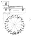
- an aberration corrector C is disposed ahead of an objective lens 7 and equipped with four stages of multipole units 51, 52, 53, and 54.
- Each of the multipole units 51-54 has 12 pole elements.
- Electric potentials 1, 2, 3, and 4 are applied to the multipole elements 51-54, respectively, to activate the electrostatic quadrupole elements.
- Exciting currents 5 and 6 are supplied to the second and third stages of multipole units 52 and 53, respectively, to produce magnetic potential distribution analogous to the electric potential distribution created by the potentials 2 and 3 and to produce a magnetic field superimposed on the electric field.
- electric potentials 11, 12, 13, and 14 are applied to the multipole units 51-54, respectively, to activate an electrostatic octopole element for producing an electric field superimposed on the electric field produced by the potentials 1-4 that are used to activate the quadrupole.
- a reference orbit for the beam B is created by the four stages of multipole units 51-54 and objective lens 7.
- the beam B is focused onto a specimen surface 20.
- X-direction orbit R x and Y-direction orbit R y of the beam B are both schematically drawn on the same plane.
- the reference orbit can be understood as a paraxial orbit that is assumed when there is no aberration. That is, the Y-direction orbit R y is made to pass through the center of the multipole unit 52 by the multipole unit 51. The X-direction orbit R x is made to pass through the center of the multipole unit 53 by the multipole unit 52. Finally, the charged-particle beam B is focused onto the specimen surface 20 by the multipole units 53, 54 and objective lens 7. In practice, these need to be adjusted mutually for complete focusing. At this time, the dipole-activating potentials applied to the four stages of multipole units 51-54 are used for axial alignment.
- the charged-particle beam B in the X-direction orbit R x is diffused by the multipole unit 51 acting like a concave lens. Then, the beam is focused by the multipole unit 52 acting like a convex lens and made to pass through the center of the multipole unit 53. Then, the beam is focused by the multipole unit 54 and moves toward the objective lens 7.
- the beam B in the Y-direction orbit R y is focused by the multipole unit 51 and made to pass through the center of the multipole unit 52. Then, the beam is focused by the multipole unit 53. Finally, the beam is diffused by the multipole unit 54 and moves toward the objective lens 7.
- the electron optical system can be operated like a single concave or convex lens.
- Spherical aberration is corrected after X- and Y-direction chromatic aberrations are corrected.
- the X-direction spherical aberration in the whole lens system is corrected to zero by electric potential ⁇ 02 [V] acting as an electrostatic octopole element.
- the Y-direction spherical aberration is corrected to zero by electric potential ⁇ 03 [V] acting as an electrostatic octopole element.
- output voltages from a quadrupole power supply 10 are supplied to the final-stage power supplies A n to obtain a field close to an ideal quadrupole field. If it is assumed that the output voltages from the final-stage power supplies An are proportional to the output voltages from the quadrupole power supply 10, the ratio of the output voltages from the power supply 10 assumes a value as given in the above-quoted Non-Patent Reference 4.
- output voltages from an octopole power supply 18 are added to the output voltages from the quadrupole power supply 10 and supplied to the final-stage power supplies An to obtain a field close to an ideal octopole field.
- output voltages from a magnetic quadrupole power supply 15 are supplied to the final stage of power supplies B n to produce a field close to an ideal magnetic quadrupole field. If it is assumed that the output currents from the final-stage power supplies B n are proportional to the output voltage from the magnetic quadrupole power supply 15, the ratio of the output voltages assumes an exciting magnetic force ratio as given in the above-quotedNon-Patent Reference 4.
- a magnetic multipole field can be superimposed in the same way as in the electrostatic design, by adding voltages for multipole fields to the input voltage to the final-stage power supplies B n .
- a yoke for magnetically connecting the outside portions of the magnets W n is omitted in Fig. 11.
- a conductive magnetic material may be used so that the magnets W n can act also as the electrodes U n .
- the coils on the magnets are disposed so as to be electrically isolated from the electrodes.
- the second-order aperture aberration After end of correction of chromatic aberration in the charged-particle beam B, it may be necessary to correct the second-order aperture aberration by means of three or four stages of hexapole elements before the correction of spherical aberration is performed. This correction is made in the same procedure as in the aforementioned correction of spherical aberration.
- This second-order aperture aberration occurs depending on the mechanical accuracy of the aberration corrector. Normally, the amount of correction is small, and this aberration affects higher-order aberrations only a little within the scope of the present aberration corrector. Furthermore, the second-order aperture aberration is corrected within the aberration corrector.
- a method of detecting geometric optics aberrations up to the third order using a probe is known, for example, as described in Patent Reference 1.
- the present invention has been made. It would be desirable to provide a method and apparatus permitting an operator to automatically and easily correct aberrations in a charged-particle beam unconsciously of a complex procedure of aberration correction.
- a method of automatically correcting aberrations in a charged-particle beam in accordance with the present invention comprises the steps of: storing image data obtained by scanning a specimen with the charged-particle beam into a memory; reading the image data from the memory and blurring regions close to four sides of an image represented by the image data; extracting the profile of a probe from the image blurred by the immediately preceding step; extracting line profiles from the extracted probe profile; performing extraction of amounts of features, calculations of aberrations, judgments on corrections of the aberrations, and setting of an amount of feedback about the obtained line profiles; and correcting conditions under which an aberration corrector is driven, based on the obtained amount of feedback.
- An apparatus for automatically correcting aberrations in a charged-particle beam in accordance with the present invention comprises: an aberration corrector for correcting the aberrations in the charged-particle beam; a memory for storing image data obtained by scanning a specimen with the charged-particle beam; a four-side region-blurring device for reading the image data from the memory and blurring regions close to four sides of an image represented by the image data; a probe profile extractor for extracting a probe profile from the image blurred by the four-side region-blurring device; a line profile extractor for extracting line profiles from the extracted probe profile; correction amount-calculating means for performing extraction of amounts of features, calculation of aberrations, judgments on corrections of the aberrations, and setting of an amount of feedback about the extracted line profiles; and correcting means for correcting conditions under which the aberration corrector is driven, based on the amount of feedback obtained by the correction amount-calculating means.
- processing for blurring regions close to the four sides is performed on the image data obtained by making a scan with the beam. Therefore, artifacts produced at peripheries of the obtained image can be removed. Consequently, the profile of the probe can be found precisely.
- the amounts of corrections to the aberrations in the charged-particle beam can be calculated based on the profile of the probe. Consequently, the amounts of corrections to the aberrations in the beam can be computed precisely. Hence, the operator can automatically and easily correct the aberrations unconsciously of a complex procedure.
- the apparatus for automatically correcting aberrations in a charged-particle beam in accordance with the present invention, processing for blurring regions close to four sides is performed on image data obtained by scanning a specimen with the beam. As a result, artifacts produced at peripheries of the obtained image can be removed. Consequently, the profile of the probe can be found precisely. Based on this probe profile, the amounts of corrections to the aberrations in the beam can be calculated bythe correction amount-calculating means.Consequently, the amounts of corrections to the aberrations in the beam can be computed precisely. The operator can automatically and easily correct the aberrations unconsciously of a complex procedure.
- Fig. 1 shows the configuration of one embodiment of the present invention.
- indicated by numeral 21 is the body of an apparatus having the configuration of an SEM.
- An aberration corrector 22 is mounted in the body 21 of the apparatus.
- the corrector 22 is designed as shown in Fig. 9.
- the body 21 of the apparatus has a specimen chamber 21a in which a specimen S is placed.
- a character "A" as shown is formed on the surface of the specimen S.
- the specimen S is irradiated with an electron beam that is one kind of charged-particle beam.
- the secondary electrons and other electrons are emitted from the surface of the specimen S.
- the secondary electrons are detected by a detector 23.
- a to C show specimen images detected by the detector 23.
- the image A is obtained when the beam is accurately focused.
- the image B is obtained when the beam is underfocused.
- the image C is obtained when the beam is overfocused.
- Fig. 2 shows the state in which the electron beam is focused onto a specimen.
- the specimen is indicated by numeral 15.
- the optical axis of the beam is indicated by 16.
- a indicates the state in which the beam is focused above the specimen
- b indicates the state in which the beam is focused onto a surface of the specimen
- c indicates the state in which the beam is focused under the surface of the specimen 15.
- the beam is excessively restricted by a lens and so the beam is focused above the surface of the specimen 15.
- the beam is accurately focused onto the surface of the specimen 15.
- the state c the beam is insufficiently restricted, so that the beam is focused under the surface of the specimen 15.
- the image b the image is blurred laterally.
- the image C the image is blurred vertically.
- the image detected by the detector 23 is converted into a digital image and then stored in a memory 35.
- a four-side region-blurring device 24 reads each image stored in the memory 35 and blurs regions close to the four sides of the image.
- the probe profile extractor 25 receives the output from the blurring device 24 and extracts the profile of each probe.
- A', B', and C' are images respectively obtained after the images A, B, and C have passed through the blurring device 24.
- An S/N adjuster 26 adjusts the S/N of the image extracted by the probe profile extractor 25 and reduces the noise. The output from the S/N adjuster 26 is fed back to the four-side region-blurring device 24, where the background noise is removed.
- D indicates the cross-sectional shape of the electron probe when the beam is underfocused
- E indicates the cross-sectional shape of the probe when the beam is overfocused.
- the cross-sectional shape of the electron probe may hereinafter be referred to as the profile of the probe.
- a noise remover 27 receives the output from the probe profile extractor 25 and removes the noise.
- a line profile extractor 28 sets lines as shown for the probe profile from which the noise has been removed, and extracts line profiles in the directions of the lines.
- F indicates the state in which the lines are set for an underfocused probe.
- G indicates the state in which the lines are set for an overfocused probe.
- Each line profile is entered into the correction amount-calculating means 40, where the "amount of correction to aberration" is computed.
- a corrector power supply 33 adds the "amount of correction to aberration” to the aberration corrector 22 based on the amount of correction computed by the calculating means 40.
- a line profile feature amount-extracting device 29 receives the output from the line profile extractor 28 and extracts the amount of features of the line profile.
- the amount of features consists of ⁇ indicating the left-and-right asymmetry of the line profile, ⁇ indicating the width of the line profile, and p indicating the unevenness around the center of the line profile.
- An aberration calculator 30 receives the output from the line profile feature amount-extracting device 29 and calculates parameters C i ' s indicating aberrations (where i is an integer).
- An aberration corrector decision-making device 31 receives the output from the aberration calculator 30 and makes a decision as to whether there still remains aberration to be corrected.
- a feedback amount-setting device 32 receives the output from the decision-making device 31 and sets an amount of feedback to reduce the aberration.
- the corrector power supply 33 receives the output from the setting device 32 and produces an output that drives the aberration corrector 22.
- a memory 35 stores specimen images taken in. For example, a magnetic disk drive is used as this memory 35. The operation of the apparatus constructed in this way is described below.
- the electron beam emitted from an electron gun passes through the aberration corrector 22. At this time, the beam undergoes an aberration correction and is focused on the specimen S. Secondary electrons or backscattered electrons produced from the surface of the specimen are detected by the detector 23. Then, the output signal from the detector 23 is converted into digital image data by an A/D converter (not shown) and then stored in the memory 35.
- Each image stored in the memory 35 can take one of three states; one ( b ) is precisely focused state of the electron beam as shown in Fig. 2, another ( c ) is an underfocused state, and the remaining one ( a ) is an overfocused state.
- the image data stored in the memory 35 is read out and then enters the four-side region-blurring device 24, where artifacts around the four sides of the image are removed.
- the images blurred in this way by the four-side region-blurring device 24 are indicated by A', B', and C', respectively.
- the probe profile extractor 25 extracts the probe profile. Examples of probes whose profiles have been extracted by the extracting device 25 are indicated by D and E.
- D indicates the profile obtained in an underfocused state.
- E indicates the profile obtained in an overfocused state.
- the image of the profile of each probe is automatically adjusted by the S/N adjuster 26 and fed back to the four-side region-blurring device 24. In consequence, the average size of background noises contained in the probe profile can be reduced to a minimum.
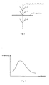
- Fig. 3 shows one example of the line profile obtained in this way.
- the horizontal axis indicates distance, while the vertical axis indicates brightness.
- the obtained line profile is passed into the following line profile feature amount-extracting device 29, where the parameters ⁇ , ⁇ , and ⁇ indicative of the features of the line profile are extracted.
- the aberration calculator 30 enters these parameters, or amounts of features, ⁇ , ⁇ , and ⁇ and computes a parameter C i (where i is an integer) used as a measure indicating each aberration.
- the output from the aberration calculator 30 enters the aberration correction decision-making device 31, which receives the outputs C i 's from the aberration calculator 30 and makes a decision as to whether there still remains aberration to be corrected.
- the feedback amount-setting device 32 finds a field to be applied to the aberration corrector 22 to correct the aberration specified by the aberration correction decision-making device 31 out of the outputs C i 's from the aberration calculator 30.
- Amounts of correction ⁇ Q2x and ⁇ Q3x output from the feedback amount-setting device 32 are entered into the corrector power supply 33.
- This power supply 33 applies voltages for correcting the aberration corrector 22 according to the amounts of correction to the aberration corrector 22.
- the corrector 22 corrects the aberrations in the electron beam. Consequently, the beam free of aberrations can be directed at the specimen S.
- the amount of feedback to be applied to the aberration corrector is automatically calculated in order to correct the aberrations in the electron beam. Consequently, the operator can automatically correct the conditions under which the aberration corrector is driven unconsciously of a complex procedure. Aberrations in the beam can be corrected easily and automatically.
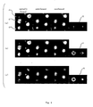
- Fig. 4 illustrates the manner in which artifacts are removed by blurring of the regions close to the four sides, and showphotographs of gray scale images of one example of main image displayed on the viewing screen on a display device in accordance with one embodiment of the invention.
- image regions close to the four sides are not blurred.
- the image regions close to the four sides have been slightly blurred.
- the image regions close to the four sides have been appropriately blurred.
- the left image is obtained when the beam is optimally focused.
- the middle image is obtained when the beam is underfocused.
- the right image is obtained when the beam is overfocused.
- R indicates the profile of each probe.
- the regions close to the four sides can be blurred by adjusting the parameters in this way.
- underfocusing is taken as an example.
- An underfocused image is Fourier-transformed.
- the result is divided by the Fourier transform of the optimally focused image andmultiplied by the inverse Fourier transform of the probe profile when the beam is optimally focused.
- the result is Fourier-transformed.
- the probe profile in an underfocused state is found.
- optimally focused and underfocused images are used.
- the probe profile obtained when the beam is optimally focused is sufficiently smaller than the probe profile when the beam is underfocused. Therefore, it is not necessary to know the profile in detail. Specifically, a Gaussian distribution of a width that is experimentally found using the resolution as a measure will suffice.
- the probe profile is found similarly.
- the method is implemented as follows, for example.
- the root mean square of pixels having sizes less than ⁇ times the maximum value is set to ⁇ .
- the center of gravity of a set of pixels having sizes exceeding ⁇ times the maximum value is given by (i g , j g ).
- the inside of a region whose center is located at (i g , j g ) and which has a radius of r pixels is now considered. Pixels having sizes of more than ⁇ times the ⁇ out of pixels adjacent to the region are added to the region, forming a new region. Pixels having sizes of more than ⁇ times the size E and adjacent to the new region are also added. In this way, pixels are successively added.
- the values of pixels not contained in the finally formed region are set to 0.
- Pixels which are located within the region and have negative values are also set to 0.
- ⁇ and ⁇ are experimentally found parameters.
- ⁇ has a size of about 0.3.
- ⁇ has a size of about 2.
- Probe profiles which have been obtained when the beam is underfocused and overfocused, respectively, and from which noises have been removed in (d) are each represented by a two-dimensional image having m pixels (horizontal) and n pixels (vertical).
- the center of gravity of p u, ij is given by [Mathematical Formula 15]
- the center of gravity of p u, ij is used as the center.
- f u , kl u indicates underfocusing, k indicates direction, and l indicates position.
- line profiles of p o, ij are similarly taken and given by f o , kl .
- the aberration correction decision-making device 31 makes a decision as to whether there still remains aberration to be corrected. For example, the value of Mathematical Formula 18 is found: [Mathematical Formula 18] If the relation C ⁇ ⁇ holds, the adjustment of the aberration correction is ended.
- W i is the weight of each aberration about the decision criterion as to whether convergence has been achieved, and ⁇ is an allowable total amount of aberration.
- the aberration correction decision-making device 31 makes a decision to which aberration should priorly be placed in making a correction.
- Each aberration can be independently quantified.
- C 9 , C 10 , and C 11 have the same symmetry as C 4 , C 5 , and C 6 , respectively, but are higher-order aberrations than the latter aberrations. Therefore, when C 4 , C 5 , and C 6 appear in large amounts, there is the possibility that the accuracy of quantification of C 9 , C 10 , and C 11 deteriorates.
- a threshold value ⁇ i is found about each individual amount of aberration C i . If the threshold value is exceeded, only the corresponding aberration can be corrected.
- a field to be applied to the aberration corrector 22 to correct the aberration specified by the aberration correction decision-making device 31 out of the outputs C 0 to C 11 from the aberration calculator 30 is found.
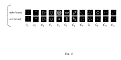
- a case is discussed in which an aberration corrector equipped with four stages of electrodes or magnetic poles produces an x-direction line image in the second stage and a y-direction line image in the third stage.
- Electric quadrupole, hexapole, and octopole fields can be superimposed on each electrode, in addition to the field for creating the first-order orbit as described above.
- These fields are represented, using symbols Q1x to Q4x, Q1y to Q4y, H1x to H4x, H1y to H4y, O1x to O4x, and O1y to O4y, where Q, H, and O represent electric quadrupole, hexapole, and octopole fields, respectively.
- the symbols 1 to 4 indicate what of the four stages of electrodes as counted from the first stage.
- the symbols x and y indicate normal and skewmultipole elements, respectively.
- the normal multipole element referred to herein is a field in which variation of potential around the axis is cos M ⁇ .
- the skew multipole element is a field in which variation of potential around the axis is sinM ⁇ .
- M is an integer indicating the kind of the multipole element, and 2M is the number of the poles.
- ⁇ is the angle around the axis.
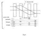
- Fig. 7 shows variations in probe profile when the hexapole field is variedwith the aberration corrector.
- Fig. 7 shows photographs of gray scale images of probe prof iles within picture images displayed on a display device in accordance with one embodiment of the invention.
- the tilt of this straight line is previously foundbya simulation or experiment.
- the aberrations can be corrected by multiplying the outputs C 0 -C 11 from the aberration calculator 30 by the reciprocals of the tilts of straight lines corresponding to the outputs C 0 -C 11 and applying fields that are - 1 times these fields to the aberration corrector 22.
- the feedback gain may be set to about - 0.5 times the reciprocals of the tilts of the straight lines to prevent hunting.
- the feedback gain matrix (described later) becomes a diagonal matrix.
- q2 and q3 should be varied by ⁇ q2 and ⁇ q3, respectively, in order to set both C 4 and C 5 to 0, it being noted that ⁇ q2 and ⁇ q3 are given by [Mathematical Formula 28]
- the feedback gain matrix is a diagonal matrix.
- the aberration-correcting field found in this way is applied to the corrector power supply 33. Since this power supply 33 corrects the aberration corrector 22 according to the input signal, aberrations can be suppressed.
- processing for blurring regions close to the four sides is performed about image data obtained by scanning a specimen with a beam. Consequently, artifacts produced at peripheries of the obtained image can be removed. Hence, the probe profile can be found accurately. Amounts of corrections are computed by the correction amount-calculating means based on the probe profile. Therefore, the amounts of corrections can be calculated precisely.
- automatic method and apparatus can be offered which permit an operator to perform automated correction with ease unconsciously of a complex procedure.
- amounts of features about line profiles are not limited to ⁇ , ⁇ , and ⁇ as in Equations (8)-(10).
- Other amounts indicating the left-and-right asymmetry, width, and unevenness around the center may also be used.
- the conceivable width is not restricted to the standard deviation ⁇ .
- Half-value width and integral 50% width may also be available.
- the feedback amount-setting device may take account of the history of variations in the amounts of aberrations. This also produces the advantage that hunting can be prevented.
- the aforementioned method of correcting aberrations can be applied to every kind of aberration corrector.
- the method can also be applied to the functions of autofocus and autostigmator.
Landscapes
- Chemical & Material Sciences (AREA)
- Analytical Chemistry (AREA)
- Analysing Materials By The Use Of Radiation (AREA)
- Electron Sources, Ion Sources (AREA)
Applications Claiming Priority (2)
| Application Number | Priority Date | Filing Date | Title |
|---|---|---|---|
| JP2003419857 | 2003-12-17 | ||
| JP2003419857A JP2005183085A (ja) | 2003-12-17 | 2003-12-17 | 収差自動補正方法及び装置 |
Publications (2)
| Publication Number | Publication Date |
|---|---|
| EP1544894A2 true EP1544894A2 (de) | 2005-06-22 |
| EP1544894A3 EP1544894A3 (de) | 2011-06-08 |
Family
ID=34510647
Family Applications (1)
| Application Number | Title | Priority Date | Filing Date |
|---|---|---|---|
| EP04257912A Withdrawn EP1544894A3 (de) | 2003-12-17 | 2004-12-17 | Verfahren und Vorrichtung zur Aberrationskorrektur in Ladungsträgerteilchenstrahlen |
Country Status (3)
| Country | Link |
|---|---|
| US (1) | US7145154B2 (de) |
| EP (1) | EP1544894A3 (de) |
| JP (1) | JP2005183085A (de) |
Cited By (3)
| Publication number | Priority date | Publication date | Assignee | Title |
|---|---|---|---|---|
| EP1635373A3 (de) * | 2004-09-14 | 2009-04-29 | Jeol Ltd. | Verfahren zur Korrektur der chromatischen Aberration eines Teilchenstrahls, und Teilchenstrahlapparat |
| WO2023061650A1 (en) * | 2021-10-13 | 2023-04-20 | ICT Integrated Circuit Testing Gesellschaft für Halbleiterprüftechnik mbH | Method of determining the beam convergence of a focused charged particle beam, and charged particle beam system |
| US11810753B2 (en) | 2021-10-13 | 2023-11-07 | ICT Integrated Circuit Testing Gesellschaft für Halbleiterprüftechnik mbH | Methods of determining aberrations of a charged particle beam, and charged particle beam system |
Families Citing this family (8)
| Publication number | Priority date | Publication date | Assignee | Title |
|---|---|---|---|---|
| EP1670028B1 (de) * | 2004-12-07 | 2017-02-08 | JEOL Ltd. | Apparat zur automatischen Korrektur eines Strahls geladener Teilchen |
| JP4881661B2 (ja) * | 2006-06-20 | 2012-02-22 | 株式会社日立ハイテクノロジーズ | 荷電粒子線装置 |
| JP5078431B2 (ja) | 2007-05-17 | 2012-11-21 | 株式会社日立ハイテクノロジーズ | 荷電粒子ビーム装置、その収差補正値算出装置、及びその収差補正プログラム |
| WO2010035386A1 (ja) | 2008-09-25 | 2010-04-01 | 株式会社日立ハイテクノロジーズ | 荷電粒子線応用装置およびその幾何収差測定方法 |
| DE102011009954A1 (de) * | 2011-02-01 | 2012-08-02 | Ceos Corrected Electron Optical Systems Gmbh | Korrektor |
| JP5581248B2 (ja) * | 2011-03-08 | 2014-08-27 | 株式会社日立ハイテクノロジーズ | 走査電子顕微鏡 |
| US9275817B2 (en) * | 2012-04-09 | 2016-03-01 | Frederick Wight Martin | Particle-beam column corrected for both chromatic and spherical aberration |
| US10727024B2 (en) | 2016-08-23 | 2020-07-28 | Hitachi High-Technologies Corporation | Charged particle beam device and aberration correction method for charged particle beam device |
Citations (1)
| Publication number | Priority date | Publication date | Assignee | Title |
|---|---|---|---|---|
| US6282300B1 (en) * | 2000-01-21 | 2001-08-28 | Signafy, Inc. | Rotation, scale, and translation resilient public watermarking for images using a log-polar fourier transform |
Family Cites Families (6)
| Publication number | Priority date | Publication date | Assignee | Title |
|---|---|---|---|---|
| JP3402868B2 (ja) * | 1995-09-14 | 2003-05-06 | 株式会社東芝 | 荷電粒子光学鏡筒における非点収差の補正及び焦点合わせ方法 |
| JP3137084B2 (ja) * | 1998-07-17 | 2001-02-19 | 日本電気株式会社 | 動き検出装置及び方法 |
| DE10003127A1 (de) | 2000-01-26 | 2001-08-02 | Ceos Gmbh | Verfahren zur Ermittlung geometrisch optischer Abbildungsfehler |
| US6723997B2 (en) * | 2001-10-26 | 2004-04-20 | Jeol Ltd. | Aberration corrector for instrument utilizing charged-particle beam |
| JP3914750B2 (ja) * | 2001-11-20 | 2007-05-16 | 日本電子株式会社 | 収差補正装置を備えた荷電粒子線装置 |
| JP2003263634A (ja) * | 2002-03-11 | 2003-09-19 | Noritsu Koki Co Ltd | 画像処理方法、画像処理プログラム、および画像処理プログラムを記録した記録媒体 |
-
2003
- 2003-12-17 JP JP2003419857A patent/JP2005183085A/ja active Pending
-
2004
- 2004-12-17 US US11/016,562 patent/US7145154B2/en not_active Expired - Fee Related
- 2004-12-17 EP EP04257912A patent/EP1544894A3/de not_active Withdrawn
Patent Citations (1)
| Publication number | Priority date | Publication date | Assignee | Title |
|---|---|---|---|---|
| US6282300B1 (en) * | 2000-01-21 | 2001-08-28 | Signafy, Inc. | Rotation, scale, and translation resilient public watermarking for images using a log-polar fourier transform |
Cited By (8)
| Publication number | Priority date | Publication date | Assignee | Title |
|---|---|---|---|---|
| EP1635373A3 (de) * | 2004-09-14 | 2009-04-29 | Jeol Ltd. | Verfahren zur Korrektur der chromatischen Aberration eines Teilchenstrahls, und Teilchenstrahlapparat |
| WO2023061650A1 (en) * | 2021-10-13 | 2023-04-20 | ICT Integrated Circuit Testing Gesellschaft für Halbleiterprüftechnik mbH | Method of determining the beam convergence of a focused charged particle beam, and charged particle beam system |
| US11791128B2 (en) | 2021-10-13 | 2023-10-17 | ICT Integrated Circuit Testing Gesellschaft für Halbleiterprüftechnik mbH | Method of determining the beam convergence of a focused charged particle beam, and charged particle beam system |
| US11810753B2 (en) | 2021-10-13 | 2023-11-07 | ICT Integrated Circuit Testing Gesellschaft für Halbleiterprüftechnik mbH | Methods of determining aberrations of a charged particle beam, and charged particle beam system |
| TWI839863B (zh) * | 2021-10-13 | 2024-04-21 | 德商Ict積體電路測試股份有限公司 | 決定聚焦帶電粒子束的束匯聚度的方法及帶電粒子束系統 |
| CN117981040A (zh) * | 2021-10-13 | 2024-05-03 | Ict半导体集成电路测试有限公司 | 确定聚焦带电粒子束的束汇聚度的方法和带电粒子束系统 |
| KR20240067990A (ko) * | 2021-10-13 | 2024-05-17 | 아이씨티 인티그레이티드 써킷 테스팅 게젤샤프트 퓌어 할프라이터프뤼프테크닉 엠베하 | 집속된 하전 입자 빔의 빔 수렴을 결정하는 방법, 및 하전 입자 빔 시스템 |
| CN117981040B (zh) * | 2021-10-13 | 2024-12-10 | Ict半导体集成电路测试有限公司 | 确定聚焦带电粒子束的束汇聚度的方法和带电粒子束系统 |
Also Published As
| Publication number | Publication date |
|---|---|
| EP1544894A3 (de) | 2011-06-08 |
| US20050156117A1 (en) | 2005-07-21 |
| US7145154B2 (en) | 2006-12-05 |
| JP2005183085A (ja) | 2005-07-07 |
Similar Documents
| Publication | Publication Date | Title |
|---|---|---|
| EP1544893B1 (de) | Verfahren und Vorrichtung zur Aberrationskorrektur in Ladungsträgerteilchenstrahlen | |
| US20090014649A1 (en) | Electron beam apparatus | |
| US7060986B2 (en) | Automated method of correcting aberrations in electron beam, method of visualizing aberrations, and automated aberration corrector | |
| EP1544894A2 (de) | Verfahren und Vorrichtung zur Aberrationskorrektur in Ladungsträgerteilchenstrahlen | |
| JP5603421B2 (ja) | 自動収差補正法を備えた荷電粒子線装置 | |
| US9978561B2 (en) | Post column filter with enhanced energy range | |
| US10014152B2 (en) | Method of aberration correction and charged particle beam system | |
| US20090134339A1 (en) | Electron-optical corrector for aplanatic imaging systems | |
| EP3419043B1 (de) | Verzerrungskorrekturverfahren und elektronenmikroskop | |
| US8785880B2 (en) | Chromatic aberration corrector and electron microscope | |
| US20050035290A1 (en) | Automatic methods for focus and astigmatism corrections in charged-particle beam instrument | |
| Tsuno et al. | Design and testing of Omega mode imaging energy filters at 200 kV | |
| JP4271037B2 (ja) | 粒子光学補正器 | |
| US7355175B2 (en) | Method and apparatus for automatically correcting charged-particle beam and method of controlling aberration corrector for charged-particle beam | |
| EP2600382A1 (de) | Aberrationskorrekturvorrichtung und ladungsträgerstrahlvorrichtung damit | |
| JP3340327B2 (ja) | 非点収差補正方法及び非点収差補正装置 | |
| JP4522203B2 (ja) | 荷電粒子ビーム装置の色収差補正方法及び装置並びに荷電粒子ビーム装置 | |
| WO2021100172A1 (ja) | 荷電粒子線装置及び収差補正方法 | |
| JP2000149850A (ja) | 荷電粒子線装置 | |
| JP3369894B2 (ja) | 非点収差補正方法及び非点収差補正装置 | |
| EP3731255B1 (de) | Energiefilter und vorrichtung für geladene teilchenstrahlen | |
| JP4328257B2 (ja) | 荷電粒子ビーム装置の収差自動補正方法及び装置 | |
| KR20250146287A (ko) | 구성 변화에 의한 입자빔 시스템들에서의 에너지 의존 디포커스의 자동 보정 |
Legal Events
| Date | Code | Title | Description |
|---|---|---|---|
| PUAI | Public reference made under article 153(3) epc to a published international application that has entered the european phase |
Free format text: ORIGINAL CODE: 0009012 |
|
| AK | Designated contracting states |
Kind code of ref document: A2 Designated state(s): AT BE BG CH CY CZ DE DK EE ES FI FR GB GR HU IE IS IT LI LT LU MC NL PL PT RO SE SI SK TR |
|
| AX | Request for extension of the european patent |
Extension state: AL BA HR LV MK YU |
|
| PUAL | Search report despatched |
Free format text: ORIGINAL CODE: 0009013 |
|
| AK | Designated contracting states |
Kind code of ref document: A3 Designated state(s): AT BE BG CH CY CZ DE DK EE ES FI FR GB GR HU IE IS IT LI LT LU MC NL PL PT RO SE SI SK TR |
|
| AX | Request for extension of the european patent |
Extension state: AL BA HR LV MK YU |
|
| 17P | Request for examination filed |
Effective date: 20111207 |
|
| AKX | Designation fees paid |
Designated state(s): DE FR GB |
|
| 17Q | First examination report despatched |
Effective date: 20160120 |
|
| STAA | Information on the status of an ep patent application or granted ep patent |
Free format text: STATUS: THE APPLICATION IS DEEMED TO BE WITHDRAWN |
|
| 18D | Application deemed to be withdrawn |
Effective date: 20160802 |