EP1544893B1 - Verfahren und Vorrichtung zur Aberrationskorrektur in Ladungsträgerteilchenstrahlen - Google Patents
Verfahren und Vorrichtung zur Aberrationskorrektur in Ladungsträgerteilchenstrahlen Download PDFInfo
- Publication number
- EP1544893B1 EP1544893B1 EP04257911.0A EP04257911A EP1544893B1 EP 1544893 B1 EP1544893 B1 EP 1544893B1 EP 04257911 A EP04257911 A EP 04257911A EP 1544893 B1 EP1544893 B1 EP 1544893B1
- Authority
- EP
- European Patent Office
- Prior art keywords
- aberrations
- aberration
- image
- amount
- charged
- Prior art date
- Legal status (The legal status is an assumption and is not a legal conclusion. Google has not performed a legal analysis and makes no representation as to the accuracy of the status listed.)
- Ceased
Links
- 230000004075 alteration Effects 0.000 title claims description 168
- 239000002245 particle Substances 0.000 title claims description 30
- 238000000034 method Methods 0.000 title claims description 25
- 239000000523 sample Substances 0.000 claims description 49
- 230000005405 multipole Effects 0.000 claims description 35
- 239000011159 matrix material Substances 0.000 claims description 18
- 238000012937 correction Methods 0.000 description 33
- 238000010894 electron beam technology Methods 0.000 description 7
- 238000010586 diagram Methods 0.000 description 5
- 230000005684 electric field Effects 0.000 description 5
- 238000013461 design Methods 0.000 description 4
- 230000005284 excitation Effects 0.000 description 4
- 239000000284 extract Substances 0.000 description 4
- 230000005484 gravity Effects 0.000 description 4
- 230000003287 optical effect Effects 0.000 description 3
- 238000011002 quantification Methods 0.000 description 3
- 206010010071 Coma Diseases 0.000 description 2
- 230000009471 action Effects 0.000 description 2
- 230000003213 activating effect Effects 0.000 description 2
- 201000009310 astigmatism Diseases 0.000 description 2
- 230000008901 benefit Effects 0.000 description 2
- 238000012545 processing Methods 0.000 description 2
- 101100042630 Caenorhabditis elegans sin-3 gene Proteins 0.000 description 1
- 230000004913 activation Effects 0.000 description 1
- 230000005540 biological transmission Effects 0.000 description 1
- 238000004364 calculation method Methods 0.000 description 1
- 230000000694 effects Effects 0.000 description 1
- 238000002474 experimental method Methods 0.000 description 1
- 230000006870 function Effects 0.000 description 1
- 238000003384 imaging method Methods 0.000 description 1
- 239000000696 magnetic material Substances 0.000 description 1
- MYWUZJCMWCOHBA-VIFPVBQESA-N methamphetamine Chemical compound CN[C@@H](C)CC1=CC=CC=C1 MYWUZJCMWCOHBA-VIFPVBQESA-N 0.000 description 1
- 238000004088 simulation Methods 0.000 description 1
Images


Classifications
-
- H—ELECTRICITY
- H01—ELECTRIC ELEMENTS
- H01J—ELECTRIC DISCHARGE TUBES OR DISCHARGE LAMPS
- H01J37/00—Discharge tubes with provision for introducing objects or material to be exposed to the discharge, e.g. for the purpose of examination or processing thereof
- H01J37/26—Electron or ion microscopes; Electron or ion diffraction tubes
- H01J37/28—Electron or ion microscopes; Electron or ion diffraction tubes with scanning beams
-
- H—ELECTRICITY
- H01—ELECTRIC ELEMENTS
- H01J—ELECTRIC DISCHARGE TUBES OR DISCHARGE LAMPS
- H01J37/00—Discharge tubes with provision for introducing objects or material to be exposed to the discharge, e.g. for the purpose of examination or processing thereof
- H01J37/02—Details
- H01J37/04—Arrangements of electrodes and associated parts for generating or controlling the discharge, e.g. electron-optical arrangement or ion-optical arrangement
- H01J37/153—Electron-optical or ion-optical arrangements for the correction of image defects, e.g. stigmators
Definitions
- the present invention relates to a method of automatically correcting aberrations in a charged-particle beam and to an apparatus therefor.
- an aberration corrector is built in the electron optical system to permit high-resolution imaging and to enhance the probe current density.
- a system consisting of an aberration corrector having four stages of multipole units is proposed as the first-mentioned built-in aberration corrector.
- Each multipole unit has 12 pole elements.
- Chromatic aberration is corrected by a combination of an electrostatic quadrupole mode of operation and a magnetic quadrupole mode of operation.
- Spherical aberration is corrected by four stages of octopole mode of operation. The principle is introduced in detail in Non-Patent References 1 to 3.
- an aberration corrector C is disposed ahead of an objective lens 7 and equipped with four stages of multipole units 51, 52, 53, and 54.
- Each of the multipole units 51-54 has 12 pole elements.
- Electric potentials 1, 2, 3, and 4 are applied to the multipole elements 51-54, respectively, to activate the electrostatic quadrupole elements.
- Exciting currents 5 and 6 are supplied to the second and third stages of multipole units 52 and 53, respectively, toproducemagnetic potential distribution analogous to the electric potential distribution created by the potentials 2 and 3 and to produce a magnetic field superimposed on the electric field.
- electric potentials 11, 12, 13, and 14 are applied to the multipole units 51-54, respectively, to activate an electrostatic octopole element for producing an electric field superimposed on the electric field produced by the potentials 1-4 that are used to activate the quadrupole.
- a reference orbit for the beam B is created by the four stages of multipole units 51-54 and objective lens 7.
- the beam B is focused onto a specimen surface 20.
- X-direction orbit R x and Y-direction orbit R y of the beam B are both schematically drawn on the same plane.
- the reference orbit can be understood as a paraxial orbit that is assumed when there is no aberration. That is, the Y-direction orbit R y is made to pass through the center of the multipole unit 52 by the multipole unit 51. The X-direction orbit R x is made to pass through the center of the multipole unit 53 by the multipole unit 52. Finally, the charged-particle beam B is focused onto the specimen surface 20 by the multipole units 53, 54 and objective lens 7. In practice, these need to be adjusted mutually for complete focusing. At this time, the dipole-activating potentials applied to the four stages of multipole units 51-54 are used for axial alignment.
- the charged-particle beam B in the X-direction orbit R x is diffused by the multipole unit 51 acting like a concave lens. Then, the beam is focused by the multipole unit 52 acting like a convex lens and made to pass through the center of the multipole unit 53. Then, the beam is focused by the multipole unit 54 and moves toward the objective lens 7.
- the beam B in the Y-direction orbit R y is focused by the multipole unit 51 and made to pass through the center of the multipole unit 52. Then, the beam is focused by the multipole unit 53. Finally, the beam is diffused by the multipole unit 54 and moves toward the objective lens 7.
- the electron optical system can be operated like a single concave or convex lens.
- Spherical aberration is corrected after X- and Y-direction chromatic aberrations are corrected.
- the X-direction spherical aberration in the whole lens system is corrected to zero by electric potential ⁇ 02 [V] acting as an electrostatic octopole element.
- the Y-direction spherical aberration is corrected to zero by electric potential ⁇ 03 [V] acting as an electrostatic octopole element.
- output voltages from a quadrupole power supply 10 are supplied to the final-stage power supplies An to obtain a field close to an ideal quadrupole field. If it is assumed that the output voltages from the final-stage power supplies A n are proportional to the output voltages from the quadrupole power supply 10, the ratio of the output voltages from the power supply 10 assumes a value as given in the above-quoted Non-Patent Reference 4.
- output voltages from an octopole power supply 18 are added to the output voltages from the quadrupole power supply 10 and supplied to the final-stage power supplies A n to obtain a field close to an ideal octopole field.
- output voltages from a magnetic quadrupole power supply 15 are supplied to the final stage of power supplies B n to produce a field close to an ideal magnetic quadrupole field. If it is assumed that the output currents from the final-stage power supplies B n are proportional to the output voltage from the magnetic quadrupole power supply 15, the ratio of the output voltages assumes an exciting magnetic force ratio as given in the above-quotedNon-Patent Reference 4.
- a magnetic multipole field can be superimposed in the same way as in the electrostatic design, by adding voltages for multipole fields to the input voltage to the final-stage power supplies B n .
- a yoke for magnetically connecting the outside portions of the magnets W n is omitted in Fig. 10 .
- a conductive magnetic material may be used so that the magnets W n can act also as the electrodes U n .
- the coils on the magnets are disposed so as to be electrically isolated from the electrodes.
- the second-order aperture aberration After end of correction of chromatic aberration in the charged-particle beam B, it may be necessary to correct the second-order aperture aberration by means of three or four stages of hexapole elements before the correction of spherical aberration is performed. This correction is made in the same procedure as in the aforementioned correction of spherical aberration.
- This second-order aperture aberration occurs depending on the mechanical accuracy of the aberration corrector. Normally, the amount of correction is small, and this aberration affects higher-order aberrations only a little within the scope of the present aberration corrector. Furthermore, the second-order aperture aberration is corrected within the aberration corrector.
- a method of detecting geometric optics aberrations up to the third order using a probe is known, for example, as described in Patent Reference 1.
- Patent Reference 1 Unexamined Japan Patent Number P2003-521801 (paragraphs 0006-0008, Fig. 1 )
- US2003/0001102A1 discloses a method for detecting geometric-optical aberrations for a scanning electron microscope according to the preamble of claims 1 and 2.
- the present invention has been made. It would be desirable to provide a method and apparatus permitting an operator to automatically and easily correct aberrations in a charged-particle beam unconsciously of a complex procedure of aberration correction.
- a method of automatically correcting aberrations in a charged-particle beam in accordance with the present invention is defined by claim 1.
- An apparatus for automatically correcting aberrations in a charged-particle beam in accordance with the present invention is defined by claim 2.
- a preferred embodiment of the present invention is defined in claim 3.
- the amount of feedback to be applied to the aberration corrector to correct the aberrations in the beam is automatically calculated. Therefore, the operator can easily and automatically correct the aberrations in the beam unconsciously of a complex procedure.
- the amount of feedback to be applied to the aberration corrector to correct the aberrations in the beam is automatically calculated using various processing circuits. Consequently, the operator can easily and automatically correct the aberrations in the beam unconsciously of a complex procedure.
- Fig. 1 shows the configuration of one embodiment of the present invention.
- indicated by numeral 21 is the body of an apparatus having the configuration of an SEM.
- An aberration corrector 22 is mounted in the body 21 of the apparatus.
- the corrector 22 is designed as shown in Fig. 8 .
- the body 21 of the apparatus has a specimen chamber 21a in which a specimen S is placed.
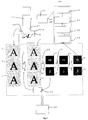
- a character "A" as shown is formed on the surface of the specimen S.
- the specimen S is irradiated with an electron beam that is one kind of charged-particle beam.
- secondary electrons and other electrons are emitted from the surface of the specimen S .
- the secondary electrons are detected by a detector 23.
- a to C show specimen images detected by the detector 23.
- the image A is obtained when the beam is accurately focused.
- the image B is obtained when the beam is underfocused.
- the image C is obtained when the beam is overfocused.
- Fig. 2 shows the state in which the electron beam is focused onto a specimen.
- the specimen is indicated by numeral 15.
- the optical axis of the beam is indicated by numeral 16.
- a indicates the state in which the beam is focused above the specimen
- b indicates the state in which the beam is focused onto a surface of the specimen
- c indicates the state in which the beam is focused under the surface of the specimen 15.
- the beam is excessively restricted by a lens and so the beam is focused above the surface of the specimen 15.
- the beam is accurately focused onto the surface of the specimen 15.
- the state c the beam is insufficiently restricted, so that the beam is focused under the surface of the specimen 15.
- the image b the image is blurred laterally.
- the image C the image is blurred vertically.
- the image detected by the detector 23 is converted into a digital image and then stored in a memory 35.
- a four-side region-blurring device 24 reads each image stored in the memory 35 and blurs regions close to the four sides of the image.
- the probe profile extractor 25 receives the output from the blurring device 24 and extracts the profile of each probe.
- A', B', and C' are images respectively obtained after the images A, B, and C have passed through the blurring device 24.
- An S/N adjuster 26 adjusts the S/N of the image extracted by the probe profile extractor 25 and reduces the noise. The output from the S/N adjuster 26 is fed back to the four-side region-blurring device 24, where the background noise is removed.
- D indicates the cross-sectional shape of the electron probe when the beam is underfocused
- E indicates the cross-sectional shape of the probe when the beam is overfocused.
- the cross-sectional shape of the electron probe may hereinafter be referred to as the profile of the probe.
- a noise remover 27 receives the output from the probe profile extractor 25 and removes the noise.
- a line profile extractor 28 sets lines as shown for the probe profile from which the noise has been removed, and extracts line profiles in the directions of the lines.
- F indicates the state in which the lines are set for an underfocused probe.
- G indicates the state in which the lines are set for an overfocused probe.
- Each line profile is entered into the correction amount-calculating means 40, where the "amount of correction to aberration" is computed.
- a corrector power supply 33 adds the "amount of correction to aberration” to the aberration corrector 22 based on the amount of correction computed by the calculating means 40.
- a line profile feature amount-extracting device 29 receives the output from the line profile extractor 28 and extracts amounts of features of the line profile.
- the amounts of features consist of ⁇ indicating the left-and-right asymmetry of the line profile, ⁇ indicating the width of the line profile, and ⁇ indicating the unevenness around the center of the line profile.
- An aberration calculator 30 receives the output from the line profile feature amount-extracting device 29 and calculates parameters C i 's indicating aberrations (where i is an integer).
- An aberration correction decision-making device 31 receives the output from the aberration calculator 30 and makes a decision as to whether there still remains aberration to be corrected.
- a feedback amount-setting device 32 receives the output from the decision-making device 31 and sets an amount of feedback to reduce the aberration.
- the corrector power supply 33 receives the output from the setting device 32 and produces an output that drives the aberration corrector 22.
- a memory 35 stores specimen images taken in. For example, a magnetic disk drive is used as this memory 35. The operation of the apparatus constructed in this way is described below.
- the electron beam emitted from an electron gun passes through the aberration corrector 22. At this time, the beam undergoes an aberration correction and is focused on the specimen S. Secondary electrons or backscattered electrons produced from the surface of the specimen are detected by the detector 23. Then, the output signal from the detector 23 is converted into digital image data by an A/D converter (not shown) and then stored in the memory 35.
- Each image stored in the memory 35 can take one of three states; one ( b ) is precisely focused state of the electron beam as shown in Fig. 2 , another ( c ) is an underfocused state, and the remaining one ( a ) is an overfocused state.
- the image data stored in the memory 35 is read out and then enters the four-side region-blurring device 24, where artifacts around the four sides of the image are removed.
- the images blurred in this way by the four-side region-blurring device 24 are indicated by A', B', and C', respectively.
- the probe profile extractor 25 extracts the probe profile. Examples of probes whose profiles have been extracted by the extracting device 25 are indicated by D and E.
- D indicates the profile obtained in an underfocused state.
- E indicates the profile obtained in an overfocused state.
- the image of the profile of each probe is automatically adjusted by the S/N adjuster 26 and fed back to the four-side region-blurring device 24. In consequence, the average size of background noises contained in the probe profile can be reduced to a minimum.
- Fig. 3 shows one example of the line profile obtained in this way.
- the horizontal axis indicates distance, while the vertical axis indicates brightness.
- the obtained line profile is passed into the following line profile feature amount-extracting device 29, where the parameters ⁇ , ⁇ , and ⁇ indicative of the features of the line profile are extracted.
- the aberration calculator 30 enters these parameters, or amounts of features ⁇ , ⁇ , and ⁇ , and computes a parameter C i (where i is an integer) used as a measure indicating each aberration.
- the output from the aberration calculator 30 enters the aberration correction decision-making device 31, which receives the outputs C i ' s from the aberration calculator 30 and makes a decision as to whether there still remains aberration to be corrected.
- the feedback amount-setting device 32 finds a field to be applied to the aberration corrector 22 to correct the aberration specified by the aberration correction decision-making device 31 out of the outputs C i 's from the aberration calculator 30.
- Amounts of correction ⁇ Q2x and ⁇ Q3x output from the feedback amount-setting device 32 are entered into the corrector power supply 33.
- This power supply 33 applies voltages for correcting the aberration corrector 22 according to the amounts of correction to the aberration corrector 22.
- the corrector 22 corrects the aberrations in the electron beam. Consequently, the beam free of aberrations can be directed at the specimen S.
- the amount of feedback to be applied to the aberration corrector is automatically calculated in order to correct the aberrations in the electron beam. Consequently, the operator can automatically correct the conditions under which the aberration corrector is driven unconsciously of a complex procedure. Aberrations in the beam can be corrected easily and automatically.
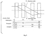
- Electric quadrupole, hexapole, and octopole fields can be superimposed on each electrode, in addition to the field for creating the first-order orbit as described above .
- These fields are represented, using symbols Q1x to Q4x, Q1y to Q4y, H1x to H4x, H1y to H4y, O1x to O4x, and O1y to O4y, where Q, H, and O represent electric quadrupole, hexapole, and octopole fields, respectively.
- the symbols 1 to 4 indicate what of the four stages of electrodes as counted from the first stage.
- the symbols x and y indicate normal and skewmultipole elements, respectively.
- the normal multipole element referred to herein is a field in which variation of potential around the axis is cos M ⁇ .
- the skew multipole element is a field in which variation of potential around the axis is sin M ⁇ .
- M is an integer indicating the kind of the multipole element, and 2M is the number of the poles.
- ⁇ is the angle around the axis.
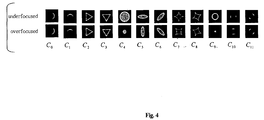
- Fig. 6 shows variations in probe profile when the hexapole field is varied with the aberration corrector.
- Fig. 6 shows photographs of gray scale images of probe profiles within picture images displayed on a display device in accordance with one embodiment of the invention.
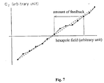
- the tilt of this straight line ispreviously found by a simulation or experiment.
- the aberrations can be corrected by multiplying the outputs C 0 -C 11 from the aberration calculator 30 by the reciprocals of the tilts of straight lines corresponding to the outputs C 0 -C 11 and applying fields that are - 1 times these fields to the aberration corrector 22.
- the feedback gain may be set to about - 0.5 times the reciprocals of the tilts of the straight lines to prevent hunting.
- the feedback gain matrix (described later) becomes a diagonal matrix.
- a C B D is the inverse matrix of a c b d
- C 4 and C 5 can both be set to 0 by varying Q2x and Q3x by ⁇ Q2x and ⁇ Q3x, respectively, which are given by
- ⁇ q2 and ⁇ q3 can be found as linear combinations of C 4 and C 5 .
- the feedback gain matrix is a diagonal matrix.
- Equation (32) Where the fields of Q2x and Q3x are used as in Equation (32), four values A, B, C, and D must be adjusted when the feedback gain is experimentally adjusted or automatically varied.
- the fields of q2 and q3 are used as in Equation (35), the feedback gain matrix is a diagonal matrix. Therefore, there are two parameters to be adjusted. Also, there is a direct relationship between the aberration and field. These facilitate understanding.
- the aberration-correcting field found in this way is applied to the corrector power supply 33. Since this power supply 33 corrects the aberration corrector 22 according to the input signal, aberrations can be suppressed.
- the amount of feedback to be applied to the aberration corrector to correct the aberrations in the charged-particle beam is automatically calculated using various processing circuits. Therefore, the operator can automatically correct the aberrations in the beam easily and unconsciously of a complex procedure.
- the four-side region-blurring device may be omitted.
- amounts of features about line profiles are not limited to ⁇ , ⁇ , and ⁇ as in Equations (3)-(5).
- Other amounts indicating the left-and-right asymmetry, width, and unevenness around the center may also be used.
- the conceivable width is not restricted to the standard deviation ⁇ .
- Half-value width and integral 50% width may also be available.
- the feedback amount-setting device may take account of the history of variations in the amounts of aberrations. This also produces the advantage that hunting can be prevented.
- the aforementioned method of correcting aberrations can be applied to every kind of aberration corrector.
- the method can also be applied to the functions of autofocus and autostigmator.
Landscapes
- Chemical & Material Sciences (AREA)
- Analytical Chemistry (AREA)
- Length-Measuring Devices Using Wave Or Particle Radiation (AREA)
- Analysing Materials By The Use Of Radiation (AREA)
- Electron Beam Exposure (AREA)
- Electron Sources, Ion Sources (AREA)
Claims (3)
- Verfahren zur automatischen Korrektur von Aberrationen in einem Strahl geladener Teilchen, wobei das Verfahren die folgenden Schritte umfasst:Bereitstellung eines optimal fokussierten Bildes (A), eines unterfokussierten Bildes (B) und eines überfokussierten Bildes (C) einer Sonde;Extraktion eines Sondenprofils (D) des unterfokussierten Bildes aus der Fourier-Transformierten des unterfokussierten Bildes und der Fourier-Transformierten des optimal fokussierten Bildes;Extraktion eines Sondenprofils (E) des überfokussierten Bildes aus der Fourier-Transformierten des überfokussierten Bildes und der Fourier-Transformierten des optimal fokussierten Bildes;Extraktion von Linienprofilen (F, G) aus den Sondenprofilen (D, E) des Strahls geladener Teilchen, wenn dieser unterfokussiert und überfokussiert worden ist;Berechnung von Mengen von Funktionen oder Merkmalen µ, σ, und ρ (µu,k, σu,k, ρu,k, µo,k, σo,k ρo,k) aus den extrahierten Linienprofilen, wenn der Strahl geladener Teilchen unterfokussiert oder überfokussiert worden ist, wobei µ, σ, und ρ Funktionen oder Merkmale der Linienprofile anzeigen, d.h. Rechts-Links-Asymmetrie, Breite und Ungleichmäßigkeiten um die Mitte;Berechnung von Mengen von Aberrationen (C0 bis C11) in dem Strahl geladener Teilchen aus den Mengen von Funktionen oder Merkmalen µ, σ, und ρ (µu,k, σu,k, ρu,k, µo,k, σo,k ρo,k);wobei das Verfahren weiter dadurch gekennzeichnet ist, dass es die folgenden Schritte umfasst:Treffen einer Entscheidung, ob die Gesamtmenge von Aberrationen in dem Strahl geladener Teilchen, welche basierend auf den Mengen von Aberrationen berechnet wird, kleiner ist als ein vorgegebener Schwellenwert;Spezifizieren zumindest einer Menge der Mengen von Aberrationen, Berechnen einer Feedback-Menge zur Verringerung der spezifizierten Menge von Aberrationen, sowie Korrigieren der Aberrationen in dem Strahl geladener Teilchen basierend auf der Feedback-Menge, wenn von dem Schritt des Treffens einer Entscheidung beurteilt worden ist, dass die Gesamtmenge von Aberrationen größer ist als der Schwellenwert ; undBerechnen der Feedback-Menge unter Verwendung von Feldern, welche aus einer Feedback-Verstärkungsmatrix eine diagonale Matrix machen, wobei die Feedback-Verstärkungsmatrix Beziehungen zwischen der Feedback-Menge und den Mengen von Aberrationen anzeigt.
- Vorrichtung zur automatischen Korrektur von Aberrationen in einem Strahl geladener Teilchen, wobei die Vorrichtung Folgendes umfasst:eine Einrichtung (23) zur Bereitstellung eines optimal fokussierten Bildes (A), eines unterfokussierten Bildes (B) und eines überfokussierten Bildes (C) einer Sonde;einen Sondenprofil-Extraktor (25) zur Extraktion eines Sondenprofils (D) des unterfokussierten Bildes aus der Fourier-Transformierten des unterfokussierten Bildes und der Fourier-Transformierten des optimal fokussierten Bildes, und zur Extraktion des Sondenprofils (E) des überfokussierten Bildes aus der Fourier-Transformierten des überfokussierten Bildes und der Fourier-Transformierten des optimal fokussierten Bildes;einen Linienprofil-Extraktor (28) zur Extraktion von Linienprofilen (F, G) aus den Sondenprofilen (D, E) des Strahls geladener Teilchen, wenn dieser unterfokussiert und überfokussiert worden ist;einen Linienprofil-Funktionsmengen-Extraktor (29) zur Berechnung von Mengen von Funktionen oder Merkmalen µ, σ, und ρ (µu,k, σu,k, ρu,k, µo,k, σo,k ρo,k) aus den extrahierten Linienprofilen, wenn der Strahl geladener Teilchen unterfokussiert oder überfokussiert worden ist, wobei µ, σ, und ρ Funktionen oder Merkmale der Linienprofile anzeigen, d.h. Rechts-Links-Asymmetrie, Breite und Ungleichmäßigkeiten um die Mitte;einen Aberrationsmengen-Kalkulator (30) zur Berechnung von Aberrationsmengen (C0 bis C11) in dem Strahl geladener Teilchen aus den Mengen von Funktionen oder Merkmalen µ, σ, und ρ (µu,k, σu,k, ρu,k, µo,k, σok ρo,k);wobei die Vorrichtung dadurch gekennzeichnet ist, dass sie des Weiteren Folgendes umfasst:eine Aberrationsmengen-Entscheidungsvorrichtung (31) zum Treffen einer Entscheidung, ob eine Gesamtmenge von Aberrationen in dem Strahl geladener Teilchen, welche basierend auf den Aberrationsmengen berechnet worden ist, kleiner ist als ein vorgegebener Schwellenwert;eine Feedbackmengen-Einstellvorrichtung (32) zum Spezifizieren zumindest einer Menge der Mengen von Aberrationen, Berechnen einer Feedback-Menge zur Verringerung der spezifizierten Menge von Aberrationen;einen Aberrations-Korrektor (22) zur Korrektur der Aberrationen in dem Strahl geladener Teilchen basierend auf der Feedback-Menge,wobei die Feedbackmengen-Einstellvorrichtung (32) die Feedback-Menge als eine lineare Kombination der Mengen von Aberrationen vorfindet, welche durch Ausgangssignale aus dem Aberrations-Rechner (30) angezeigt werden und die Feedback-Menge berechnet, indem sie Felder verwendet, welche aus einer Feedback-Verstärkungsmatrix eine diagonale Matrix machen, wobei die Feedback-Verstärkungsmatrix Beziehungen zwischen der Feedback-Menge und den Mengen von Aberrationen anzeigt.
- Vorrichtung zur automatischen Korrektur von Aberrationen in einem Strahl geladener Teilchen nach Anspruch 2, wobei der Aberrations-Korrektor (22) aus vier Abschnitten von Multipol-Elementen zusammengesetzt ist, und wobei Zeilenbilder des Strahls geladener Teilchen in zweiten und dritten Abschnitten des Korrektors erzeugt werden.
Applications Claiming Priority (2)
| Application Number | Priority Date | Filing Date | Title |
|---|---|---|---|
| JP2003419858A JP4248387B2 (ja) | 2003-12-17 | 2003-12-17 | 収差自動補正方法及び装置 |
| JP2003419858 | 2003-12-17 |
Publications (3)
| Publication Number | Publication Date |
|---|---|
| EP1544893A2 EP1544893A2 (de) | 2005-06-22 |
| EP1544893A3 EP1544893A3 (de) | 2011-06-08 |
| EP1544893B1 true EP1544893B1 (de) | 2016-08-10 |
Family
ID=34510648
Family Applications (1)
| Application Number | Title | Priority Date | Filing Date |
|---|---|---|---|
| EP04257911.0A Ceased EP1544893B1 (de) | 2003-12-17 | 2004-12-17 | Verfahren und Vorrichtung zur Aberrationskorrektur in Ladungsträgerteilchenstrahlen |
Country Status (3)
| Country | Link |
|---|---|
| US (1) | US7095031B2 (de) |
| EP (1) | EP1544893B1 (de) |
| JP (1) | JP4248387B2 (de) |
Families Citing this family (13)
| Publication number | Priority date | Publication date | Assignee | Title |
|---|---|---|---|---|
| JP4522203B2 (ja) * | 2004-09-14 | 2010-08-11 | 日本電子株式会社 | 荷電粒子ビーム装置の色収差補正方法及び装置並びに荷電粒子ビーム装置 |
| JP4988216B2 (ja) * | 2006-02-03 | 2012-08-01 | 株式会社日立ハイテクノロジーズ | 収差補正装置を搭載した荷電粒子線装置 |
| JP4857101B2 (ja) * | 2006-12-21 | 2012-01-18 | 株式会社日立ハイテクノロジーズ | プローブ評価方法 |
| JP5078431B2 (ja) * | 2007-05-17 | 2012-11-21 | 株式会社日立ハイテクノロジーズ | 荷電粒子ビーム装置、その収差補正値算出装置、及びその収差補正プログラム |
| DE102007049816B3 (de) * | 2007-10-20 | 2009-04-16 | Ceos Corrected Electron Optical Systems Gmbh | Korrektor |
| JP5028297B2 (ja) * | 2008-02-22 | 2012-09-19 | 株式会社日立ハイテクノロジーズ | 収差補正器を備えた荷電粒子線装置 |
| JP5188846B2 (ja) * | 2008-03-10 | 2013-04-24 | 日本電子株式会社 | 走査型透過電子顕微鏡の収差補正装置及び収差補正方法 |
| DE102011009954A1 (de) * | 2011-02-01 | 2012-08-02 | Ceos Corrected Electron Optical Systems Gmbh | Korrektor |
| JP5581248B2 (ja) * | 2011-03-08 | 2014-08-27 | 株式会社日立ハイテクノロジーズ | 走査電子顕微鏡 |
| JP5777984B2 (ja) | 2011-09-08 | 2015-09-16 | 株式会社日立ハイテクノロジーズ | 多極子測定装置 |
| JP5806942B2 (ja) * | 2012-01-19 | 2015-11-10 | 株式会社日立ハイテクノロジーズ | 荷電粒子線装置及び演算装置 |
| US9275817B2 (en) * | 2012-04-09 | 2016-03-01 | Frederick Wight Martin | Particle-beam column corrected for both chromatic and spherical aberration |
| US10727024B2 (en) | 2016-08-23 | 2020-07-28 | Hitachi High-Technologies Corporation | Charged particle beam device and aberration correction method for charged particle beam device |
Family Cites Families (8)
| Publication number | Priority date | Publication date | Assignee | Title |
|---|---|---|---|---|
| JPH06105598B2 (ja) * | 1992-02-18 | 1994-12-21 | 工業技術院長 | 荷電ビーム用レンズ |
| US6025600A (en) * | 1998-05-29 | 2000-02-15 | International Business Machines Corporation | Method for astigmatism correction in charged particle beam systems |
| DE10003127A1 (de) | 2000-01-26 | 2001-08-02 | Ceos Gmbh | Verfahren zur Ermittlung geometrisch optischer Abbildungsfehler |
| US6723997B2 (en) * | 2001-10-26 | 2004-04-20 | Jeol Ltd. | Aberration corrector for instrument utilizing charged-particle beam |
| JP3914750B2 (ja) * | 2001-11-20 | 2007-05-16 | 日本電子株式会社 | 収差補正装置を備えた荷電粒子線装置 |
| DE10159454B4 (de) * | 2001-12-04 | 2012-08-02 | Carl Zeiss Nts Gmbh | Korrektor zur Korrektion von Farbfehlern erster Ordnung, ersten Grades |
| JP3979945B2 (ja) * | 2003-01-23 | 2007-09-19 | 日本電子株式会社 | 電子分光系を有した電子線装置 |
| JP4133602B2 (ja) * | 2003-06-06 | 2008-08-13 | 日本電子株式会社 | 荷電粒子ビーム装置における収差補正方法および荷電粒子ビーム装置 |
-
2003
- 2003-12-17 JP JP2003419858A patent/JP4248387B2/ja not_active Expired - Fee Related
-
2004
- 2004-12-17 EP EP04257911.0A patent/EP1544893B1/de not_active Ceased
- 2004-12-17 US US11/016,687 patent/US7095031B2/en not_active Expired - Fee Related
Also Published As
| Publication number | Publication date |
|---|---|
| US20050189496A1 (en) | 2005-09-01 |
| JP2005183086A (ja) | 2005-07-07 |
| EP1544893A3 (de) | 2011-06-08 |
| EP1544893A2 (de) | 2005-06-22 |
| JP4248387B2 (ja) | 2009-04-02 |
| US7095031B2 (en) | 2006-08-22 |
Similar Documents
| Publication | Publication Date | Title |
|---|---|---|
| EP1544893B1 (de) | Verfahren und Vorrichtung zur Aberrationskorrektur in Ladungsträgerteilchenstrahlen | |
| US6924488B2 (en) | Charged-particle beam apparatus equipped with aberration corrector | |
| US20090014649A1 (en) | Electron beam apparatus | |
| US8178850B2 (en) | Chromatic aberration corrector for charged-particle beam system and correction method therefor | |
| US7714286B2 (en) | Charged particle beam apparatus, aberration correction value calculation unit therefor, and aberration correction program therefor | |
| US7060986B2 (en) | Automated method of correcting aberrations in electron beam, method of visualizing aberrations, and automated aberration corrector | |
| EP2325862A1 (de) | Korrektor für axiale Aberrationen einer teilchenoptischen Linse | |
| US9349565B2 (en) | Multipole lens, aberration corrector, and electron microscope | |
| US20030098415A1 (en) | Aberration corrector for instrument utilizing charged-particle beam | |
| KR19990028770A (ko) | 입자-광학 장치에서 렌즈 수차를 교정하기 위한 교정장치 | |
| EP2166557A1 (de) | Verfahren zur Berichtigung von Verzerrungen in einer teilchenoptischen Vorrichtung | |
| US10431420B2 (en) | Post column filter with enhanced energy range | |
| US7145154B2 (en) | Method of automatically correcting aberrations in charged-particle beam and apparatus therefor | |
| EP1441382B1 (de) | Elektronenstrahl-Vorrichtung mit Elektronenenergie-Analysator, Einrichtung und Methode zur Steuerung von Linsen | |
| US20140158901A1 (en) | Chromatic aberration corrector and electron microscope | |
| JP2019008880A (ja) | 歪み補正方法および電子顕微鏡 | |
| EP0883891A2 (de) | Verfahren zum betreiben eines partikels optischen gerätes | |
| US20040155200A1 (en) | Optical particle corrector | |
| US7060985B2 (en) | Multipole field-producing apparatus in charged-particle optical system and aberration corrector | |
| EP1635373B1 (de) | Verfahren zur Korrektur der chromatischen Aberration eines Teilchenstrahls, und Teilchenstrahlapparat | |
| JP3340327B2 (ja) | 非点収差補正方法及び非点収差補正装置 | |
| WO2021100172A1 (ja) | 荷電粒子線装置及び収差補正方法 | |
| Tsuno et al. | Design of omega mode imaging energy filters | |
| US20250391629A1 (en) | Aberration correction in charged particle spectroscopy | |
| JP4607558B2 (ja) | 荷電粒子光学装置及び収差補正方法 |
Legal Events
| Date | Code | Title | Description |
|---|---|---|---|
| PUAI | Public reference made under article 153(3) epc to a published international application that has entered the european phase |
Free format text: ORIGINAL CODE: 0009012 |
|
| AK | Designated contracting states |
Kind code of ref document: A2 Designated state(s): AT BE BG CH CY CZ DE DK EE ES FI FR GB GR HU IE IS IT LI LT LU MC NL PL PT RO SE SI SK TR |
|
| AX | Request for extension of the european patent |
Extension state: AL BA HR LV MK YU |
|
| PUAL | Search report despatched |
Free format text: ORIGINAL CODE: 0009013 |
|
| AK | Designated contracting states |
Kind code of ref document: A3 Designated state(s): AT BE BG CH CY CZ DE DK EE ES FI FR GB GR HU IE IS IT LI LT LU MC NL PL PT RO SE SI SK TR |
|
| AX | Request for extension of the european patent |
Extension state: AL BA HR LV MK YU |
|
| 17P | Request for examination filed |
Effective date: 20111207 |
|
| AKX | Designation fees paid |
Designated state(s): DE FR GB |
|
| 17Q | First examination report despatched |
Effective date: 20120403 |
|
| RIC1 | Information provided on ipc code assigned before grant |
Ipc: H01J 37/153 20060101AFI20160111BHEP Ipc: H01J 37/28 20060101ALI20160111BHEP |
|
| GRAP | Despatch of communication of intention to grant a patent |
Free format text: ORIGINAL CODE: EPIDOSNIGR1 |
|
| GRAP | Despatch of communication of intention to grant a patent |
Free format text: ORIGINAL CODE: EPIDOSNIGR1 |
|
| INTG | Intention to grant announced |
Effective date: 20160301 |
|
| INTG | Intention to grant announced |
Effective date: 20160315 |
|
| GRAS | Grant fee paid |
Free format text: ORIGINAL CODE: EPIDOSNIGR3 |
|
| GRAA | (expected) grant |
Free format text: ORIGINAL CODE: 0009210 |
|
| AK | Designated contracting states |
Kind code of ref document: B1 Designated state(s): DE FR GB |
|
| REG | Reference to a national code |
Ref country code: GB Ref legal event code: FG4D |
|
| REG | Reference to a national code |
Ref country code: DE Ref legal event code: R096 Ref document number: 602004049729 Country of ref document: DE |
|
| REG | Reference to a national code |
Ref country code: FR Ref legal event code: PLFP Year of fee payment: 13 |
|
| REG | Reference to a national code |
Ref country code: DE Ref legal event code: R097 Ref document number: 602004049729 Country of ref document: DE |
|
| PLBE | No opposition filed within time limit |
Free format text: ORIGINAL CODE: 0009261 |
|
| STAA | Information on the status of an ep patent application or granted ep patent |
Free format text: STATUS: NO OPPOSITION FILED WITHIN TIME LIMIT |
|
| 26N | No opposition filed |
Effective date: 20170511 |
|
| REG | Reference to a national code |
Ref country code: FR Ref legal event code: PLFP Year of fee payment: 14 |
|
| PGFP | Annual fee paid to national office [announced via postgrant information from national office to epo] |
Ref country code: DE Payment date: 20211210 Year of fee payment: 18 Ref country code: FR Payment date: 20211224 Year of fee payment: 18 Ref country code: GB Payment date: 20211221 Year of fee payment: 18 |
|
| REG | Reference to a national code |
Ref country code: DE Ref legal event code: R119 Ref document number: 602004049729 Country of ref document: DE |
|
| GBPC | Gb: european patent ceased through non-payment of renewal fee |
Effective date: 20221217 |
|
| PG25 | Lapsed in a contracting state [announced via postgrant information from national office to epo] |
Ref country code: GB Free format text: LAPSE BECAUSE OF NON-PAYMENT OF DUE FEES Effective date: 20221217 Ref country code: DE Free format text: LAPSE BECAUSE OF NON-PAYMENT OF DUE FEES Effective date: 20230701 |
|
| PG25 | Lapsed in a contracting state [announced via postgrant information from national office to epo] |
Ref country code: FR Free format text: LAPSE BECAUSE OF NON-PAYMENT OF DUE FEES Effective date: 20221231 |