EP1544679B1 - Optimierte Beleuchtung mit polarisiertem Licht - Google Patents
Optimierte Beleuchtung mit polarisiertem Licht Download PDFInfo
- Publication number
- EP1544679B1 EP1544679B1 EP04257019.2A EP04257019A EP1544679B1 EP 1544679 B1 EP1544679 B1 EP 1544679B1 EP 04257019 A EP04257019 A EP 04257019A EP 1544679 B1 EP1544679 B1 EP 1544679B1
- Authority
- EP
- European Patent Office
- Prior art keywords
- polarization
- illumination
- pattern
- illuminator
- mask
- Prior art date
- Legal status (The legal status is an assumption and is not a legal conclusion. Google has not performed a legal analysis and makes no representation as to the accuracy of the status listed.)
- Ceased
Links
- 230000010287 polarization Effects 0.000 title claims description 161
- 238000005286 illumination Methods 0.000 title claims description 109
- 238000013467 fragmentation Methods 0.000 claims description 56
- 238000006062 fragmentation reaction Methods 0.000 claims description 56
- 238000000034 method Methods 0.000 claims description 41
- 239000000758 substrate Substances 0.000 claims description 31
- 238000003384 imaging method Methods 0.000 claims description 18
- 230000005855 radiation Effects 0.000 claims description 14
- 230000008569 process Effects 0.000 claims description 13
- 230000001965 increasing effect Effects 0.000 claims description 5
- 238000004519 manufacturing process Methods 0.000 claims description 5
- 238000004590 computer program Methods 0.000 claims description 2
- 235000012431 wafers Nutrition 0.000 description 48
- 239000011449 brick Substances 0.000 description 35
- 210000001747 pupil Anatomy 0.000 description 27
- 230000004044 response Effects 0.000 description 20
- 238000012876 topography Methods 0.000 description 18
- 238000004088 simulation Methods 0.000 description 11
- 230000006870 function Effects 0.000 description 10
- 239000013598 vector Substances 0.000 description 10
- 238000013461 design Methods 0.000 description 9
- XUIMIQQOPSSXEZ-UHFFFAOYSA-N Silicon Chemical compound [Si] XUIMIQQOPSSXEZ-UHFFFAOYSA-N 0.000 description 7
- 230000006872 improvement Effects 0.000 description 7
- 238000005457 optimization Methods 0.000 description 7
- 229910052710 silicon Inorganic materials 0.000 description 7
- 239000010703 silicon Substances 0.000 description 7
- 230000005684 electric field Effects 0.000 description 6
- 230000003287 optical effect Effects 0.000 description 6
- 238000012546 transfer Methods 0.000 description 6
- 238000002955 isolation Methods 0.000 description 5
- 239000000463 material Substances 0.000 description 5
- 238000007639 printing Methods 0.000 description 5
- 238000010586 diagram Methods 0.000 description 4
- 229920002120 photoresistant polymer Polymers 0.000 description 4
- 230000005540 biological transmission Effects 0.000 description 3
- 238000004364 calculation method Methods 0.000 description 3
- 230000008859 change Effects 0.000 description 3
- 238000011960 computer-aided design Methods 0.000 description 3
- 238000009826 distribution Methods 0.000 description 3
- 239000012634 fragment Substances 0.000 description 3
- 238000001393 microlithography Methods 0.000 description 3
- ZOKXTWBITQBERF-UHFFFAOYSA-N Molybdenum Chemical compound [Mo] ZOKXTWBITQBERF-UHFFFAOYSA-N 0.000 description 2
- 238000004422 calculation algorithm Methods 0.000 description 2
- 238000000354 decomposition reaction Methods 0.000 description 2
- 230000000694 effects Effects 0.000 description 2
- 238000005516 engineering process Methods 0.000 description 2
- 238000007654 immersion Methods 0.000 description 2
- QSHDDOUJBYECFT-UHFFFAOYSA-N mercury Chemical compound [Hg] QSHDDOUJBYECFT-UHFFFAOYSA-N 0.000 description 2
- 229910052753 mercury Inorganic materials 0.000 description 2
- 229910052750 molybdenum Inorganic materials 0.000 description 2
- 239000011733 molybdenum Substances 0.000 description 2
- 239000010409 thin film Substances 0.000 description 2
- XLYOFNOQVPJJNP-UHFFFAOYSA-N water Substances O XLYOFNOQVPJJNP-UHFFFAOYSA-N 0.000 description 2
- RYGMFSIKBFXOCR-UHFFFAOYSA-N Copper Chemical compound [Cu] RYGMFSIKBFXOCR-UHFFFAOYSA-N 0.000 description 1
- YCKRFDGAMUMZLT-UHFFFAOYSA-N Fluorine atom Chemical compound [F] YCKRFDGAMUMZLT-UHFFFAOYSA-N 0.000 description 1
- 238000001015 X-ray lithography Methods 0.000 description 1
- 239000011358 absorbing material Substances 0.000 description 1
- 239000003990 capacitor Substances 0.000 description 1
- 239000011248 coating agent Substances 0.000 description 1
- 238000000576 coating method Methods 0.000 description 1
- 238000004891 communication Methods 0.000 description 1
- 230000000295 complement effect Effects 0.000 description 1
- 230000003750 conditioning effect Effects 0.000 description 1
- 230000001066 destructive effect Effects 0.000 description 1
- 238000011161 development Methods 0.000 description 1
- 230000005685 electric field effect Effects 0.000 description 1
- 230000002708 enhancing effect Effects 0.000 description 1
- 238000005530 etching Methods 0.000 description 1
- 238000001900 extreme ultraviolet lithography Methods 0.000 description 1
- 239000000835 fiber Substances 0.000 description 1
- 239000011737 fluorine Substances 0.000 description 1
- 229910052731 fluorine Inorganic materials 0.000 description 1
- 238000000671 immersion lithography Methods 0.000 description 1
- 238000007689 inspection Methods 0.000 description 1
- 238000005468 ion implantation Methods 0.000 description 1
- 238000001459 lithography Methods 0.000 description 1
- 238000011068 loading method Methods 0.000 description 1
- 239000011159 matrix material Substances 0.000 description 1
- 238000005259 measurement Methods 0.000 description 1
- 238000001465 metallisation Methods 0.000 description 1
- 238000010606 normalization Methods 0.000 description 1
- 230000003647 oxidation Effects 0.000 description 1
- 238000007254 oxidation reaction Methods 0.000 description 1
- 238000000059 patterning Methods 0.000 description 1
- 230000010363 phase shift Effects 0.000 description 1
- 238000005498 polishing Methods 0.000 description 1
- 230000037452 priming Effects 0.000 description 1
- 238000012545 processing Methods 0.000 description 1
- 230000009467 reduction Effects 0.000 description 1
- 238000005070 sampling Methods 0.000 description 1
- 239000004065 semiconductor Substances 0.000 description 1
- 238000007493 shaping process Methods 0.000 description 1
- 239000007787 solid Substances 0.000 description 1
- 238000003860 storage Methods 0.000 description 1
- 238000002834 transmittance Methods 0.000 description 1
Images


Classifications
-
- G—PHYSICS
- G03—PHOTOGRAPHY; CINEMATOGRAPHY; ANALOGOUS TECHNIQUES USING WAVES OTHER THAN OPTICAL WAVES; ELECTROGRAPHY; HOLOGRAPHY
- G03F—PHOTOMECHANICAL PRODUCTION OF TEXTURED OR PATTERNED SURFACES, e.g. FOR PRINTING, FOR PROCESSING OF SEMICONDUCTOR DEVICES; MATERIALS THEREFOR; ORIGINALS THEREFOR; APPARATUS SPECIALLY ADAPTED THEREFOR
- G03F7/00—Photomechanical, e.g. photolithographic, production of textured or patterned surfaces, e.g. printing surfaces; Materials therefor, e.g. comprising photoresists; Apparatus specially adapted therefor
- G03F7/70—Microphotolithographic exposure; Apparatus therefor
- G03F7/70483—Information management; Active and passive control; Testing; Wafer monitoring, e.g. pattern monitoring
- G03F7/70605—Workpiece metrology
- G03F7/70616—Monitoring the printed patterns
-
- G—PHYSICS
- G03—PHOTOGRAPHY; CINEMATOGRAPHY; ANALOGOUS TECHNIQUES USING WAVES OTHER THAN OPTICAL WAVES; ELECTROGRAPHY; HOLOGRAPHY
- G03F—PHOTOMECHANICAL PRODUCTION OF TEXTURED OR PATTERNED SURFACES, e.g. FOR PRINTING, FOR PROCESSING OF SEMICONDUCTOR DEVICES; MATERIALS THEREFOR; ORIGINALS THEREFOR; APPARATUS SPECIALLY ADAPTED THEREFOR
- G03F1/00—Originals for photomechanical production of textured or patterned surfaces, e.g., masks, photo-masks, reticles; Mask blanks or pellicles therefor; Containers specially adapted therefor; Preparation thereof
- G03F1/36—Masks having proximity correction features; Preparation thereof, e.g. optical proximity correction [OPC] design processes
-
- G—PHYSICS
- G03—PHOTOGRAPHY; CINEMATOGRAPHY; ANALOGOUS TECHNIQUES USING WAVES OTHER THAN OPTICAL WAVES; ELECTROGRAPHY; HOLOGRAPHY
- G03F—PHOTOMECHANICAL PRODUCTION OF TEXTURED OR PATTERNED SURFACES, e.g. FOR PRINTING, FOR PROCESSING OF SEMICONDUCTOR DEVICES; MATERIALS THEREFOR; ORIGINALS THEREFOR; APPARATUS SPECIALLY ADAPTED THEREFOR
- G03F7/00—Photomechanical, e.g. photolithographic, production of textured or patterned surfaces, e.g. printing surfaces; Materials therefor, e.g. comprising photoresists; Apparatus specially adapted therefor
- G03F7/70—Microphotolithographic exposure; Apparatus therefor
- G03F7/70058—Mask illumination systems
- G03F7/70125—Use of illumination settings tailored to particular mask patterns
-
- G—PHYSICS
- G03—PHOTOGRAPHY; CINEMATOGRAPHY; ANALOGOUS TECHNIQUES USING WAVES OTHER THAN OPTICAL WAVES; ELECTROGRAPHY; HOLOGRAPHY
- G03F—PHOTOMECHANICAL PRODUCTION OF TEXTURED OR PATTERNED SURFACES, e.g. FOR PRINTING, FOR PROCESSING OF SEMICONDUCTOR DEVICES; MATERIALS THEREFOR; ORIGINALS THEREFOR; APPARATUS SPECIALLY ADAPTED THEREFOR
- G03F7/00—Photomechanical, e.g. photolithographic, production of textured or patterned surfaces, e.g. printing surfaces; Materials therefor, e.g. comprising photoresists; Apparatus specially adapted therefor
- G03F7/70—Microphotolithographic exposure; Apparatus therefor
- G03F7/70216—Mask projection systems
- G03F7/70341—Details of immersion lithography aspects, e.g. exposure media or control of immersion liquid supply
-
- G—PHYSICS
- G03—PHOTOGRAPHY; CINEMATOGRAPHY; ANALOGOUS TECHNIQUES USING WAVES OTHER THAN OPTICAL WAVES; ELECTROGRAPHY; HOLOGRAPHY
- G03F—PHOTOMECHANICAL PRODUCTION OF TEXTURED OR PATTERNED SURFACES, e.g. FOR PRINTING, FOR PROCESSING OF SEMICONDUCTOR DEVICES; MATERIALS THEREFOR; ORIGINALS THEREFOR; APPARATUS SPECIALLY ADAPTED THEREFOR
- G03F7/00—Photomechanical, e.g. photolithographic, production of textured or patterned surfaces, e.g. printing surfaces; Materials therefor, e.g. comprising photoresists; Apparatus specially adapted therefor
- G03F7/70—Microphotolithographic exposure; Apparatus therefor
- G03F7/70483—Information management; Active and passive control; Testing; Wafer monitoring, e.g. pattern monitoring
- G03F7/70491—Information management, e.g. software; Active and passive control, e.g. details of controlling exposure processes or exposure tool monitoring processes
- G03F7/705—Modelling or simulating from physical phenomena up to complete wafer processes or whole workflow in wafer productions
-
- G—PHYSICS
- G03—PHOTOGRAPHY; CINEMATOGRAPHY; ANALOGOUS TECHNIQUES USING WAVES OTHER THAN OPTICAL WAVES; ELECTROGRAPHY; HOLOGRAPHY
- G03F—PHOTOMECHANICAL PRODUCTION OF TEXTURED OR PATTERNED SURFACES, e.g. FOR PRINTING, FOR PROCESSING OF SEMICONDUCTOR DEVICES; MATERIALS THEREFOR; ORIGINALS THEREFOR; APPARATUS SPECIALLY ADAPTED THEREFOR
- G03F7/00—Photomechanical, e.g. photolithographic, production of textured or patterned surfaces, e.g. printing surfaces; Materials therefor, e.g. comprising photoresists; Apparatus specially adapted therefor
- G03F7/70—Microphotolithographic exposure; Apparatus therefor
- G03F7/70483—Information management; Active and passive control; Testing; Wafer monitoring, e.g. pattern monitoring
- G03F7/7055—Exposure light control in all parts of the microlithographic apparatus, e.g. pulse length control or light interruption
- G03F7/70566—Polarisation control
Definitions
- the technical field relates generally to a method and program product for microlithography for optimizing polarization for an illumination profile of a pattern to be formed in a surface of a substrate.
- Lithographic apparatus can be used, for example, in the manufacture of integrated circuits (ICs).
- the mask may contain a circuit pattern corresponding to an individual layer of the IC, and this pattern can be imaged onto a target portion (e.g. comprising one or more dies) on a substrate (silicon wafer) that has been coated with a layer of radiation-sensitive material (resist).
- a target portion e.g. comprising one or more dies
- a substrate silicon wafer
- a layer of radiation-sensitive material resist
- a single wafer will contain a whole network of adjacent target portions that are successively irradiated via the projection system, one at a time.
- each target portion is irradiated by exposing the entire mask pattern onto the target portion in one go; such an apparatus is commonly referred to as a wafer stepper.
- each target portion is irradiated by progressively scanning the mask pattern under the projection beam in a given reference direction (the "scanning" direction) while synchronously scanning the substrate table parallel or anti-parallel to this direction.
- the projection system will have a magnification factor M (generally ⁇ 1)
- M magnification factor
- the speed V at which the substrate table is scanned will be a factor M times that at which the mask table is scanned.
- a mask pattern is imaged onto a substrate that is at least partially covered by a layer of radiation-sensitive material (resist).
- the substrate Prior to this imaging step, the substrate may undergo various procedures, such as priming, resist coating and a soft bake. After exposure, the substrate may be subjected to other procedures, such as a post-exposure bake (PEB), development, a hard bake and measurement/inspection of the imaged features.
- PEB post-exposure bake
- This array of procedures is used as a basis to pattern an individual layer of a device, e.g ., an IC.
- Such a patterned layer may then undergo various processes such as etching, ion-implantation (doping), metallization, oxidation, chemo-mechanical polishing, etc., all intended to finish off an individual layer. If several layers are required, then the whole procedure, or a variant thereof, will have to be repeated for each new layer. Eventually, an array of devices will be present on the substrate (wafer). These devices are then separated from one another by a technique such as dicing or sawing, whence the individual devices can be mounted on a carrier, connected to pins, etc.
- the projection system may hereinafter be referred to as the "lens"; however, this term should be broadly interpreted as encompassing various types of projection systems, including refractive optics, reflective optics, and catadioptric systems, for example.
- the radiation system may also include components operating according to any of these design types for directing, shaping or controlling the projection beam of radiation, and such components may also be referred to below, collectively or singularly, as a "lens".
- the lithographic apparatus may be of a type having two or more substrate tables (and/or two or more mask tables). In such "multiple stage" devices the additional tables may be used in parallel, or preparatory steps may be carried out on one or more tables while one or more other tables are being used for exposures. Twin stage lithographic apparatus are described, for example, in US 5,969,441 .
- the photolithographic masks referred to above comprise geometric patterns corresponding to the circuit components to be integrated onto a silicon wafer.
- the patterns used to create such masks are generated utilizing CAD (computer-aided design) programs, this process often being referred to as EDA (electronic design automation).
- EDA electronic design automation
- Most CAD programs follow a set of predetermined design rules in order to create functional masks. These rules are set by processing and design limitations.
- design rules define the space tolerance between circuit devices (such as gates, capacitors, etc.) or interconnect lines, so as to ensure that the circuit devices or lines do not interact with one another in an undesirable way.
- the design rule limitations are typically referred to as "critical dimensions" (CD).
- a critical dimension of a circuit can be defined as the smallest width of a line or hole or the smallest space between two lines or two holes. Thus, the CD determines the overall size and density of the designed circuit.
- one of the goals in integrated circuit fabrication is to faithfully reproduce the original circuit design on the wafer (via the mask).
- Another goal is to use as much of the semiconductor wafer real estate as possible.
- Even another goal is to optimize illumination and enhance the contrast of an image on a wafer.
- EP 1 239 331 discloses a method and apparatus for microlithography.
- the method and apparatus include optimizing illumination modes based on characteristics of a specific mask pattern.
- the illumination is optimized by determining an appropriate illumination mode based on diffraction orders of the reticle, and the autocorrelation of the projection optic.
- EP 1 530 083 discloses a model OPC based on eigen function decomposition of an aerial image expected to be produced by a mask pattern on a surface of a resist. With the eigen function decomposition method the aerial image intensity distribution around a point (x,y) is accurately described in the model.
- WO 2004/077154 discloses systems and methods for improved lithographic printing with polarized light.
- polarized light radially or tangentially polarized
- PSM phase-shift mask
- One further method is disclosed in U.S. Patent No. 6,563,566 to Rosenbluth et al.
- Rosenbluth discloses a lithographic optimization system that alleges to perform an optimization of source illumination and mask patterns to improve the printing of a given mask pattern.
- the function of merit utilized by Rosenbluth for determining the optimal combination of the source/mask pattern is the aerial image log-slope at a number of pre-selected points along the border of the pattern geometry.
- the optimization algorithm appears based on the assumption that the printing of a lithographic pattern is solely determined by the set of diffraction orders collected in the imaging pupil, independent of their location in the pupil plane.
- Polarization though present in most illuminations, is negligible for low numerical aperture (NA) systems because angles of incident at the resist are shallow. Therefore, any negative or positive affects from polarization are minimal.
- NA numerical aperture
- photolithographic imaging is moving towards smaller and smaller feature sizes, as would be expected.
- One of many ways to obtain smaller features is to increase the NA.
- angles of incidence at the resist increase, thus enhancing the negative affects caused by polarization and lessening image contrast. It is therefore desirable to overcome these problems, especially in higher NA systems.
- the disclosed concepts include a method of optimizing an illumination for a pattern to be formed in a surface of a substrate according to claim 1.
- the above-described method may be implemented by a computer program product, comprising executable code transportable by at least one machine readable medium, wherein execution of the code by at least one programmable computer causes the at least one programmable computer to perform a sequence of steps for optimizing polarized illumination for a pattern to be formed in a surface of a substrate.
- Yet another aspect of the disclosed concepts includes an apparatus for imaging a mask pattern on a target portion of a substrate using optimized polarized illumination for increasing process window according to claim 10.
- NA numerical aperture
- S polarization There are two types of polarization, each component being orthogonal to each other, often referred to in optics as "S polarization” and “P polarization.”
- S polarization the electric field is always perpendicular to the direction of propagation of light. Because the light is always perpendicular to the direction of propagation, when two beams of light that have S polarization interfere, they will have very good contrast, as is well known to those of ordinary skill in the art.
- P polarization the electric field is in the plane of propagation of light, and will cause a destructive interference which in some cases is preferred. As a result, in higher NA systems, it is desirable to optimize S&P polarization as much as possible.
- X & Y polarization Often polarization may be referred to as X & Y polarization. Notwithstanding, the relationship between S&P and X&Y polarization is well known.
- P polarization corresponds to a direction that is normal to the mask feature (X direction for a mask feature oriented in the Y direction).
- S polarization corresponds to a direction that is parallel to the mask feature (Y direction for a mask feature oriented in the Y direction).
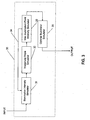
- Fig. 1A illustrates an exemplary brick wall isolation microlithographic mask pattern
- Fig. 1B illustrates an illuminator for imaging that pattern.
- Points on the illuminator of Fig. 1B may be represented by a Cartesian coordinate grid having axes ⁇ s and ⁇ s , and each point on the illuminator may be analyzed for determining an aerial image, or illumination intensity, on the reticle.
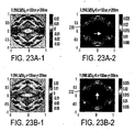
- Figs. 1C-1 and C-2 show the aerial images of X and Y polarization components, respectively, at point 2 on the illuminator of Fig. 1B.
- Figs. 1C-3 and 1C-4 show the aerial images of X and Y polarization components, respectively, at point 4 on the illuminator of Fig. 1B .
- FIGs. 1C-1 and C-2 illustrate aerial images of X polarization at the mask and Y polarization at the mask, respectively, for point 2 ( ⁇ s , 0.78; ⁇ s , 0.46) on the illuminator.
- Y polarization Fig. 1C-2
- Fig. 1C-1 X polarization
- Fig. 1C-1 X polarization
- the overall illumination is optimized resulting in better contrast or resolution over existing systems.
- Each point on the illuminator may be analyzed for determining a polarization state that produces an aerial image with optimal contrast.
- manually analyzing aerial images for a plurality of points of an illuminator in the foregoing manner is rather time-consuming.
- the inventors have devised further novel techniques for optimizing polarized illumination.
- Fig. 2 illustrates a flow diagram of the process employed to optimize illumination intensity in accordance with the present disclosure.
- a cell type e.g. region of the desired mask pattern
- fragmentation points e.g. , points included in the cell
- FIGs. 4A and 16A an exemplary brick wall mask pattern is chosen for the cell, and three fragmentation points 1, 2; and 3 are selected. These points correspond to an end of a line (fragmentation point 1), middle of a line (fragmentation point 2), and a point bridging two lines (fragmentation point 3), respectively.
- Any number of fragmentation points may be chosen for a given cell, and often depends on the complexity of the pattern. For explanation purposes, three fragmentation points were selected and represent global feature types. Of course, the more fragmentation points utilized will increase accuracy of the optimization techniques described herein.
- intensity at each point (x,y) in the wafer plane (image plane) is determined from each point ( ⁇ s , ⁇ s ) in the illuminator plane for each polarization state J x ( ⁇ s , ⁇ s ) and J y ( ⁇ s , ⁇ s ), using the theory of Abbe imaging.
- An expression in terms of I( ⁇ s , ⁇ s ; x, y) may be generated which describes the intensity transfer function at a wafer point (x,y) resulting from the intensity at a illumination point ( ⁇ s , ⁇ s ). Equations for determining intensity in the given manner are known to those of ordinary skill in the art.
- the intensity transfer function, I( ⁇ s , ⁇ s ; x, y) is shown in Equation 3.0 (discussed later).
- Step 22 the Normalized Image Log Slope (NILS) or Image Log Slope (ILS) is determined for each polarization state J x ( ⁇ s , ⁇ s ) and J y ( ⁇ s , ⁇ s ), and at each fragmentation point (x, y).
- w is the normalization factor with units of Length such as CD or ⁇ /NA.
- Equation 3.0 corresponds to I(x,y) applied to Equations 1.0 and 2.0.
- I x ⁇ y ⁇ ⁇ d ⁇ s d ⁇ s ⁇ J x ⁇ s ⁇ ⁇ s ⁇ I xx ⁇ s ⁇ ⁇ s ⁇ x ⁇ y + I yx ⁇ s ⁇ ⁇ s ⁇ x ⁇ y + I zx ⁇ s ⁇ ⁇ s ⁇ x ⁇ y + J y ⁇ s ⁇ ⁇ s ⁇ I xy ⁇ s ⁇ ⁇ s ⁇ x ⁇ y + I yy ⁇ s ⁇ ⁇ s ⁇ x ⁇ y + I yy ⁇ s ⁇ ⁇ s ⁇ x ⁇ y + I zy ⁇ s ⁇ ⁇ s ⁇ x ⁇ y ⁇ ⁇ where:
- Equation 1.0 In order to save space in the following equations (Equations 4.0 and 4.1) for expanding Equation 1.0, (x,y) has omitted for all the intensities, I, and all the electric field components, E, and ( ⁇ s , ⁇ s ) has been omitted for all the illumination intensities Jx and Jy.
- I xx E xx ⁇ E xx * or more generally for intensity and electric field components
- Equations 4.0 and 4.1 may be expanded further in the following manner.
- Pij j is the state of polarization at the object and i is the state of polarization at the image.
- i the state of polarization at the image.
- the transfer function, Pij is given in D. G. Flagello et. al. "Theory of high-NA imaging in homogeneous thin films," J. Opt. Soc. Am. A Vol. 13, No. 1, January 1996, page 53 , and is reproduced below in Equation 6.0.
- optimization constraints are selected, and typically include specifications (or limitations) of the illumination system, such as "Zeiss Specs.” These specifications typically include manufacturing constraints, such as a minimum pupil fill of, for example, 10%, and minimum ring width of, for example, 0.2. It is noted that other optimization constraints may be chosen and are well within the level of one of ordinary skill in the art.
- illumination point intensity and polarization states that maximize the minimum NILS are selected at each fragmentation point (x, y). As set forth below by Equation 7.0, by integrating equation 68, the illumination point intensity and polarization states that maximize the minimum NILS are determined.
- Equation 7.0 max J x ⁇ s ⁇ ⁇ s , J y ⁇ s ⁇ ⁇ s min ILS 1 x ⁇ y , ILS 2 x ⁇ y , ... , ILS n x ⁇ y
- NILS has a direct correlation to exposure latitude or EL.
- the maximum minimum NILS i.e ., the maximum point where slope is 0 or near 0
- NILS is the measure of the image contrast.
- a NILS plot would accurately represent a cross-section of a feature, having vertical edges (slopes of infinity) and horizontal surfaces (slopes of 0). Maximizing the minimum NILS is closest to an ideal feature. Therefore, at each point on the illuminator where NILS is maximized, the aerial image would have the best contrast.
- Step 25 J x ( ⁇ s , ⁇ s ) and J y ( ⁇ s , ⁇ s ) are then summed to determine the optimal illumination to maximize the minimum NILS at each fragmentation point (x, y) at the desired intensity to create an illumination pattern.
- each point on the illuminator is analyzed.
- not all points of an illuminator need to be analyzed, and depends on symmetry of a given pattern. If a given pattern is symmetric about two axes, only a quarter of the illuminator needs to be analyzed. This is seen in the brick wall pattern examples discussed herein. Conversely, if a pattern is symmetric about one axis, only half of the illuminator needs to be analyzed. Moreover, with most, and if not all, patterns, the illuminator will have some kind of symmetry even if a given pattern is not symmetric about X and/or Y axes. In most cases, only half of an illuminator needs to be analyzed.
- an actual illuminator may be created by optimizing each pixel corresponding to each point analyzed above.
- predetermined criteria may be followed for determining which pixel or group of pixels to optimize in accordance with the foregoing techniques.
- predetermined criteria may be followed for determining which pixels or group of pixels to optimize in accordance with the foregoing techniques.
- predetermined criteria would likely depend on the type of illuminator, scanner, etc., and given pattern.
- Fig. 3 illustrates a computer system 30 adapted for optimizing illumination as described above.
- the computer system includes an illumination simulator 31 for determining intensity at each point on an illuminator for each polarization state. Based on the illumination and polarization states, Image Log Slope Simulator 32 generates an ILS or NILS. Max Illumination Point Intensity Simulator 33 maximizes minimum ILS or NILS based on the output of ILS Simulator 32. A feedback path 34 is provided for prompting calculations for each point on the illuminator. Finally, Optimal Illuminator Simulator 35 creates an optimum illuminator based on calculation representing each point of the illuminator.
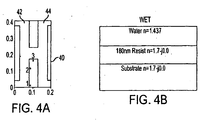
- a brick wall isolation pattern 40 for a 0.4 nm by 0.2 nm section of a microlithographic mask is illustrated. Illustrated further are three fragmentation points, denoted by numerals 1, 2 and 3. As mentioned above, fragmentation point 1 corresponds to the end of the line feature 42 of the brick wall pattern 40; fragmentation point 2 corresponds to a mid-point of the line feature 42; and fragmentation point 3 corresponds to a connection of lines 42 and 44.
- Fig. 4B illustrates wafer topography for an immersion system to which the brick wall pattern 40 of Fig. 4A was applied.
- An illumination system (described below) was used having a wavelength, ⁇ , of 193nm and a numerical aperture, NA, of 1.2.
- Figs. 5A-1 through A-3 and 5B-1 through B-3 illustrate a simulation representing the transfer of the projection pupil to the substrate.
- an illumination at the mask having X polarization may influence other polarization states at the wafer. This can be represented by the following equation.
- Pij The transfer function, Pij, is given in D. G. Flagello et. al. "Theory of high-NA imaging in homogeneous thin films," J. Opt. Soc. Am. A Vol. 13, No. 1, January 1996, page 53 . Pij is shown below.
- P xx P xy P yx P yy P zx P zy F s F p 0 0 0 0 F s F p 0 0 0 0 F zp ⁇ P xxs P yxs P xxp P yxp P xys P yys P xyp P yyp P xzp P yzp
- Figs. 5A-1 - 5A-3 illustrate simulations for X polarization at the mask (Mask Ex), and polarization states at the wafer (Wafer Ex, Wafer Ey, and Wafer Ez, respectively).
- Figs. 5B-1 - 5B-1 illustrate simulations for Y polarization at the mask (Mask Ey), and polarization states at the wafer (Wafer Ex, Wafer Ey, and Wafer Ez, respectively).
- polarization Mask Ex and Wafer Ex Fig. 5A-1
- polarization Mask Ey and Wafer Ey Fig. 5B-2
- Fig. 5B-2 illustrate states in which optimal contrast can be accomplished.
- Fig. 6 illustrates the corresponding contour plot and illumination intensity for an optimized unpolarized state.
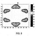
- Figs. 7 and 8 illustrate corresponding contour plots and illumination intensity for optimized polarized state and optimized TE polarized state, respectively.
- optimized polarization Fig. 7
- optimized TE polarization Fig. 8
- greater illumination is represented by the expansiveness of the plot found along the poles in Figs. 7 & 8 when compared against the plot for Fig. 6 .
- Figs. 7 and 8 further illustrate the state of polarization defined by the plurality of polarization vectors 70 of Fig. 7 and the plurality of polarization vectors 80 of Fig. 8 .
- the polarization vectors 70, 80 at certain corresponding points on the illuminator, only Y polarization is desirable and on other points only X polarization is desirable. Comparing Fig. 7 to Fig. 8 , polarization vectors 70 change more abruptly than polarization vectors 80. This abrupt change is more desirable, as it improves image contrast.
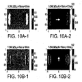
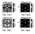
- Figs. 9-11 illustrate illumination pupils NILS response plots at points 1, 2, and 3, respectively, on the brick wall pattern of Fig. 4A .
- Subfigures A-1 and A-2 of Figs. 9-11 show NILS response plots at these points for X polarization
- subfigures B-1 and B-2 show NILS response plots at these points for Y polarization.
- comparison of X and Y polarization shows that Y polarization has better illumination.
- illumination intensity for Y polarization ( Figs. 9B-1 and B-2 ) show approximately a 300% improvement over X polarization.
- intensity levels 90 are far less than intensity levels 92.
- use of Y polarization over X polarization dramatically improves illumination intensity.
- Fig. 10 illustrates corresponding pupil NILS response plots.
- Y polarization has approximately a 300% improvement over X polarization shown by comparison intensity representation 100 and intensity representation 102.
- fragmentation point 3 ( Fig. 11 ) by comparing intensity levels at 110 with those at 112, X polarization has a 40% improvement over Y polarization.
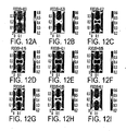
- Figs. 12-14 show simulation of the print of the brick wall pattern of Fig. 4A with wafer topography of Fig. 4B for optimized unpolarized illumination, optimized polarized illumination and optimized TE polarized illumination, respectively.
- Aerial images from a focus of -0.3 to a focus of 0.1 at increments of 0.05, respectively, are shown by subfigures A-I for Figs. 12-14 .
- Each subfigure shows an aerial image of the brick wall and the resist through focus.
- a focus of -0.1 Figs. 12E , 13E and 14E
- a focus of -0.1 tends to illustrate the brick wall having the best contrast.
- Figs. 15A-15C illustrate ILS plots through focus for fragmentation points 1, 2 and 3 of the brick wall of Fig. 4A for unpolarized illumination, polarized illumination and TE polarized illumination, respectively.
- polarization illumination may be optimized.
- Plots of Figs. 15A-15C illustrate this unique feature. Specifically, at fragmentation point 1 ( Fig. 15A ), polarized illumination has the maximum ILS, while unpolarized illumination has the minimum ILS. TE polarized illumination falls in between. The same is true for fragmentation point 2 ( Fig. 15B ) and for fragmentation point 3 ( Fig. 15C ). In other words, the lowest image log slope corresponds to the unpolarized case and the highest image log slope corresponds to the polarized case.
- a higher image log slope results in a higher contrast, which in turn provides increased exposure latitude and a better process window. Therefore, by optimizing polarization at each fragmentation point as described above, determined in accordance with the flow diagram of Fig. 1 , a higher process window may be obtained.
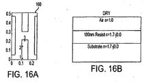
- Fig. 16A illustrates a half-pitch brick wall isolation pattern 160 for a 0.4 nm by 0.2 nm section of a microlithographic mask having three fragmentation points, denoted by numerals 1, 2 and 3.
- Fig. 16B however illustrates wafer topography for a dry system to which the brick wall pattern 160 of Fig. 16A will be applied.
- transmittance of air is 1.
- an illumination system (described below) was used having a wavelength, ⁇ , of 193nm and a numerical aperture, NA, of 1.2.
- Figs. 17A1-A3and B1-B8 are the same as that illustrated by Fig. 5 . Accordingly, projection pupils remain the same regardless of whether the wafer is immersed in water or dry. Description of this figure will not be repeated for the sake of conciseness.
- Fig. 18 illustrates the corresponding contour plot and illumination intensity for an optimized unpolarized state.
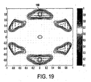
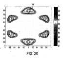
- Figs. 19 and 20 illustrate corresponding contour plots and illumination intensity for optimized polarized state and optimized TE polarized state, respectively.
- optimized polarization Fig. 19
- optimized TE polarization Fig. 20
- Figs. 19 and 20 illustrate further states of polarization defined by the plurality of polarization vectors 190 of Fig. 19 and the plurality of polarization vectors 200 of Fig. 20 .
- polarization vectors 190, 200 As shown by the polarization vectors 190, 200, at certain points on the illuminator, only Y polarization is desirable, and on other points, only X polarization is desirable. As before, polarization vectors 190 change more abruptly than do polarization vectors 200, and are therefore more desirable and give a better contrast.
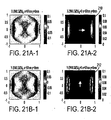
- Figs. 21-23 illustrate illumination pupils NILS response plots at points 1, 2, and 3, respectively, on the brick wall pattern of Fig. 16A .
- Subfigures A-1 and A-2 of Figs. 21-23 show NILS response plots at these points for X polarization
- subfigures B-1 and B-2 show NILS response plots at these points for Y polarization.
- comparison of X and Y polarization shows greater illumination for X polarization.
- illumination intensity for Y polarization ( Figs. 21B-1 and B-2 ) show approximately a 50% improvement over X polarization.
- comparison of intensity levels 212 show a 50% improvement over the intensity levels 210.
- use of Y polarization over X polarization improves illumination intensity.
- Fig. 22 illustrates corresponding pupil NILS response plots.
- Y polarization has a 50% improvement over X polarization shown by comparison intensity levels 220 and intensity levels 222.
- X polarization has a 40% improvement over Y polarization.
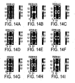
- Figs. 24-26 show simulation of the print of the brick wall pattern of Fig. 16A with the wafer topography of Fig. 16B for optimized unpolarized illumination, optimized polarized illumination and optimized TE polarized illumination, respectively.
- Aerial images from a focus of -0.3 to a focus of 0.1 at increments of 0.05, respectively, are shown by subfigures A-I of each of Figs. 24-26 .
- Each subfigure shows an aerial image of the brick wall and the resist through focus.
- a focus of -0.1 Figs. 24E , 25E and 26E
- a focus of -0.1 tends to illustrate the brick wall at the highest contrast.
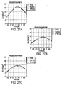
- Figs. 27A-C illustrate ILS plots through focus for fragmentation points 1, 2 and 3 of the brick wall of Fig. 16A for unpolarized illumination, polarized illumination and TE polarized illumination, respectively.
- polarization illumination may be optimized.
- TE azimuthal illumination has the maximum ILS
- unpolarized illumination has the minimum ILS.
- fragmentation point 3 Fig. 27C
- optimized polarization improves ILS by approximately 15% over unpolarized illumination.
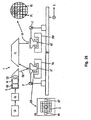
- Fig. 28 schematically depicts a lithographic projection apparatus suitable for use with a mask designed with the aid of the current invention.
- the apparatus comprises:
- the apparatus is of a transmissive type (i.e., has a transmissive mask). However, in general, it may also be of a reflective type, for example (with a reflective mask). Alternatively, the apparatus may employ another kind of patterning means as an alternative to the use of a mask; examples include a programmable mirror array or LCD matrix.
- the source LA (e.g ., a mercury lamp or excimer laser) produces a beam of radiation.
- This beam is fed into an illumination system (illuminator) IL, either directly or after having traversed conditioning means, such as a beam expander Ex, for example.
- the illuminator IL may comprise adjusting means AM for setting the outer and/or inner radial extent (commonly referred to as ⁇ -outer and ⁇ -inner, respectively) of the intensity distribution in the beam.
- ⁇ -outer and ⁇ -inner commonly referred to as ⁇ -outer and ⁇ -inner, respectively
- it will generally comprise various other components, such as an integrator IN and a condenser CO.
- the beam PB impinging on the mask MA has a desired uniformity and intensity distribution in its cross-section.
- the source LA may be within the housing of the lithographic projection apparatus (as is often the case when the source LA is a mercury lamp, for example), but that it may also be remote from the lithographic projection apparatus, the radiation beam that it produces being led into the apparatus ( e.g. , with the aid of suitable directing mirrors); this latter scenario is often the case when the source LA is an excimer laser (e.g. , based on KrF, ArF or F 2 lasing).
- the current invention encompasses at least both of these scenarios.
- the beam PB subsequently intercepts the mask MA, which is held on a mask table MT. Having traversed the mask MA, the beam PB passes through the lens PL, which focuses the beam PB onto a target portion C of the substrate W. With the aid of the second positioning means (and interferometric measuring means IF), the substrate table WT can be moved accurately, e.g . so as to position different target portions C in the path of the beam PB. Similarly, the first positioning means can be used to accurately position the mask MA with respect to the path of the beam PB, e.g., after mechanical retrieval of the mask MA from a mask library, or during a scan.
- the mask table MT may just be connected to a short stroke actuator, or may be fixed.
- the depicted tool can be used in two different modes:
- the concepts disclosed herein may simulate or mathematically model any generic imaging system for imaging sub wavelength features, and may be especially useful with emerging imaging technologies capable of producing wavelengths of an increasingly smaller size.
- Emerging technologies already in use include EUV (extreme ultra violet) lithography that is capable of producing a 193nm wavelength with the use of a ArF laser, and even a 157nm wavelength with the use of a Fluorine laser.
- EUV lithography is capable of producing wavelengths within a range of 20-5nm by using a synchrotron or by hitting a material (either solid or a plasma) with high energy electrons in order to produce photons within this range.
- illumination may be produced by reflective mirrors with a multi-stack of Molybdenum and Silicon.
- the multi-stack mirror has a 40 layer pairs of Molybdenum and Silicon where the thickness of each layer is a quarter wavelength. Even smaller wavelengths may be produced with X-ray lithography.
- a synchrotron is used to produce an X-ray wavelength. Since most material is absorptive at x-ray wavelengths, a thin piece of absorbing material defines where features would print (positive resist) or not print (negative resist).
- Software functionalities of a computer system involve programming, including executable code, may be used to implement the above described imaging model.
- the software code is executable by the general-purpose computer.
- the code and possibly the associated data records are stored within a general-purpose computer platform.
- the software may be stored at other locations and/or transported for loading into the appropriate general-purpose computer systems.
- the embodiments discussed above involve one or more software products in the form of one or more modules of code carried by at least one machine-readable medium. Execution of such code by a processor of the computer system enables the platform to implement the catalog and/or software downloading functions, in essentially the manner performed in the embodiments discussed and illustrated herein.
- Non-volatile media include, for example, optical or magnetic disks, such as any of the storage devices in any computer(s) operating as one of the server platform, discussed above.
- Volatile media include dynamic memory, such as main memory of such a computer platform.
- Physical transmission media include coaxial cables; copper wire and fiber optics, including the wires that comprise a bus within a computer system.
- Carrier-wave transmission media can take the form of electric or electromagnetic signals, or acoustic or light waves such as those generated during radio frequency (RF) and infrared (IR) data communications.
- Common forms of computer-readable media therefore include, for example: a floppy disk, a flexible disk, hard disk, magnetic tape, any other magnetic medium, a CD-ROM, DVD, any other optical medium, less commonly used media such as punch cards, paper tape, any other physical medium with patterns of holes, a RAM, a PROM, and EPROM, a FLASH-EPROM, any other memory chip or cartridge, a carrier wave transporting data or instructions, cables or links transporting such a carrier wave, or any other medium from which a computer can read programming code and/or data.
- Many of these forms of computer readable media may be involved in carrying one or more sequences of one or more instructions to a processor for execution.
Landscapes
- Physics & Mathematics (AREA)
- General Physics & Mathematics (AREA)
- Exposure And Positioning Against Photoresist Photosensitive Materials (AREA)
- Exposure Of Semiconductors, Excluding Electron Or Ion Beam Exposure (AREA)
- Polarising Elements (AREA)
Claims (10)
- Ein Verfahren zum Optimieren der Polarisation einer Beleuchtung eines Musters, das in einer Oberfläche eines Substrats zu bilden ist, wobei die Beleuchtung aus einer Beleuchterebene stammt, die individuelle Pixel beinhaltet, von wo Licht das Muster beleuchtet, um über ein Projektionssystem in die Oberfläche des Substrats projiziert zu werden, wobei das Verfahren die folgenden Schritte beinhaltet:(a) Auswählen einer Vielzahl von Fragmentierungspunkten in dem Muster;(b) Bestimmen einer Beleuchtungsintensität für mindestens ein Pixel in einer Beleuchterebene für mindestens zwei Polarisationszustände;(c) Bestimmen einer Bild-Log-Steigung an den Fragmentierungspunkten auf Substratniveau für das mindestens eine Pixel auf der Beleuchterebene für die mindestens zwei Polarisationszustände;(d) Bestimmen einer minimalen Bild-Log-Steigung (ILS) an den Fragmentierungspunkten für jeden der mindestens zwei Polarisationszustände;(e) Auswählen eines optimalen Polarisationszustandes für das mindestens eine Pixel in der Beleuchterebene, der die minimale ILS maximiert; und(f) Wiederholen der Schritte (a) bis (e) für jedes einer Vielzahl von Pixeln in der Beleuchterebene.
- Verfahren gemäß Anspruch 1, wobei Schritt (f) die Schritte (a) bis (e) für jedes einer Vielzahl von Pixeln in einem Teil der Beleuchterebene abhängig von einer Symmetrie des Musters wiederholt.
- Verfahren gemäß Anspruch 1, wobei Schritt (f) die Schritte (a) bis (e) für jedes einer Vielzahl von Pixeln in einer Hälfte der Beleuchterebene wiederholt.
- Verfahren gemäß Anspruch 2 oder 3, das ferner den Schritt des Kombinierens der optimalen Polarisation für jedes der Vielzahl von Pixeln in der Beleuchterebene zum Erzeugen einer optimalen polarisierten Beleuchtung des Musters beinhaltet.
- Verfahren gemäß einem der vorhergehenden Ansprüche, wobei der optimale Polarisationszustand eine Kombination der mindestens zwei Polarisationszustände ist.
- Verfahren gemäß einem der vorhergehenden Ansprüche, wobei der optimale Polarisationszustand einem der mindestens zwei Polarisationszustände entspricht.
- Verfahren gemäß einem der vorhergehenden Ansprüche, wobei die mindestens zwei Polarisationszustände mindestens X- und Y-Polarisationszustände umfassen.
- Ein Computerprogrammprodukt, das einen ausführbaren Code beinhaltet, der durch mindestens ein maschinenlesbares Medium transportierbar ist, wobei eine Ausführung des Codes durch mindestens einen programmierbaren Computer bewirkt, dass der mindestens eine programmierbare Computer ein Verfahren gemäß einem der vorhergehenden Ansprüche durchführt.
- Ein Verfahren zum Herstellen einer Vorrichtung, das das Bestimmen einer Optimalpolarisation der Beleuchtung eines Musters gemäß dem Verfahren nach einem der Ansprüche 1 bis 7, das Beleuchten des Musters im Wesentlichen unter Verwendung der Optimalpolarisation, das Projizieren eines Bildes des Musters auf ein Substrat beinhaltet.
- Ein Gerät zum Abbilden eines Maskenmusters auf einem Zielabschnitt eines Substrats unter Verwendung von optimierter polarisierter Beleuchtung zum Vergrößern des Prozessfensters, wobei das Gerät Folgendes beinhaltet:ein Strahlungssystem zum Zuführen eines Projektionsstrahls aus polarisierter Strahlung;einen Beleuchter zum Empfangen des Projektionsstrahls aus Strahlung und Projizieren eines angepassten Strahls aus Strahlung auf einen Abschnitt einer Maske, wobei die von dem Beleuchter emittierte Beleuchtung aus einer Beleuchterebene stammt, die individuelle Pixel beinhaltet, von wo Licht das Maskenmuster beleuchtet, um über ein Projektionssystem in die Oberfläche des Substrats projiziert zu werden; unddas Projektionssystem zum Abbilden eines entsprechenden bestrahlten Abschnitts einer Maske auf den Zielabschnitt des Substrats, wobei das Gerät ferner ein Computersystem beinhaltet, das konfiguriert ist, um die Polarisation und Intensität an jedem der Vielzahl von Pixeln durch das Durchführen der folgenden Schritte zu optimieren:wobei(a) Auswählen einer Vielzahl von Fragmentierungspunkten in dem Muster;(b) Bestimmen einer Beleuchtungsintensität für mindestens ein Pixel in einer Beleuchterebene für mindestens zwei Polarisationszustände;(c) Bestimmen einer Bild-Log-Steigung an dem Fragmentierungspunkt für das mindestens eine Pixel in der Beleuchterebene für die mindestens zwei Polarisationszustände;(d) Bestimmen einer minimalen Bild-Log-Steigung (ILS) an den Fragmentierungspunkten für jeden der mindestens zwei Polarisationszustände;(e) Auswählen eines optimalen Polarisationszustandes für das mindestens eine Pixel in der Beleuchterebene, der die minimale ILS maximiert; und(f) Wiederholen der Schritte (a) bis (e) für jedes der Vielzahl von Pixeln in der Beleuchterebene;
der Beleuchter an der Vielzahl von Pixeln angepasst ist, um die Polarisation und Intensität an jedem der Vielzahl von Pixeln zu optimieren.
Applications Claiming Priority (2)
| Application Number | Priority Date | Filing Date | Title |
|---|---|---|---|
| US53066203P | 2003-12-19 | 2003-12-19 | |
| US530662P | 2003-12-19 |
Publications (3)
| Publication Number | Publication Date |
|---|---|
| EP1544679A2 EP1544679A2 (de) | 2005-06-22 |
| EP1544679A3 EP1544679A3 (de) | 2007-07-25 |
| EP1544679B1 true EP1544679B1 (de) | 2014-01-08 |
Family
ID=34520284
Family Applications (1)
| Application Number | Title | Priority Date | Filing Date |
|---|---|---|---|
| EP04257019.2A Ceased EP1544679B1 (de) | 2003-12-19 | 2004-11-12 | Optimierte Beleuchtung mit polarisiertem Licht |
Country Status (7)
| Country | Link |
|---|---|
| US (3) | US7292315B2 (de) |
| EP (1) | EP1544679B1 (de) |
| JP (1) | JP4491332B2 (de) |
| KR (1) | KR100919856B1 (de) |
| CN (1) | CN100524028C (de) |
| SG (1) | SG135042A1 (de) |
| TW (1) | TWI373278B (de) |
Families Citing this family (28)
| Publication number | Priority date | Publication date | Assignee | Title |
|---|---|---|---|---|
| US7292315B2 (en) * | 2003-12-19 | 2007-11-06 | Asml Masktools B.V. | Optimized polarization illumination |
| US8270077B2 (en) | 2004-01-16 | 2012-09-18 | Carl Zeiss Smt Gmbh | Polarization-modulating optical element |
| US20070019179A1 (en) | 2004-01-16 | 2007-01-25 | Damian Fiolka | Polarization-modulating optical element |
| CN101793993B (zh) | 2004-01-16 | 2013-04-03 | 卡尔蔡司Smt有限责任公司 | 光学元件、光学布置及系统 |
| US7324280B2 (en) | 2004-05-25 | 2008-01-29 | Asml Holding N.V. | Apparatus for providing a pattern of polarization |
| WO2005122218A1 (ja) * | 2004-06-09 | 2005-12-22 | Nikon Corporation | 露光装置及びデバイス製造方法 |
| JP4528580B2 (ja) * | 2004-08-24 | 2010-08-18 | 株式会社東芝 | 照明光源の設計方法、マスクパターン設計方法、フォトマスクの製造方法、半導体装置の製造方法、及びプログラム |
| US7317506B2 (en) * | 2005-03-29 | 2008-01-08 | Asml Netherlands B.V. | Variable illumination source |
| US7548302B2 (en) * | 2005-03-29 | 2009-06-16 | Asml Netherlands B.V. | Lithographic apparatus and device manufacturing method |
| US20100215273A1 (en) * | 2005-06-24 | 2010-08-26 | Koninklijke Philips Electronics, N.V. | Methods and devices for characterizing polarization of illumination system |
| US7804646B2 (en) * | 2006-01-31 | 2010-09-28 | Asml Masktools B.V. | Method for decomposition of a customized DOE for use with a single exposure into a set of multiple exposures using standard DOEs with optimized exposure settings |
| US7548315B2 (en) * | 2006-07-27 | 2009-06-16 | Asml Netherlands B.V. | System and method to compensate for critical dimension non-uniformity in a lithography system |
| US7705998B2 (en) * | 2007-09-12 | 2010-04-27 | Infineon Technologies Ag | Method for evaluating an optical imaging process |
| JP2009071125A (ja) * | 2007-09-14 | 2009-04-02 | Canon Inc | 露光条件を決定する方法及びプログラム |
| US7673278B2 (en) * | 2007-11-29 | 2010-03-02 | Tokyo Electron Limited | Enhanced process yield using a hot-spot library |
| TW200938957A (en) * | 2008-03-05 | 2009-09-16 | Nanya Technology Corp | Feedback system and feedback method for controlling power ratio of light source |
| JP2009251521A (ja) * | 2008-04-10 | 2009-10-29 | Jedat Inc | ガラスデータ設計システム、方法およびプログラム |
| JP5607327B2 (ja) * | 2009-08-27 | 2014-10-15 | キヤノン株式会社 | 決定方法、露光方法、デバイスの製造方法及びプログラム |
| NL2005738A (en) | 2009-12-15 | 2011-06-16 | Asml Holding Nv | Improved polarization designs for lithographic apparatus. |
| NL2007303A (en) * | 2010-09-23 | 2012-03-26 | Asml Netherlands Bv | Process tuning with polarization. |
| NL2007306A (en) | 2010-09-23 | 2012-03-26 | Asml Netherlands Bv | Source polarization optimization. |
| JP2012099596A (ja) * | 2010-11-01 | 2012-05-24 | Panasonic Corp | 照明形状の最適化方法、マスク形状の最適化方法及びパターン形成方法 |
| JP2012169483A (ja) * | 2011-02-15 | 2012-09-06 | Toshiba Corp | 露光条件決定プログラム |
| CN106028585B (zh) * | 2016-05-23 | 2018-03-09 | 电子科技大学 | 一种基于牛顿极值搜索算法的双闭环照明节能控制方法 |
| CN106028584B (zh) * | 2016-05-23 | 2018-03-09 | 电子科技大学 | 一种基于梯度极值搜索算法的双闭环照明节能控制方法 |
| CN106341938B (zh) * | 2016-11-07 | 2018-08-07 | 电子科技大学 | 基于变幅值牛顿极值搜索算法的照明节能控制方法 |
| EP3336608A1 (de) * | 2016-12-16 | 2018-06-20 | ASML Netherlands B.V. | Verfahren und vorrichtung für bildanalyse |
| DE102017115262B9 (de) * | 2017-07-07 | 2021-05-27 | Carl Zeiss Smt Gmbh | Verfahren zur Charakterisierung einer Maske für die Mikrolithographie |
Family Cites Families (22)
| Publication number | Priority date | Publication date | Assignee | Title |
|---|---|---|---|---|
| US4985579A (en) | 1989-10-16 | 1991-01-15 | Dow Corning Corporation | Removal of hydrogen-containing silanes from organosilane mixtures |
| US6404482B1 (en) * | 1992-10-01 | 2002-06-11 | Nikon Corporation | Projection exposure method and apparatus |
| JP3339593B2 (ja) | 1993-04-22 | 2002-10-28 | 株式会社ニコン | 投影露光装置、及び該装置を用いた素子製造方法 |
| KR0173168B1 (ko) * | 1994-02-24 | 1999-03-20 | 가네꼬 히사시 | 웨이퍼상의 레지스트막을 노광하기 위한 노광계와 그에 사용되는 조명계 및 방법 |
| DE19535392A1 (de) * | 1995-09-23 | 1997-03-27 | Zeiss Carl Fa | Radial polarisationsdrehende optische Anordnung und Mikrolithographie-Projektionsbelichtungsanlage damit |
| EP0824722B1 (de) * | 1996-03-06 | 2001-07-25 | Asm Lithography B.V. | Differential-interferometer-system und lithographischer "step and scan" apparat ausgestattet mit diesem system |
| WO1998028665A1 (en) * | 1996-12-24 | 1998-07-02 | Koninklijke Philips Electronics N.V. | Two-dimensionally balanced positioning device with two object holders, and lithographic device provided with such a positioning device |
| US6140660A (en) | 1999-03-23 | 2000-10-31 | Massachusetts Institute Of Technology | Optical synthetic aperture array |
| US6491396B2 (en) * | 2000-02-15 | 2002-12-10 | Seiko Epson Corporation | Projector modulating a plurality of partial luminous fluxes according to imaging information by means of an electro-optical device |
| US6563566B2 (en) * | 2001-01-29 | 2003-05-13 | International Business Machines Corporation | System and method for printing semiconductor patterns using an optimized illumination and reticle |
| US7396558B2 (en) * | 2001-01-31 | 2008-07-08 | Toray Industries, Inc. | Integrated mask and method and apparatus for manufacturing organic EL device using the same |
| TWI285295B (en) * | 2001-02-23 | 2007-08-11 | Asml Netherlands Bv | Illumination optimization in lithography |
| US6519760B2 (en) * | 2001-02-28 | 2003-02-11 | Asml Masktools, B.V. | Method and apparatus for minimizing optical proximity effects |
| JP2005507093A (ja) * | 2001-10-19 | 2005-03-10 | スリーエム イノベイティブ プロパティズ カンパニー | 照明偏光変換システム |
| US7293249B2 (en) * | 2002-01-31 | 2007-11-06 | Juan Andres Torres Robles | Contrast based resolution enhancement for photolithographic processing |
| US6888615B2 (en) * | 2002-04-23 | 2005-05-03 | Asml Holding N.V. | System and method for improving linewidth control in a lithography device by varying the angular distribution of light in an illuminator as a function of field position |
| JP2004111579A (ja) * | 2002-09-17 | 2004-04-08 | Canon Inc | 露光方法及び装置 |
| US7090964B2 (en) | 2003-02-21 | 2006-08-15 | Asml Holding N.V. | Lithographic printing with polarized light |
| DE602004032449D1 (de) * | 2003-09-17 | 2011-06-09 | Photonic Lattice Inc | Polarisations-Analysegerät und entsprechende Methode |
| TW201834020A (zh) * | 2003-10-28 | 2018-09-16 | 日商尼康股份有限公司 | 照明光學裝置、曝光裝置、曝光方法以及元件製造方法 |
| KR20050043713A (ko) | 2003-11-05 | 2005-05-11 | 에이에스엠엘 마스크툴즈 비.브이. | 고유 분해 기반 opc 모델 |
| US7292315B2 (en) * | 2003-12-19 | 2007-11-06 | Asml Masktools B.V. | Optimized polarization illumination |
-
2004
- 2004-08-20 US US10/921,878 patent/US7292315B2/en not_active Expired - Fee Related
- 2004-11-09 SG SG200406521-5A patent/SG135042A1/en unknown
- 2004-11-11 KR KR1020040091966A patent/KR100919856B1/ko not_active Expired - Fee Related
- 2004-11-11 JP JP2004327534A patent/JP4491332B2/ja not_active Expired - Fee Related
- 2004-11-12 TW TW093134767A patent/TWI373278B/zh not_active IP Right Cessation
- 2004-11-12 EP EP04257019.2A patent/EP1544679B1/de not_active Ceased
- 2004-11-12 CN CNB2004100947120A patent/CN100524028C/zh not_active Expired - Fee Related
-
2007
- 2007-10-16 US US11/907,648 patent/US7710544B2/en not_active Expired - Fee Related
-
2010
- 2010-05-04 US US12/773,775 patent/US8395757B2/en not_active Expired - Lifetime
Also Published As
| Publication number | Publication date |
|---|---|
| US20050134822A1 (en) | 2005-06-23 |
| TWI373278B (en) | 2012-09-21 |
| SG135042A1 (en) | 2007-09-28 |
| EP1544679A2 (de) | 2005-06-22 |
| US7292315B2 (en) | 2007-11-06 |
| TW200527953A (en) | 2005-08-16 |
| KR20050062364A (ko) | 2005-06-23 |
| EP1544679A3 (de) | 2007-07-25 |
| US20080043215A1 (en) | 2008-02-21 |
| US7710544B2 (en) | 2010-05-04 |
| JP4491332B2 (ja) | 2010-06-30 |
| JP2005183938A (ja) | 2005-07-07 |
| CN1629731A (zh) | 2005-06-22 |
| KR100919856B1 (ko) | 2009-09-30 |
| CN100524028C (zh) | 2009-08-05 |
| US20110051114A1 (en) | 2011-03-03 |
| US8395757B2 (en) | 2013-03-12 |
Similar Documents
| Publication | Publication Date | Title |
|---|---|---|
| EP1544679B1 (de) | Optimierte Beleuchtung mit polarisiertem Licht | |
| US7594199B2 (en) | Method of optical proximity correction design for contact hole mask | |
| US10657641B2 (en) | Source and mask optimization by changing intensity and shape of the illumination source and magnitude and phase of mask diffraction orders | |
| US7016017B2 (en) | Lithographic apparatus and method for optimizing an illumination source using isofocal compensation | |
| US7180576B2 (en) | Exposure with intensity balancing to mimic complex illuminator shape | |
| KR100961686B1 (ko) | 모델-기반 스캐너 튜닝을 수행하는 방법 | |
| US7349066B2 (en) | Apparatus, method and computer program product for performing a model based optical proximity correction factoring neighbor influence | |
| JP5121117B2 (ja) | 強度プロフィールを最適化する方法及びプログラム | |
| US9053280B2 (en) | Rule optimization in lithographic imaging based on correlation of functions representing mask and predefined optical conditions | |
| EP1630617B1 (de) | Methode zur Optimierung des diffraktiven optischen Elements (DOE) zum Abgleich des optischen Naheffekts (OPE) zwischen verschiedenen Lithographiesystemen | |
| EP1560073A2 (de) | Methode zur Vorhersage und zur Minimierung von Abweichungen vom OPC Modell die durch Kombination/Anpassung verschiedener Belichtungsgeräte hervorgerufen werden unter Benützung eines kalibrierten Eigenfunktionszerlegungsmodells | |
| US7034919B2 (en) | Method and apparatus for providing lens aberration compensation by illumination source optimization | |
| US8043797B2 (en) | Lithographic apparatus and device manufacturing method | |
| TW202240316A (zh) | 依據微影設備或製程特徵所特徵化之表示選擇圖案 | |
| KR20240058872A (ko) | 계측 데이터로부터의 소스 분리 |
Legal Events
| Date | Code | Title | Description |
|---|---|---|---|
| PUAI | Public reference made under article 153(3) epc to a published international application that has entered the european phase |
Free format text: ORIGINAL CODE: 0009012 |
|
| AK | Designated contracting states |
Kind code of ref document: A2 Designated state(s): AT BE BG CH CY CZ DE DK EE ES FI FR GB GR HU IE IS IT LI LU MC NL PL PT RO SE SI SK TR |
|
| AX | Request for extension of the european patent |
Extension state: AL HR LT LV MK YU |
|
| PUAL | Search report despatched |
Free format text: ORIGINAL CODE: 0009013 |
|
| AK | Designated contracting states |
Kind code of ref document: A3 Designated state(s): AT BE BG CH CY CZ DE DK EE ES FI FR GB GR HU IE IS IT LI LU MC NL PL PT RO SE SI SK TR |
|
| AX | Request for extension of the european patent |
Extension state: AL HR LT LV MK YU |
|
| 17P | Request for examination filed |
Effective date: 20080104 |
|
| AKX | Designation fees paid |
Designated state(s): DE FR GB IT NL |
|
| 17Q | First examination report despatched |
Effective date: 20090417 |
|
| GRAP | Despatch of communication of intention to grant a patent |
Free format text: ORIGINAL CODE: EPIDOSNIGR1 |
|
| GRAS | Grant fee paid |
Free format text: ORIGINAL CODE: EPIDOSNIGR3 |
|
| GRAP | Despatch of communication of intention to grant a patent |
Free format text: ORIGINAL CODE: EPIDOSNIGR1 |
|
| INTG | Intention to grant announced |
Effective date: 20130712 |
|
| GRAA | (expected) grant |
Free format text: ORIGINAL CODE: 0009210 |
|
| AK | Designated contracting states |
Kind code of ref document: B1 Designated state(s): DE FR GB IT NL |
|
| REG | Reference to a national code |
Ref country code: GB Ref legal event code: FG4D |
|
| REG | Reference to a national code |
Ref country code: DE Ref legal event code: R096 Ref document number: 602004044174 Country of ref document: DE Effective date: 20140220 |
|
| REG | Reference to a national code |
Ref country code: NL Ref legal event code: VDEP Effective date: 20140108 |
|
| PG25 | Lapsed in a contracting state [announced via postgrant information from national office to epo] |
Ref country code: NL Free format text: LAPSE BECAUSE OF FAILURE TO SUBMIT A TRANSLATION OF THE DESCRIPTION OR TO PAY THE FEE WITHIN THE PRESCRIBED TIME-LIMIT Effective date: 20140108 |
|
| REG | Reference to a national code |
Ref country code: DE Ref legal event code: R097 Ref document number: 602004044174 Country of ref document: DE |
|
| PLBE | No opposition filed within time limit |
Free format text: ORIGINAL CODE: 0009261 |
|
| STAA | Information on the status of an ep patent application or granted ep patent |
Free format text: STATUS: NO OPPOSITION FILED WITHIN TIME LIMIT |
|
| REG | Reference to a national code |
Ref country code: DE Ref legal event code: R081 Ref document number: 602004044174 Country of ref document: DE Owner name: ASML NETHERLANDS B.V., NL Free format text: FORMER OWNER: ASML MASKTOOLS B.V., VELDHOVEN, NL Effective date: 20141016 Ref country code: DE Ref legal event code: R081 Ref document number: 602004044174 Country of ref document: DE Owner name: ASML NETHERLANDS B.V., NL Free format text: FORMER OWNER: ASML MASKTOOLS B.V., VELDHOVEN, NL Effective date: 20140114 |
|
| 26N | No opposition filed |
Effective date: 20141009 |
|
| REG | Reference to a national code |
Ref country code: FR Ref legal event code: TP Owner name: ASML NETHERLANDS B.V., NL Effective date: 20141209 |
|
| REG | Reference to a national code |
Ref country code: DE Ref legal event code: R097 Ref document number: 602004044174 Country of ref document: DE Effective date: 20141009 |
|
| GBPC | Gb: european patent ceased through non-payment of renewal fee |
Effective date: 20141112 |
|
| PG25 | Lapsed in a contracting state [announced via postgrant information from national office to epo] |
Ref country code: GB Free format text: LAPSE BECAUSE OF NON-PAYMENT OF DUE FEES Effective date: 20141112 |
|
| REG | Reference to a national code |
Ref country code: FR Ref legal event code: PLFP Year of fee payment: 12 |
|
| PG25 | Lapsed in a contracting state [announced via postgrant information from national office to epo] |
Ref country code: IT Free format text: LAPSE BECAUSE OF FAILURE TO SUBMIT A TRANSLATION OF THE DESCRIPTION OR TO PAY THE FEE WITHIN THE PRESCRIBED TIME-LIMIT Effective date: 20140108 |
|
| REG | Reference to a national code |
Ref country code: FR Ref legal event code: PLFP Year of fee payment: 13 |
|
| REG | Reference to a national code |
Ref country code: FR Ref legal event code: PLFP Year of fee payment: 14 |
|
| PGFP | Annual fee paid to national office [announced via postgrant information from national office to epo] |
Ref country code: FR Payment date: 20171121 Year of fee payment: 14 Ref country code: DE Payment date: 20171121 Year of fee payment: 14 |
|
| REG | Reference to a national code |
Ref country code: DE Ref legal event code: R119 Ref document number: 602004044174 Country of ref document: DE |
|
| PG25 | Lapsed in a contracting state [announced via postgrant information from national office to epo] |
Ref country code: DE Free format text: LAPSE BECAUSE OF NON-PAYMENT OF DUE FEES Effective date: 20190601 Ref country code: FR Free format text: LAPSE BECAUSE OF NON-PAYMENT OF DUE FEES Effective date: 20181130 |