JP5121117B2 - 強度プロフィールを最適化する方法及びプログラム - Google Patents
強度プロフィールを最適化する方法及びプログラム Download PDFInfo
- Publication number
- JP5121117B2 JP5121117B2 JP2004344913A JP2004344913A JP5121117B2 JP 5121117 B2 JP5121117 B2 JP 5121117B2 JP 2004344913 A JP2004344913 A JP 2004344913A JP 2004344913 A JP2004344913 A JP 2004344913A JP 5121117 B2 JP5121117 B2 JP 5121117B2
- Authority
- JP
- Japan
- Prior art keywords
- eigenfunction
- filtering
- mask
- optical system
- interference map
- Prior art date
- Legal status (The legal status is an assumption and is not a legal conclusion. Google has not performed a legal analysis and makes no representation as to the accuracy of the status listed.)
- Expired - Fee Related
Links
Images


Classifications
-
- G—PHYSICS
- G03—PHOTOGRAPHY; CINEMATOGRAPHY; ANALOGOUS TECHNIQUES USING WAVES OTHER THAN OPTICAL WAVES; ELECTROGRAPHY; HOLOGRAPHY
- G03F—PHOTOMECHANICAL PRODUCTION OF TEXTURED OR PATTERNED SURFACES, e.g. FOR PRINTING, FOR PROCESSING OF SEMICONDUCTOR DEVICES; MATERIALS THEREFOR; ORIGINALS THEREFOR; APPARATUS SPECIALLY ADAPTED THEREFOR
- G03F1/00—Originals for photomechanical production of textured or patterned surfaces, e.g., masks, photo-masks, reticles; Mask blanks or pellicles therefor; Containers specially adapted therefor; Preparation thereof
- G03F1/36—Masks having proximity correction features; Preparation thereof, e.g. optical proximity correction [OPC] design processes
-
- G—PHYSICS
- G03—PHOTOGRAPHY; CINEMATOGRAPHY; ANALOGOUS TECHNIQUES USING WAVES OTHER THAN OPTICAL WAVES; ELECTROGRAPHY; HOLOGRAPHY
- G03F—PHOTOMECHANICAL PRODUCTION OF TEXTURED OR PATTERNED SURFACES, e.g. FOR PRINTING, FOR PROCESSING OF SEMICONDUCTOR DEVICES; MATERIALS THEREFOR; ORIGINALS THEREFOR; APPARATUS SPECIALLY ADAPTED THEREFOR
- G03F7/00—Photomechanical, e.g. photolithographic, production of textured or patterned surfaces, e.g. printing surfaces; Materials therefor, e.g. comprising photoresists; Apparatus specially adapted therefor
- G03F7/70—Microphotolithographic exposure; Apparatus therefor
- G03F7/70425—Imaging strategies, e.g. for increasing throughput or resolution, printing product fields larger than the image field or compensating lithography- or non-lithography errors, e.g. proximity correction, mix-and-match, stitching or double patterning
- G03F7/70433—Layout for increasing efficiency or for compensating imaging errors, e.g. layout of exposure fields for reducing focus errors; Use of mask features for increasing efficiency or for compensating imaging errors
- G03F7/70441—Optical proximity correction [OPC]
-
- G—PHYSICS
- G03—PHOTOGRAPHY; CINEMATOGRAPHY; ANALOGOUS TECHNIQUES USING WAVES OTHER THAN OPTICAL WAVES; ELECTROGRAPHY; HOLOGRAPHY
- G03F—PHOTOMECHANICAL PRODUCTION OF TEXTURED OR PATTERNED SURFACES, e.g. FOR PRINTING, FOR PROCESSING OF SEMICONDUCTOR DEVICES; MATERIALS THEREFOR; ORIGINALS THEREFOR; APPARATUS SPECIALLY ADAPTED THEREFOR
- G03F7/00—Photomechanical, e.g. photolithographic, production of textured or patterned surfaces, e.g. printing surfaces; Materials therefor, e.g. comprising photoresists; Apparatus specially adapted therefor
- G03F7/70—Microphotolithographic exposure; Apparatus therefor
- G03F7/70483—Information management; Active and passive control; Testing; Wafer monitoring, e.g. pattern monitoring
- G03F7/70491—Information management, e.g. software; Active and passive control, e.g. details of controlling exposure processes or exposure tool monitoring processes
- G03F7/705—Modelling or simulating from physical phenomena up to complete wafer processes or whole workflow in wafer productions
Description
本発明は、2003年10月30日に出願され「Eigenfunction Filtering for Interference Map Technology」と題した米国暫定特許出願第60/515,708号に対する優先権を主張する。

I(x,y)=投影(ウェハ)面における強度関数、
IO=全体的な照明強度、
M(x,y)=有効複素マスク透過関数、
ψi(x,y)=光学系のi番目の固有関数、
λi=ψi(x,y)に対応する固有関数、である。
(x,y)=空間的位置(ミクロン単位)、
R=空間フィルタの半径(ミクロン単位)、
(kx,ky)=スペクトル周波数(ラジアン/ミクロン単位)、
ρ=スペクトルフィルタの半径(ラジアン/ミクロン単位)である。
(実施例)
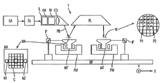
− この特別なケースでは放射線ソースLAも備えた、放射線の投影ビームPBを供給する放射線ソースEx、ILと、
− マスクMA(例えばレクチル)を保持するマスクホルダを備え、かつ、品目PLに対して正確にマスクの位置決めを行う第一位置決め手段に連結を行った第一オブジェクトテーブル(マスクテーブル)MTと、
− 基板W(例えばレジスト塗布したシリコンウェハ)を保持する基板ホルダを備え、かつ、品目PLに対して正確に基板の位置決めを行う第二位置決め手段に連結を行った第二オブジェクトテーブル(基板テーブル)WTと、
− マスクMAの照射部分を、基板Wの目標部分C(例えば、1つあるいはそれ以上のダイから成る)に描像する投影システム(「レンズ」)PL(例えば屈折性、反射性または反射屈折性光学システム)とにより構成されている。
1.ステップモードにおいては、マスクテーブルMTは基本的に静止状態に保たれている。そして、マスクの像全体が1回の作動(すなわち1回の「フラッシュ」)で目標部分Cに投影される。次に基板テーブルWTがx方向および/あるいはy方向にシフトされ、異なる目標部分CがビームPBにより照射され得る。
2.走査モードにおいては、基本的に同一シナリオが適用されるが、但し、ここでは、所定の目標部分Cは1回の「フラッシュ」では露光されない。代わって、マスクテーブルMTが、速度vにて所定方向(いわゆる「走査方向」、例えばy方向)に運動可能であり、それによってビームPBがマスクの像を走査する。これと同時に、基板テーブルWTが速度V=Mvで、同一方向あるいは反対方向に運動する。ここで、MはレンズPLの倍率(一般的にM=1/4あるいは1/5)である。このように、解像度を妥協することなく、比較的大きな目標部分Cを露光することが可能となる。
Claims (10)
- 光学システムを使用してマスクに対して基板の表面に形成すべきパターンの強度プロフィールを最適化する方法であって、
前記マスクの印刷挙動を表す数学的関数を生成するステップと、
前記光学システムの特徴を表す固有関数を生成するステップと、
前記固有関数をフィルタリングするステップと、
前記フィルタリングした固有関数を前記数学的関数で畳み込んで干渉マップを生成するステップと、
前記干渉マップに基づいて前記マスクの補助フューチャを決定するステップと、
を備える方法。 - 前記固有関数をフィルタリングするステップは、前記固有関数の副ローブをフィルタリングするステップを含む、請求項1に記載の方法。
- 前記固有関数をフィルタリングするステップは、前記固有関数の主ローブの外側をフィルタリングするステップを含む、請求項1に記載の方法。
- 前記固有関数をフィルタリングするステップは、前記固有関数のDC成分又は特定の低い空間周波数を除去するステップを含む、請求項1に記載の方法。
- 前記固有関数をフィルタリングするステップは、同相補助フューチャと位相ずれ補助フューチャの局所的不均衡を最小にするステップを含む、請求項1乃至請求項4のうち何れか1項に記載の方法。
- 少なくとも1つのマシンで読み出し可能な媒体によって転送可能な実行可能コードを有するプログラムであって、プログラマブルコンピュータによって前記実行可能コードを実行すると、前記プログラマブルコンピュータが、光学システムを使用してマスクに対して基板の表面に形成すべきパターンの強度プロフィールを最適化するために、
前記マスクの印刷挙動を表す数学的関数を生成するステップと、
前記光学システムの特徴を表す固有関数を生成するステップと、
前記固有関数をフィルタリングするステップと、
前記フィルタリングした固有関数を前記数学的関数で畳み込んで干渉マップを生成するステップと、
前記干渉マップに基づいて前記マスクの補助フューチャを決定するステップと、
を実行するプログラム。 - 前記固有関数をフィルタリングするステップは、前記固有関数の副ローブをフィルタリングするステップを含む、請求項6に記載のプログラム。
- 前記固有関数をフィルタリングするステップは、前記固有関数の主ローブの外側をフィルタリングするステップを含む、請求項6に記載のプログラム。
- 前記固有関数をフィルタリングするステップは、前記固有関数のDC成分又は特定の低い空間周波数を除去するステップを含む、請求項6に記載のプログラム。
- 前記固有関数をフィルタリングするステップは、同相補助フューチャと位相ずれ補助フューチャの局所的不均衡を最小にするステップを含む、請求項6乃至請求項9のうち何れか1項に記載のプログラム。
Applications Claiming Priority (2)
| Application Number | Priority Date | Filing Date | Title |
|---|---|---|---|
| US51570803P | 2003-10-31 | 2003-10-31 | |
| US515708 | 2003-10-31 |
Publications (2)
| Publication Number | Publication Date |
|---|---|
| JP2005141241A JP2005141241A (ja) | 2005-06-02 |
| JP5121117B2 true JP5121117B2 (ja) | 2013-01-16 |
Family
ID=34421829
Family Applications (1)
| Application Number | Title | Priority Date | Filing Date |
|---|---|---|---|
| JP2004344913A Expired - Fee Related JP5121117B2 (ja) | 2003-10-31 | 2004-10-29 | 強度プロフィールを最適化する方法及びプログラム |
Country Status (7)
| Country | Link |
|---|---|
| US (1) | US7231629B2 (ja) |
| EP (1) | EP1528429A3 (ja) |
| JP (1) | JP5121117B2 (ja) |
| KR (1) | KR100927454B1 (ja) |
| CN (1) | CN100576066C (ja) |
| SG (1) | SG111285A1 (ja) |
| TW (1) | TWI377438B (ja) |
Families Citing this family (30)
| Publication number | Priority date | Publication date | Assignee | Title |
|---|---|---|---|---|
| TW200523524A (en) * | 2003-11-05 | 2005-07-16 | Asml Masktools Bv | Eigen decomposition based OPC model |
| US7057709B2 (en) * | 2003-12-04 | 2006-06-06 | International Business Machines Corporation | Printing a mask with maximum possible process window through adjustment of the source distribution |
| US7506299B2 (en) * | 2003-12-19 | 2009-03-17 | Asml Holding N.V. | Feature optimization using interference mapping lithography |
| US7310796B2 (en) * | 2004-08-27 | 2007-12-18 | Applied Materials, Israel, Ltd. | System and method for simulating an aerial image |
| US7331033B2 (en) * | 2004-08-27 | 2008-02-12 | Applied Materials, Israel, Ltd. | Simulation of aerial images |
| US7509621B2 (en) * | 2005-01-03 | 2009-03-24 | Synopsys, Inc. | Method and apparatus for placing assist features by identifying locations of constructive and destructive interference |
| US7200835B2 (en) * | 2005-02-24 | 2007-04-03 | Texas Instruments Incorporated | Method of locating sub-resolution assist feature(s) |
| US8037429B2 (en) * | 2005-03-02 | 2011-10-11 | Mentor Graphics Corporation | Model-based SRAF insertion |
| JP4790350B2 (ja) * | 2005-08-31 | 2011-10-12 | 富士通セミコンダクター株式会社 | 露光用マスク及び露光用マスクの製造方法 |
| US7614034B2 (en) * | 2005-11-08 | 2009-11-03 | Asml Masktools B.V. | Method and apparatus for generating OPC rules for placement of scattering bar features utilizing interface mapping technology |
| JP2008076683A (ja) * | 2006-09-20 | 2008-04-03 | Canon Inc | 原版データ作成プログラム、原版データ作成方法、原版作成方法、露光方法及びデバイスの製造方法 |
| JP4804294B2 (ja) * | 2006-09-20 | 2011-11-02 | キヤノン株式会社 | 原版データ作成プログラム、原版データ作成方法、原版作成方法、露光方法及びデバイスの製造方法 |
| US8341561B2 (en) | 2006-12-12 | 2012-12-25 | Samsung Electronics Co., Ltd. | Methods of arranging mask patterns and associated apparatus |
| KR100874913B1 (ko) | 2006-12-12 | 2008-12-19 | 삼성전자주식회사 | 마스크 패턴을 배치하는 방법 및 이를 이용한 장치 |
| KR100881184B1 (ko) | 2006-12-12 | 2009-02-05 | 삼성전자주식회사 | 마스크 패턴을 배치하는 방법 및 이를 이용한 장치 |
| US7799487B2 (en) * | 2007-02-09 | 2010-09-21 | Ayman Yehia Hamouda | Dual metric OPC |
| US7882480B2 (en) * | 2007-06-04 | 2011-02-01 | Asml Netherlands B.V. | System and method for model-based sub-resolution assist feature generation |
| JP5479328B2 (ja) * | 2007-06-04 | 2014-04-23 | エーエスエムエル ネザーランズ ビー.ブイ. | モデルベースのリソグラフィ誘導レイアウト設計を実行するための方法 |
| JP4484909B2 (ja) * | 2007-07-24 | 2010-06-16 | キヤノン株式会社 | 原版データ作成方法、原版作成方法、露光方法および原版データ作成プログラム |
| US9779186B2 (en) | 2007-08-28 | 2017-10-03 | Asml Netherlands B.V. | Methods for performing model-based lithography guided layout design |
| US7930657B2 (en) * | 2008-01-23 | 2011-04-19 | Micron Technology, Inc. | Methods of forming photomasks |
| US7954071B2 (en) * | 2008-10-31 | 2011-05-31 | Synopsys, Inc. | Assist feature placement based on a focus-sensitive cost-covariance field |
| JP5185235B2 (ja) * | 2009-09-18 | 2013-04-17 | 株式会社東芝 | フォトマスクの設計方法およびフォトマスクの設計プログラム |
| DE102010004939A1 (de) * | 2010-01-18 | 2011-07-21 | EQUIcon Software GmbH Jena, 07745 | Verfahren zur Steuerung der Elektronenstrahl-Belichtung von Wafern und Masken mit Proximity-Korrektur |
| US8846273B2 (en) | 2012-06-04 | 2014-09-30 | Micron Technology, Inc. | Photomasks, methods of forming a photomask, and methods of photolithographically patterning a substrate |
| KR101991380B1 (ko) | 2012-07-26 | 2019-06-20 | 삼성전자주식회사 | 반도체 소자의 레이아웃 생성 방법 |
| CN106556974B (zh) * | 2015-09-30 | 2019-04-26 | 中芯国际集成电路制造(上海)有限公司 | 光刻照明系统以及光刻设备 |
| US11301610B2 (en) | 2017-12-22 | 2022-04-12 | D2S, Inc. | Methods for modeling of a design in reticle enhancement technology |
| US10657213B2 (en) | 2017-12-22 | 2020-05-19 | D2S, Inc. | Modeling of a design in reticle enhancement technology |
| CN113378412B (zh) * | 2021-08-12 | 2021-11-02 | 南京科远智慧科技集团股份有限公司 | 一种应用于tdlas线形拟合算法的激光器特性变化修正方法 |
Family Cites Families (25)
| Publication number | Priority date | Publication date | Assignee | Title |
|---|---|---|---|---|
| JPH04216548A (ja) * | 1990-12-18 | 1992-08-06 | Mitsubishi Electric Corp | フォトマスク |
| KR960002536A (ja) * | 1994-06-29 | 1996-01-26 | ||
| US5682323A (en) * | 1995-03-06 | 1997-10-28 | Lsi Logic Corporation | System and method for performing optical proximity correction on macrocell libraries |
| NL1005841C2 (nl) | 1997-04-18 | 1998-10-20 | Dsm Nv | Can- en coilcoatingharsen. |
| JPH1115130A (ja) * | 1997-06-24 | 1999-01-22 | Matsushita Electron Corp | 半導体製造用ハーフトーンマスクおよびその製造方法 |
| US6223139B1 (en) * | 1998-09-15 | 2001-04-24 | International Business Machines Corporation | Kernel-based fast aerial image computation for a large scale design of integrated circuit patterns |
| JP3275863B2 (ja) * | 1999-01-08 | 2002-04-22 | 日本電気株式会社 | フォトマスク |
| US6214497B1 (en) * | 1999-06-29 | 2001-04-10 | Micron Technology, Inc. | Method to eliminate side lobe printing of attenuated phase shift masks |
| US6303253B1 (en) * | 2000-03-16 | 2001-10-16 | International Business Machines Corporation | Hierarchy and domain-balancing method and algorithm for serif mask design in microlithography |
| US6503666B1 (en) | 2000-07-05 | 2003-01-07 | Numerical Technologies, Inc. | Phase shift masking for complex patterns |
| US6777141B2 (en) * | 2000-07-05 | 2004-08-17 | Numerical Technologies, Inc. | Phase shift mask including sub-resolution assist features for isolated spaces |
| US6787271B2 (en) * | 2000-07-05 | 2004-09-07 | Numerical Technologies, Inc. | Design and layout of phase shifting photolithographic masks |
| TW552561B (en) | 2000-09-12 | 2003-09-11 | Asml Masktools Bv | Method and apparatus for fast aerial image simulation |
| US6901575B2 (en) * | 2000-10-25 | 2005-05-31 | Numerical Technologies, Inc. | Resolving phase-shift conflicts in layouts using weighted links between phase shifters |
| TWI285295B (en) * | 2001-02-23 | 2007-08-11 | Asml Netherlands Bv | Illumination optimization in lithography |
| US6519760B2 (en) | 2001-02-28 | 2003-02-11 | Asml Masktools, B.V. | Method and apparatus for minimizing optical proximity effects |
| US6792591B2 (en) * | 2001-02-28 | 2004-09-14 | Asml Masktools B.V. | Method of identifying an extreme interaction pitch region, methods of designing mask patterns and manufacturing masks, device manufacturing methods and computer programs |
| KR100576752B1 (ko) * | 2001-10-09 | 2006-05-03 | 에이에스엠엘 마스크툴즈 비.브이. | 2차원 피처모델 캘리브레이션 및 최적화 방법 |
| JP3592666B2 (ja) * | 2001-12-04 | 2004-11-24 | 株式会社東芝 | 露光用マスクパターンの補正方法、プログラム、マスクパターン形成方法、及び半導体装置の製造方法 |
| US6749970B2 (en) | 2001-12-11 | 2004-06-15 | Advanced Micro Devices, Inc. | Method of enhancing clear field phase shift masks with border regions around phase 0 and phase 180 regions |
| US7023528B2 (en) * | 2002-06-10 | 2006-04-04 | International Business Machines Corporation | Hybrid electronic mask |
| US6807662B2 (en) * | 2002-07-09 | 2004-10-19 | Mentor Graphics Corporation | Performance of integrated circuit components via a multiple exposure technique |
| US7266480B2 (en) * | 2002-10-01 | 2007-09-04 | The Regents Of The University Of California | Rapid scattering simulation of objects in imaging using edge domain decomposition |
| SG125109A1 (en) | 2003-01-14 | 2006-09-29 | Asml Masktools Bv | Method and apparatus for providing optical proximity features to a reticle pattern for deep sub-wavelength optical lithography |
| US7594199B2 (en) * | 2003-01-14 | 2009-09-22 | Asml Masktools B.V. | Method of optical proximity correction design for contact hole mask |
-
2004
- 2004-10-29 KR KR1020040087192A patent/KR100927454B1/ko not_active IP Right Cessation
- 2004-10-29 TW TW093133057A patent/TWI377438B/zh not_active IP Right Cessation
- 2004-10-29 US US10/976,306 patent/US7231629B2/en active Active
- 2004-10-29 CN CN200410103875A patent/CN100576066C/zh not_active Expired - Fee Related
- 2004-10-29 JP JP2004344913A patent/JP5121117B2/ja not_active Expired - Fee Related
- 2004-10-29 EP EP04256714A patent/EP1528429A3/en not_active Withdrawn
- 2004-11-01 SG SG200406371A patent/SG111285A1/en unknown
Also Published As
| Publication number | Publication date |
|---|---|
| US20050149900A1 (en) | 2005-07-07 |
| CN1629735A (zh) | 2005-06-22 |
| CN100576066C (zh) | 2009-12-30 |
| EP1528429A2 (en) | 2005-05-04 |
| JP2005141241A (ja) | 2005-06-02 |
| KR100927454B1 (ko) | 2009-11-19 |
| EP1528429A3 (en) | 2006-04-12 |
| TWI377438B (en) | 2012-11-21 |
| US7231629B2 (en) | 2007-06-12 |
| TW200527152A (en) | 2005-08-16 |
| SG111285A1 (en) | 2005-05-30 |
| KR20050041958A (ko) | 2005-05-04 |
Similar Documents
| Publication | Publication Date | Title |
|---|---|---|
| JP5121117B2 (ja) | 強度プロフィールを最適化する方法及びプログラム | |
| JP3992688B2 (ja) | コンタクト・ホール・マスクの光学的近接補正設計の方法 | |
| JP4101770B2 (ja) | ディープ・サブ波長の光リソグラフィのためのレチクル・パターンに光近接フィーチャを提供する方法および装置 | |
| US10657641B2 (en) | Source and mask optimization by changing intensity and shape of the illumination source and magnitude and phase of mask diffraction orders | |
| JP4383400B2 (ja) | 1/4波長リソグラフィの焦点深さを上げるためにモデルに基づき散乱バーを配置する方法、プログラム製品および装置 | |
| US7506299B2 (en) | Feature optimization using interference mapping lithography | |
| JP4267245B2 (ja) | 解像度以下の補助フィーチャとして罫線ラダー・バーを利用した光近接補正方法 | |
| KR100865768B1 (ko) | 다크 필드 더블 이중극 리소그래피(ddl)를 수행하는방법 및 장치 | |
| US7550235B2 (en) | Method and apparatus for performing model based placement of phase-balanced scattering bars for sub-wavelength optical lithography | |
| JP4602962B2 (ja) | 多重露光プロセスに用いられるモデルベースのジオメトリ分解のための方法、プログラム製品及び装置 | |
| KR100927455B1 (ko) | 간섭 매핑 리소그래피를 이용한 피처 최적화 방법 | |
| US20050053848A1 (en) | Method, program product and apparatus for generating assist features utilizing an image field map | |
| KR20030077447A (ko) | 무크롬 상 리소그래피를 이용하여 상 및 크롬영역으로반도체디바이스패턴을 분해하는 방법 및 장치 | |
| KR100563776B1 (ko) | 공간 주파수 2배가 기술을 활용하여 마스크패턴을형성하는 방법 및 장치 | |
| US7604909B2 (en) | Method for improved manufacturability and patterning of sub-wavelength contact hole mask |
Legal Events
| Date | Code | Title | Description |
|---|---|---|---|
| RD03 | Notification of appointment of power of attorney |
Free format text: JAPANESE INTERMEDIATE CODE: A7423 Effective date: 20060904 |
|
| A621 | Written request for application examination |
Free format text: JAPANESE INTERMEDIATE CODE: A621 Effective date: 20070329 |
|
| RD05 | Notification of revocation of power of attorney |
Free format text: JAPANESE INTERMEDIATE CODE: A7425 Effective date: 20070517 |
|
| A977 | Report on retrieval |
Free format text: JAPANESE INTERMEDIATE CODE: A971007 Effective date: 20091214 |
|
| A131 | Notification of reasons for refusal |
Free format text: JAPANESE INTERMEDIATE CODE: A131 Effective date: 20091216 |
|
| A521 | Written amendment |
Free format text: JAPANESE INTERMEDIATE CODE: A523 Effective date: 20100309 |
|
| A131 | Notification of reasons for refusal |
Free format text: JAPANESE INTERMEDIATE CODE: A131 Effective date: 20110907 |
|
| A521 | Written amendment |
Free format text: JAPANESE INTERMEDIATE CODE: A523 Effective date: 20111115 |
|
| TRDD | Decision of grant or rejection written | ||
| A01 | Written decision to grant a patent or to grant a registration (utility model) |
Free format text: JAPANESE INTERMEDIATE CODE: A01 Effective date: 20121004 |
|
| A01 | Written decision to grant a patent or to grant a registration (utility model) |
Free format text: JAPANESE INTERMEDIATE CODE: A01 |
|
| A61 | First payment of annual fees (during grant procedure) |
Free format text: JAPANESE INTERMEDIATE CODE: A61 Effective date: 20121023 |
|
| FPAY | Renewal fee payment (event date is renewal date of database) |
Free format text: PAYMENT UNTIL: 20151102 Year of fee payment: 3 |
|
| R150 | Certificate of patent or registration of utility model |
Free format text: JAPANESE INTERMEDIATE CODE: R150 |
|
| S111 | Request for change of ownership or part of ownership |
Free format text: JAPANESE INTERMEDIATE CODE: R313113 |
|
| R360 | Written notification for declining of transfer of rights |
Free format text: JAPANESE INTERMEDIATE CODE: R360 |
|
| R360 | Written notification for declining of transfer of rights |
Free format text: JAPANESE INTERMEDIATE CODE: R360 |
|
| R371 | Transfer withdrawn |
Free format text: JAPANESE INTERMEDIATE CODE: R371 |
|
| LAPS | Cancellation because of no payment of annual fees |