EP1540786B1 - Dispositif laser a semi-conducteur - Google Patents
Dispositif laser a semi-conducteur Download PDFInfo
- Publication number
- EP1540786B1 EP1540786B1 EP03790845A EP03790845A EP1540786B1 EP 1540786 B1 EP1540786 B1 EP 1540786B1 EP 03790845 A EP03790845 A EP 03790845A EP 03790845 A EP03790845 A EP 03790845A EP 1540786 B1 EP1540786 B1 EP 1540786B1
- Authority
- EP
- European Patent Office
- Prior art keywords
- semiconductor laser
- laser device
- laser element
- reflection means
- individual
- Prior art date
- Legal status (The legal status is an assumption and is not a legal conclusion. Google has not performed a legal analysis and makes no representation as to the accuracy of the status listed.)
- Expired - Lifetime
Links
- 239000004065 semiconductor Substances 0.000 title claims abstract description 108
- 238000001228 spectrum Methods 0.000 claims abstract description 7
- 230000009466 transformation Effects 0.000 claims description 15
- 238000003491 array Methods 0.000 description 2
- BJQHLKABXJIVAM-UHFFFAOYSA-N bis(2-ethylhexyl) phthalate Chemical compound CCCCC(CC)COC(=O)C1=CC=CC=C1C(=O)OCC(CC)CCCC BJQHLKABXJIVAM-UHFFFAOYSA-N 0.000 description 2
- 230000008878 coupling Effects 0.000 description 2
- 238000010168 coupling process Methods 0.000 description 2
- 238000005859 coupling reaction Methods 0.000 description 2
- 230000003287 optical effect Effects 0.000 description 2
- 230000005855 radiation Effects 0.000 description 2
- 230000003321 amplification Effects 0.000 description 1
- 239000006117 anti-reflective coating Substances 0.000 description 1
- 230000015572 biosynthetic process Effects 0.000 description 1
- 239000011248 coating agent Substances 0.000 description 1
- 238000000576 coating method Methods 0.000 description 1
- 239000013078 crystal Substances 0.000 description 1
- 238000005516 engineering process Methods 0.000 description 1
- 239000003365 glass fiber Substances 0.000 description 1
- 238000004519 manufacturing process Methods 0.000 description 1
- 238000000034 method Methods 0.000 description 1
- 238000003199 nucleic acid amplification method Methods 0.000 description 1
- 238000005215 recombination Methods 0.000 description 1
- 230000006798 recombination Effects 0.000 description 1
- 230000003595 spectral effect Effects 0.000 description 1
Images
Classifications
-
- H—ELECTRICITY
- H01—ELECTRIC ELEMENTS
- H01S—DEVICES USING THE PROCESS OF LIGHT AMPLIFICATION BY STIMULATED EMISSION OF RADIATION [LASER] TO AMPLIFY OR GENERATE LIGHT; DEVICES USING STIMULATED EMISSION OF ELECTROMAGNETIC RADIATION IN WAVE RANGES OTHER THAN OPTICAL
- H01S5/00—Semiconductor lasers
- H01S5/40—Arrangement of two or more semiconductor lasers, not provided for in groups H01S5/02 - H01S5/30
- H01S5/4025—Array arrangements, e.g. constituted by discrete laser diodes or laser bar
- H01S5/4031—Edge-emitting structures
- H01S5/4062—Edge-emitting structures with an external cavity or using internal filters, e.g. Talbot filters
-
- H—ELECTRICITY
- H01—ELECTRIC ELEMENTS
- H01S—DEVICES USING THE PROCESS OF LIGHT AMPLIFICATION BY STIMULATED EMISSION OF RADIATION [LASER] TO AMPLIFY OR GENERATE LIGHT; DEVICES USING STIMULATED EMISSION OF ELECTROMAGNETIC RADIATION IN WAVE RANGES OTHER THAN OPTICAL
- H01S5/00—Semiconductor lasers
- H01S5/10—Construction or shape of the optical resonator, e.g. extended or external cavity, coupled cavities, bent-guide, varying width, thickness or composition of the active region
- H01S5/14—External cavity lasers
-
- H—ELECTRICITY
- H01—ELECTRIC ELEMENTS
- H01S—DEVICES USING THE PROCESS OF LIGHT AMPLIFICATION BY STIMULATED EMISSION OF RADIATION [LASER] TO AMPLIFY OR GENERATE LIGHT; DEVICES USING STIMULATED EMISSION OF ELECTROMAGNETIC RADIATION IN WAVE RANGES OTHER THAN OPTICAL
- H01S5/00—Semiconductor lasers
- H01S5/06—Arrangements for controlling the laser output parameters, e.g. by operating on the active medium
- H01S5/065—Mode locking; Mode suppression; Mode selection ; Self pulsating
-
- H—ELECTRICITY
- H01—ELECTRIC ELEMENTS
- H01S—DEVICES USING THE PROCESS OF LIGHT AMPLIFICATION BY STIMULATED EMISSION OF RADIATION [LASER] TO AMPLIFY OR GENERATE LIGHT; DEVICES USING STIMULATED EMISSION OF ELECTROMAGNETIC RADIATION IN WAVE RANGES OTHER THAN OPTICAL
- H01S5/00—Semiconductor lasers
- H01S5/02—Structural details or components not essential to laser action
- H01S5/026—Monolithically integrated components, e.g. waveguides, monitoring photo-detectors, drivers
- H01S5/0267—Integrated focusing lens
-
- H—ELECTRICITY
- H01—ELECTRIC ELEMENTS
- H01S—DEVICES USING THE PROCESS OF LIGHT AMPLIFICATION BY STIMULATED EMISSION OF RADIATION [LASER] TO AMPLIFY OR GENERATE LIGHT; DEVICES USING STIMULATED EMISSION OF ELECTROMAGNETIC RADIATION IN WAVE RANGES OTHER THAN OPTICAL
- H01S5/00—Semiconductor lasers
- H01S5/06—Arrangements for controlling the laser output parameters, e.g. by operating on the active medium
- H01S5/065—Mode locking; Mode suppression; Mode selection ; Self pulsating
- H01S5/0656—Seeding, i.e. an additional light input is provided for controlling the laser modes, for example by back-reflecting light from an external optical component
-
- H—ELECTRICITY
- H01—ELECTRIC ELEMENTS
- H01S—DEVICES USING THE PROCESS OF LIGHT AMPLIFICATION BY STIMULATED EMISSION OF RADIATION [LASER] TO AMPLIFY OR GENERATE LIGHT; DEVICES USING STIMULATED EMISSION OF ELECTROMAGNETIC RADIATION IN WAVE RANGES OTHER THAN OPTICAL
- H01S5/00—Semiconductor lasers
- H01S5/40—Arrangement of two or more semiconductor lasers, not provided for in groups H01S5/02 - H01S5/30
- H01S5/4012—Beam combining, e.g. by the use of fibres, gratings, polarisers, prisms
-
- H—ELECTRICITY
- H01—ELECTRIC ELEMENTS
- H01S—DEVICES USING THE PROCESS OF LIGHT AMPLIFICATION BY STIMULATED EMISSION OF RADIATION [LASER] TO AMPLIFY OR GENERATE LIGHT; DEVICES USING STIMULATED EMISSION OF ELECTROMAGNETIC RADIATION IN WAVE RANGES OTHER THAN OPTICAL
- H01S5/00—Semiconductor lasers
- H01S5/40—Arrangement of two or more semiconductor lasers, not provided for in groups H01S5/02 - H01S5/30
- H01S5/4025—Array arrangements, e.g. constituted by discrete laser diodes or laser bar
- H01S5/4031—Edge-emitting structures
Definitions
- the present invention relates to a semiconductor laser device according to the preamble of claim 1.
- a semiconductor laser device of the aforementioned type is known from US-A-4,656,641.
- the semiconductor laser device described therein comprises a semiconductor laser element having a plurality of exit surfaces for the laser radiation.
- the semiconductor laser device further includes an external resonator including a concave mirror spaced from the semiconductor laser element and capable of reflecting the laser light back into the semiconductor laser element.
- Another semiconductor laser device is known in US Pat. No. 6,404,797.
- the device described therein is embodied as an array of VCSEL laser diodes, in which the laser radiation exits the laser diodes perpendicular to the active layer.
- Each laser diode of this array is in each case associated with an external reflector designed, for example, as a concave mirror, which is part of an external resonator of the semiconductor laser device.
- Another semiconductor laser device is known from I. Nelson, B. Chann, TG Walker, Opt. Lett. 25, 1352 (2000).
- an external resonator is used which uses a grating as a reflection means.
- a fast-axis collimating lens is used in the external resonator directly following the semiconductor laser element.
- two telescoping lenses are arranged in the external resonator.
- a disadvantage of such a semiconductor laser device proves that on the one hand due to the many optical components within the external resonator comparatively high losses occur, so that the output power of the semiconductor laser device is comparatively low.
- the semiconductor laser device known from the prior art only the longitudinal modes of the semiconductor laser element or of the individual emitters of the semiconductor laser element can be influenced.
- the design known from the prior art can not influence the transverse mode spectrum of the semiconductor laser device. For this reason, this prior art semiconductor laser device will have a plurality of different transverse modes per emitter, all of which contribute to the laser light emitted from the semiconductor laser device. Due to this fact, the laser light emerging from the semiconductor laser device according to this prior art is difficult to focus.
- the mode spectrum of semiconductor laser elements is further attempted to influence the mode spectrum of semiconductor laser elements by structuring the active zone of the semiconductor laser element.
- These structurings may, for example, comprise changes of the refractive index in different directions, so that the propagation of individual preferred transverse laser modes is preferred by these refractive indices varying in different directions.
- Both aforementioned methods for the preference of individual transverse modes are associated with considerable manufacturing effort and also do not give any truly satisfactory beam quality or output power of the semiconductor laser device.
- the problem underlying the present invention is the provision of a semiconductor laser device of the type mentioned, which has a high output power with improved beam quality.
- the reflecting surfaces can reflect back the corresponding partial beams of the laser light onto the respective exit surfaces such that they serve as an aperture.
- the semiconductor laser device may include a lens means disposed between the reflecting means and the semiconductor laser element or the individual emitters, which may at least partially reduce the divergence of the laser light at least in the first direction.
- This lens means thus serves as a fast-axis collimating lens.
- the semiconductor laser device comprises a Beam transformation unit, which is designed in particular as a jet rotation unit and can preferably each rotate individual sub-beams, in particular by about 90 °.
- a Beam transformation unit designed in particular as a jet rotation unit and can preferably each rotate individual sub-beams, in particular by about 90 °.
- the beam transformation unit is arranged between the reflection means and the semiconductor laser element or the individual lasers, in particular between the reflection means and the lens means.
- Such an arrangement of the beam transformation unit within the external resonator can provide more space for decoupling.
- the semiconductor laser device may further comprise a frequency doubling element disposed between the reflection means and the semiconductor laser element or the single lasers, in particular between the reflection means and the lens means.
- the second harmonic could be at least partially decoupled from the semiconductor laser device and the fundamental wavelength for influencing the mode spectrum at least partially reflected back into the semiconductor laser element or the individual laser.
- the semiconductor laser element it is also possible for the semiconductor laser element to be supplied with voltage or supplied with current for generating electron-hole pairs only in partial regions which correspond to the spatial extent of a desired mode of the laser light.
- the preference for desired modes of the laser light can be further optimized.
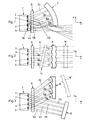
- the example of a semiconductor laser device shown in FIG. 1 comprises a semiconductor laser element 1 having a plurality of exit surfaces 2, 3, 4, 5, from which laser light can emerge.
- the semiconductor laser element 1 is designed as a broad-band emitter array or as a so-called laser diode bar. In the illustrated embodiment, only four of the light emissions serving separated exit surfaces 2, 3, 4, 5 are located. However, there is the possibility that a substantial larger number of parallel and spaced spaced exit surfaces is provided.
- the laser light emerging from each of the exit surfaces 2, 3, 4, 5 is in each case divided into two partial beams 2a, 2b; 3a, 3b; 4a, 4b; 5a, 5b split, which in each case with the normal on the exit surfaces 2, 3, 4, 5 include an opposite equal angle.
- the two respectively associated partial beams 2a, 2b; 3a, 3b; 4a, 4b; 5a, 5b each represent an extracted laser mode of the emitting area of the semiconductor laser element 1 belonging to the corresponding exit area 2, 3, 4, 5.
- a semiconductor laser device further comprises, outside the semiconductor laser element 1, a lens means 6 which is designed as a fast axis collimating lens.
- the fast axis corresponds in the drawn Cartesian coordinate system of the Y direction.
- the fast axis is in such wide-strip emitters the direction perpendicular to the direction in which the individual emitters are arranged side by side.
- the divergence of such a semiconductor laser element 1 in the fast axis is substantially greater than in the vertical axis perpendicular thereto, which corresponds to the X direction in FIG.
- a reflection means 7 having a reflective surface 8 facing the semiconductor laser element 1 is arranged at a suitable distance from the semiconductor laser element 1.
- the partial beams 2a, 3a, 4a, 5a are reflected back in the direction of the exit surfaces 2, 3, 4, 5.
- the exit surfaces 2, 3, 4, 5 are provided with an anti-reflective coating, so that the back-reflected partial beams 2a, 3a, 4a, 5a can at least partially penetrate into the semiconductor laser element 1 such that the mode spectrum of the semiconductor laser element 1 being affected.
- focal length and distance of the reflection means 7 with respect to the exit surfaces 2, 3, 4, 5, the propagation of certain modes in the semiconductor laser element 1 may be preferred.
- not all laser emitters which are assigned to the individual exit surfaces 2, 3, 4, 5 are usually oscillated in the same mode, because the angles at which the partial beams 2a, 3a, 4a, 5a exit from the exit surfaces 2, 3, 4, 5, are slightly different.
- the distance of the reflective surface 8 from the exit surfaces 2, 3, 4, 5 can be chosen so that it substantially corresponds to the focal length of the reflective surface 8.
- by appropriate choice of the distance or the focal length of the beam waist on the exit surfaces 2, 3, 4, 5 correspond approximately to their respective width.
- the coupling out of the semiconductor laser device according to FIG. 1 can take place via the partial beams 2b, 3b, 4b, 5b.
- a further partially reflecting reflection means may be inserted, which serves as an output coupler.
- FIG. 2 In the embodiment of a semiconductor laser device according to the invention shown in FIG. 2, like parts are given the same reference numerals.
- Fig. 2 partial beams 2c, 3c, 4c, 5c are shown, which correspond to a transverse mode of the individual emitter of the semiconductor laser element 1, which in essentially parallel to the normal on the exit surfaces 2, 3, 4, 5, ie approximately in the Z direction according to the Cartesian coordinate system, emerges from the semiconductor laser element 1.
- the reflection means 9 provided in FIG. 2 has not only a reflective surface but a plurality of reflective surfaces 10, 11, 12, 13.
- each of the sub-beams 2c, 3c, 4c, 5c is associated with one of the reflective surfaces 10, 11, 12, 13, so that in this embodiment, each of the emitter of the semiconductor laser element 1 corresponding to the exit surfaces 2, 3, 4, 5 is in the same transverse or longitudinal mode can be operated.
- a wave-selective element 14 is shown in dashed lines in FIG. 2, which can be embodied, for example, as an etalon.
- the optional wave-selective element 14 makes it possible to select certain longitudinal modes, in particular a longitudinal mode, so that the emitted laser light has a small spectral width.
- the coupling out of the semiconductor laser device can be achieved either by designing the reflection means 9 to be partially reflecting, so that laser light can emerge from the reflection means 9 in the positive Z direction.
- the side of the semiconductor laser element facing away from the external resonator formed by the reflection means 9 may be partially anti-reflection or not highly reflective, so that laser light may leak in the negative Z direction on the left side in FIG. 2 of the semiconductor laser element ,
- the Reflecting means 9 is arranged similar reflection means, which can reflect back from the semiconductor laser element 1 in the negative Z-direction emerging laser light in the semiconductor laser element 1.
- the external resonator is formed in this case by the two reflection means 9, whose reflective surfaces face each other.
- One of the reflection means 9 may be formed partially reflecting, so that the laser light can partially pass through this reflection means for decoupling.
- a beam transformation unit 15 is further shown in dashed lines on the right side of the reflection means, which can transform the light beam in the positive Z direction from the reflection means 9, the beam.
- the beam transformation unit can be a beam rotation unit which can individually rotate each of the partial beams 2c, 3c, 4c, 5c by 90 °, for example. By such a beam transformation, the focusability of the exiting laser light is improved. It is quite possible according to the invention to use such a beam transformation unit also in the embodiment according to FIG.
- the semiconductor laser device according to FIG. 3 essentially differs from that in FIG. 2 in that modes are preferred which, according to FIG. 1, emerge from the exit surfaces 2, 3, 4, 5 at an angle to the normal.
- the reflection means 16 provided in the semiconductor laser device according to FIG. 3 again has a multiplicity of reflective surfaces 17, 18, 19, 20. In the solid-drawn embodiment of the reflection means 16 this is oriented substantially parallel to the X direction, so that the paths of the individual partial beams 2a, 3a, 4a, 5a between the exit surfaces 2, 3, 4, 5 and the reflective surfaces 17, 18, 19, 20 are the same.
- a reflection means 16 ' may be provided, which is shown in phantom in Fig. 3 and may be incorporated in the same place in the semiconductor laser device, as the reflection means 16.
- the individual reflective surfaces 17, 18, 19, 20 are inclined relative to the Z-axis. This is omitted in the reflection means 16 '. However, it may be necessary in this case to make the radii of curvature of the reflective surfaces each different.
- FIG. 3 likewise shows a beam transformation unit 15 which is arranged in the beams 2b, 3b, 4b, 5b to be coupled out.
- the laser light passing through this beam transformation unit 15 can be focused onto the end of a glass fiber, for example, by further focusing means.
- a beam transformation unit designed, for example, as a beam rotation unit rotates the emission of the individual emitters by 90 °. After such a rotation, the partial beams 2a, 3a, 4a, 5a run at equal angles to the X-Z plane up and the partial beams 2b, 3b, 4b, 5b at opposite equal angles down.
- a single cylinder mirror is suitable. If spherical mirrors are to be used, then in the case of slow-axis collimation, a mirror array is needed in this case.
- a stack of emitter arrays is used, a one-shot array of cylinder mirrors could be used for slow-axis collimation in a beam turn unit design.
- a frequency-doubling element for example a frequency-doubling crystal
- this element could be accommodated between the lens means 6 and the reflection means 9 in FIG.
- the reflective surfaces 10, 11, 12, 13 may be highly reflective for the fundamental wavelength and transmissive for the second harmonic wavelength.
- the lens means 6 could be designed in such a way that the fundamental wavelength is transmitted unhindered and the second harmonic is reflected, so that the second harmonic is not fed back into the semiconductor laser element 1.
- a stack of emitter arrays as semiconductor laser element 1.
- a two-dimensional array of spherical or cylindrical mirrors or a one-dimensional array of cylindrical mirrors may be used.
- the distance and the focal length can be determined according to the comments on FIG. 1.
- a plurality of separate parallel-mounted single lasers instead of a semiconductor laser element 1 designed as a laser diode bar. These could be operated as a single-mode laser and be controlled individually. Such a plurality of individual lasers is particularly suitable for applications in medical technology.
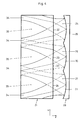
- a semiconductor laser element 21 can be seen that is designed as a laser diode bar.
- the semiconductor laser element 21 has a plurality of exit surfaces 22, 23, 24, from which laser light 25, 26, 27 can emerge.
- a reflection means 28 is provided which has a plurality of juxtaposed reflecting surfaces 29, 30, 31, which are formed, for example, like the reflecting surface 10, 11, 12, 13 according to FIG.
- the corresponding portion of the laser light 25, 26, 27 is also reflected back into the semiconductor laser element 21 by the corresponding exit surfaces 22, 23, 24 of the reflective surfaces 29, 30, 31.
- exit surfaces such as, for example, the middle exit surface 23 in FIG. 4, are provided with a highly reflective coating 33 so that no light can escape from the exit surface 23 from the semiconductor laser element. The light is reflected in this case at this exit surface and exits after further reflection at the opposite end face 32 through one of the adjacent exit surfaces 22, 24 from the semiconductor laser element 21.
- partial regions 34 of the semiconductor laser element 21 are provided with electrodes, so that only these partial regions 34 are supplied with voltage and thus current is supplied only in these partial regions 34 for generating electron holes pairs.
- partial regions 35 are also shown, which are not provided with electrodes and accordingly can not be supplied with voltage.
- a lens means not shown in FIG. 4, between reflection means 28 and semiconductor laser element 21.
Landscapes
- Physics & Mathematics (AREA)
- Condensed Matter Physics & Semiconductors (AREA)
- General Physics & Mathematics (AREA)
- Electromagnetism (AREA)
- Optics & Photonics (AREA)
- Semiconductor Lasers (AREA)
Abstract
Claims (7)
- Dispositif laser à semi-conducteur qui comprend :- un élément laser (1, 21) à semi-conducteur ou plusieurs lasers individuels montés en parallèle et qui présentent plusieurs surfaces de sortie (2, 3, 4, 5, 22, 23, 24) desquelles de la lumière laser sort lorsque le dispositif est en fonctionnement et qui présentent une plus grande divergence dans une première direction (Y) que dans une deuxième direction perpendiculaire à la première, ainsi que- au moins un moyen réfléchissant (7, 9, 16, 16', 28) qui présente au moins une surface réfléchissante à courbure concave (8, 10, 11, 12, 13, 17, 18, 19, 20, 29, 30, 31) et disposé à distance des surfaces de sortie (2, 3, 4, 5, 22, 23, 24) à l'extérieur de l'élément laser (1) à semi-conducteur ou des lasers individuels, et lorsque le dispositif est en fonctionnement, ses surfaces réfléchissantes réfléchissent dans l'élément laser (1, 21) à semi-conducteur ou dans les lasers individuels au moins une partie de la lumière laser sortie de l'élément laser (1, 21) à semi-conducteur ou des lasers individuels par les surfaces de sortie (2, 3, 4, 5, 22, 23, 24), de telle sorte que le spectre de mode de l'élément laser (1, 21) à semi-conducteur ou des lasers individuels soit influencé,caractérisé en ce que- les moyens réfléchissants (9, 16, 16', 28) présentent plusieurs surfaces réfléchissantes individuelles (10, 11, 12, 13, 17, 18, 19, 20, 29, 30, 31) qui réfléchissent chacune l'un des rayons partiels (2a, 2c; 3a, 3c; 4a, 4c; 5a, 5c) qui sortent par les surfaces de sortie individuelles (2, 3, 4, 5, 22, 23, 24).
- Dispositif laser à semi-conducteur selon la revendication 1, caractérisé en ce que les surfaces réfléchissantes (8, 10, 11, 12, 13, 17, 18, 19, 20, 29, 30, 31) peuvent réfléchir une partie des rayons de lumière laser sur les surfaces de sortie (2, 3, 4, 5, 22, 23, 24) pour que celles-ci servent d'ouverture.
- Dispositif laser à semi-conducteur selon l'une des revendications 1 ou 2, caractérisé en ce que le dispositif laser à semi-conducteur comprend un moyen à lentille (6) disposé entre les moyens réfléchissants (7, 9, 16, 16', 28) et l'élément laser (1, 21) à semi-conducteur ou les lasers individuels et qui peut diminuer au moins en partie la divergence de la lumière laser au moins dans la première direction (Y).
- Dispositif laser à semi-conducteur selon l'une des revendications 1 à 3, caractérisé en ce que le dispositif laser à semi-conducteur comprend une unité (15) de transformation des faisceaux qui est réalisée en particulier sous la forme d'unité de rotation des faisceaux et qui peut tourner de préférence chacun des rayons partiels (2a, 2b, 2c; 3a, 3b, 3c; 4a, 4b, 4c; 5a, 5b, 5c) en particulier d'environ 90°.
- Dispositif laser à semi-conducteur selon la revendication 4, caractérisé en ce que l'unité (15) de transformation des faisceaux est disposée entre les moyens réfléchissants (7, 9, 16, 16', 28) et l'élément laser (1) à semi-conducteur ou les lasers individuels, en particulier entre les moyens réfléchissants (7, 9, 16, 16') et le moyen à lentille (6).
- Dispositif laser à semi-conducteur selon l'une des revendications 1 à 5, caractérisé en ce que le dispositif laser à semi-conducteur comprend en outre un élément de doublement de la fréquence qui est disposé entre les moyens réfléchissants (7, 9, 16, 16', 28) et l'élément laser (1, 21)) à semi-conducteur ou les lasers individuels et en particulier entre les moyens réfléchissants (7, 9, 16, 16', 28) et le moyen à lentille (6).
- Dispositif laser à semi-conducteur selon l'une des revendications 1 à 6, caractérisé en ce que l'élément laser (21) à semi-conducteur est sollicité par une tension ou alimenté en courant pour créer des paires électron-trou uniquement dans les parties (34) qui correspondent à l'extension spatiale d'un mode souhaité de la lumière laser.
Applications Claiming Priority (7)
| Application Number | Priority Date | Filing Date | Title |
|---|---|---|---|
| DE10240949 | 2002-09-02 | ||
| DE2002140949 DE10240949A1 (de) | 2002-09-02 | 2002-09-02 | Halbleiterlaservorrichtung |
| DE10250046 | 2002-10-25 | ||
| DE10250048 | 2002-10-25 | ||
| DE10250046 | 2002-10-25 | ||
| DE10250048 | 2002-10-25 | ||
| PCT/EP2003/008526 WO2004021525A2 (fr) | 2002-09-02 | 2003-08-01 | Dispositif laser a semi-conducteur |
Publications (2)
| Publication Number | Publication Date |
|---|---|
| EP1540786A2 EP1540786A2 (fr) | 2005-06-15 |
| EP1540786B1 true EP1540786B1 (fr) | 2007-01-10 |
Family
ID=31981884
Family Applications (1)
| Application Number | Title | Priority Date | Filing Date |
|---|---|---|---|
| EP03790845A Expired - Lifetime EP1540786B1 (fr) | 2002-09-02 | 2003-08-01 | Dispositif laser a semi-conducteur |
Country Status (7)
| Country | Link |
|---|---|
| US (1) | US20060165144A1 (fr) |
| EP (1) | EP1540786B1 (fr) |
| JP (1) | JP2005537643A (fr) |
| KR (1) | KR101033759B1 (fr) |
| AU (1) | AU2003251680A1 (fr) |
| DE (1) | DE50306271D1 (fr) |
| WO (1) | WO2004021525A2 (fr) |
Families Citing this family (17)
| Publication number | Priority date | Publication date | Assignee | Title |
|---|---|---|---|---|
| JP4441918B2 (ja) * | 2006-08-31 | 2010-03-31 | セイコーエプソン株式会社 | 光源装置及び画像表示装置 |
| JP4341685B2 (ja) | 2007-02-22 | 2009-10-07 | セイコーエプソン株式会社 | 光源装置及びプロジェクタ |
| JP4888261B2 (ja) | 2007-07-12 | 2012-02-29 | セイコーエプソン株式会社 | 光源装置、画像表示装置及びモニタ装置 |
| JP4591489B2 (ja) | 2007-08-30 | 2010-12-01 | セイコーエプソン株式会社 | 光源装置、画像表示装置及びモニタ装置 |
| WO2012059864A1 (fr) * | 2010-11-03 | 2012-05-10 | Koninklijke Philips Electronics N.V. | Elément optique pour laser à émission de surface à cavité externe verticale |
| US8891579B1 (en) * | 2011-12-16 | 2014-11-18 | Nlight Photonics Corporation | Laser diode apparatus utilizing reflecting slow axis collimators |
| US9720145B2 (en) | 2014-03-06 | 2017-08-01 | Nlight, Inc. | High brightness multijunction diode stacking |
| US9705289B2 (en) | 2014-03-06 | 2017-07-11 | Nlight, Inc. | High brightness multijunction diode stacking |
| US9525269B2 (en) * | 2014-11-22 | 2016-12-20 | TeraDiode, Inc. | Wavelength beam combining laser systems utilizing etalons |
| US10761276B2 (en) | 2015-05-15 | 2020-09-01 | Nlight, Inc. | Passively aligned crossed-cylinder objective assembly |
| US10261261B2 (en) | 2016-02-16 | 2019-04-16 | Nlight, Inc. | Passively aligned single element telescope for improved package brightness |
| CN109075524B (zh) | 2016-03-18 | 2021-09-03 | 恩耐公司 | 用以提高亮度的光谱复用二极管泵浦模块 |
| CN110199447A (zh) | 2016-12-23 | 2019-09-03 | 恩耐公司 | 低成本光学泵浦激光器封装件 |
| WO2018200587A1 (fr) | 2017-04-24 | 2018-11-01 | Nlight, Inc. | Boîtier laser à diodes avec refroidissement à deux phases du type à faible swap (size, weight and power) |
| DE102017207402A1 (de) * | 2017-05-03 | 2018-11-08 | Robert Bosch Gmbh | Optischer Rußpartikelsensor für Kraftfahrzeuge |
| EP3750218B1 (fr) | 2018-02-06 | 2026-01-14 | Nlight, Inc. | Appareil laser à diode avec orientation de faisceau hors plan d'une lentille fac |
| JP7411957B2 (ja) * | 2020-01-28 | 2024-01-12 | パナソニックIpマネジメント株式会社 | 波長ビーム結合システム |
Family Cites Families (10)
| Publication number | Priority date | Publication date | Assignee | Title |
|---|---|---|---|---|
| US4656641A (en) * | 1985-02-04 | 1987-04-07 | Xerox Corporation | Laser cavity optical system for stabilizing the beam from a phase locked multi-emitter broad emitter laser |
| US4887270A (en) * | 1986-04-30 | 1989-12-12 | Eye Research Institute Of Retina Foundation | Continuous wave, frequency doubled solid state laser systems with stabilized output |
| US4797894A (en) * | 1987-08-21 | 1989-01-10 | Xerox Corporation | Alignment method and arrangement for external optical feedback for semiconductor diode lasers |
| US5523879A (en) * | 1991-04-26 | 1996-06-04 | Fuji Xerox Co., Ltd. | Optical link amplifier and a wavelength multiplex laser oscillator |
| EP0712183B1 (fr) * | 1994-11-14 | 2002-08-21 | Mitsui Chemicals, Inc. | Source lumineuse à longueur d'onde stabilisée |
| JPH08213686A (ja) * | 1994-11-14 | 1996-08-20 | Mitsui Petrochem Ind Ltd | 波長安定化光源 |
| US6243407B1 (en) * | 1997-03-21 | 2001-06-05 | Novalux, Inc. | High power laser devices |
| US6240116B1 (en) * | 1997-08-14 | 2001-05-29 | Sdl, Inc. | Laser diode array assemblies with optimized brightness conservation |
| US6301274B1 (en) * | 1998-03-30 | 2001-10-09 | Coretek, Inc. | Tunable external cavity laser |
| EP0961152B1 (fr) * | 1998-05-25 | 2005-12-14 | Fisba Optik Ag | Procédé et dispositif pour former un faisceau de lumière collimaté à partir des émissions de plusieurs sources de lumière |
-
2003
- 2003-08-01 KR KR1020057003650A patent/KR101033759B1/ko not_active Expired - Fee Related
- 2003-08-01 EP EP03790845A patent/EP1540786B1/fr not_active Expired - Lifetime
- 2003-08-01 AU AU2003251680A patent/AU2003251680A1/en not_active Abandoned
- 2003-08-01 JP JP2004531848A patent/JP2005537643A/ja active Pending
- 2003-08-01 US US10/526,217 patent/US20060165144A1/en not_active Abandoned
- 2003-08-01 DE DE50306271T patent/DE50306271D1/de not_active Expired - Lifetime
- 2003-08-01 WO PCT/EP2003/008526 patent/WO2004021525A2/fr not_active Ceased
Also Published As
| Publication number | Publication date |
|---|---|
| WO2004021525A3 (fr) | 2004-04-22 |
| US20060165144A1 (en) | 2006-07-27 |
| DE50306271D1 (de) | 2007-02-22 |
| JP2005537643A (ja) | 2005-12-08 |
| KR20050057117A (ko) | 2005-06-16 |
| WO2004021525A2 (fr) | 2004-03-11 |
| AU2003251680A8 (en) | 2004-03-19 |
| AU2003251680A1 (en) | 2004-03-19 |
| EP1540786A2 (fr) | 2005-06-15 |
| KR101033759B1 (ko) | 2011-05-09 |
Similar Documents
| Publication | Publication Date | Title |
|---|---|---|
| EP1540786B1 (fr) | Dispositif laser a semi-conducteur | |
| DE69736133T2 (de) | Direktes hochleistungslaserdiodensystem mit hoher effizienz und zugehörende verfahren | |
| DE69324869T2 (de) | Vielfachlasersystem mit schmaler Bandbreite | |
| DE69132049T2 (de) | Hochleistungs-lichtquelle | |
| DE112018001247B4 (de) | Wellenlängen kombinierende laservorrichtung | |
| DE19780124B4 (de) | Anordnung zur Formung des geometrischen Querschnitts mehrerer Festkörper- und/oder Halbleiterlaser | |
| DE112011100813T5 (de) | System und verfahren zur selektiven repositionier- und drehwellenlängenstrahlkombination | |
| EP1103090A1 (fr) | Systeme d'amplification laser | |
| EP1896893A1 (fr) | Dispositif de mise en forme de rayon | |
| DE19603704A1 (de) | Optisch gepumpter Laser | |
| DE112004000773B4 (de) | Halbleiterlaservorrichtung | |
| EP3236308B1 (fr) | Dispositif laser | |
| DE112019003882T5 (de) | Lasersystem mit treppenförmig angeordneten slow-axis-kollimatoren | |
| EP3577514B1 (fr) | Procédé pour la collimation d'un rayonnement lumineux, laser haute puissance et optique de focalisation et procédé de collimation d'un rayonnement lumineux | |
| DE102021104213A1 (de) | Lichtquellenvorrichtung und direktes Diodenlasersystem | |
| EP0556582A1 (fr) | Laser à l'état solide doublé en fréquence | |
| EP2880723B1 (fr) | Dispositif de pompage pour pomper un milieu amplificateur laser | |
| DE102013105467B4 (de) | Diodenlaser, Laserbearbeitungsvorrichtung und Laserbehandlungsvorrichtung | |
| DE102022102163A1 (de) | Multiwellenlängen-laserdiode | |
| DE112021001421T5 (de) | Halbleiterlaservorrichtung | |
| DE4301689A1 (de) | Leistungsgesteuertes fraktales Lasersystem | |
| EP1540785B1 (fr) | Dispositif laser a semiconducteurs | |
| DE69306617T2 (de) | Monolithisches und kohärentes 2-D Halbleiterlaser-Array | |
| DE10296788B4 (de) | Laserpumpverfahren | |
| DE102020118421B4 (de) | Laservorrichtung |
Legal Events
| Date | Code | Title | Description |
|---|---|---|---|
| PUAI | Public reference made under article 153(3) epc to a published international application that has entered the european phase |
Free format text: ORIGINAL CODE: 0009012 |
|
| 17P | Request for examination filed |
Effective date: 20050404 |
|
| AK | Designated contracting states |
Kind code of ref document: A2 Designated state(s): AT BE BG CH CY CZ DE DK EE ES FI FR GB GR HU IE IT LI LU MC NL PT RO SE SI SK TR |
|
| AX | Request for extension of the european patent |
Extension state: AL LT LV MK |
|
| DAX | Request for extension of the european patent (deleted) | ||
| GRAP | Despatch of communication of intention to grant a patent |
Free format text: ORIGINAL CODE: EPIDOSNIGR1 |
|
| GRAS | Grant fee paid |
Free format text: ORIGINAL CODE: EPIDOSNIGR3 |
|
| GRAA | (expected) grant |
Free format text: ORIGINAL CODE: 0009210 |
|
| AK | Designated contracting states |
Kind code of ref document: B1 Designated state(s): AT BE BG CH CY CZ DE DK EE ES FI FR GB GR HU IE IT LI LU MC NL PT RO SE SI SK TR |
|
| PG25 | Lapsed in a contracting state [announced via postgrant information from national office to epo] |
Ref country code: FI Free format text: LAPSE BECAUSE OF FAILURE TO SUBMIT A TRANSLATION OF THE DESCRIPTION OR TO PAY THE FEE WITHIN THE PRESCRIBED TIME-LIMIT Effective date: 20070110 Ref country code: NL Free format text: LAPSE BECAUSE OF FAILURE TO SUBMIT A TRANSLATION OF THE DESCRIPTION OR TO PAY THE FEE WITHIN THE PRESCRIBED TIME-LIMIT Effective date: 20070110 Ref country code: SI Free format text: LAPSE BECAUSE OF FAILURE TO SUBMIT A TRANSLATION OF THE DESCRIPTION OR TO PAY THE FEE WITHIN THE PRESCRIBED TIME-LIMIT Effective date: 20070110 Ref country code: IE Free format text: LAPSE BECAUSE OF FAILURE TO SUBMIT A TRANSLATION OF THE DESCRIPTION OR TO PAY THE FEE WITHIN THE PRESCRIBED TIME-LIMIT Effective date: 20070110 Ref country code: DK Free format text: LAPSE BECAUSE OF FAILURE TO SUBMIT A TRANSLATION OF THE DESCRIPTION OR TO PAY THE FEE WITHIN THE PRESCRIBED TIME-LIMIT Effective date: 20070110 |
|
| REG | Reference to a national code |
Ref country code: GB Ref legal event code: FG4D Free format text: NOT ENGLISH |
|
| REG | Reference to a national code |
Ref country code: IE Ref legal event code: FG4D Free format text: LANGUAGE OF EP DOCUMENT: GERMAN |
|
| REF | Corresponds to: |
Ref document number: 50306271 Country of ref document: DE Date of ref document: 20070222 Kind code of ref document: P |
|
| PG25 | Lapsed in a contracting state [announced via postgrant information from national office to epo] |
Ref country code: SE Free format text: LAPSE BECAUSE OF FAILURE TO SUBMIT A TRANSLATION OF THE DESCRIPTION OR TO PAY THE FEE WITHIN THE PRESCRIBED TIME-LIMIT Effective date: 20070410 |
|
| PG25 | Lapsed in a contracting state [announced via postgrant information from national office to epo] |
Ref country code: BG Free format text: LAPSE BECAUSE OF EXPIRATION OF PROTECTION Effective date: 20070411 |
|
| PG25 | Lapsed in a contracting state [announced via postgrant information from national office to epo] |
Ref country code: ES Free format text: LAPSE BECAUSE OF FAILURE TO SUBMIT A TRANSLATION OF THE DESCRIPTION OR TO PAY THE FEE WITHIN THE PRESCRIBED TIME-LIMIT Effective date: 20070421 |
|
| PG25 | Lapsed in a contracting state [announced via postgrant information from national office to epo] |
Ref country code: PT Free format text: LAPSE BECAUSE OF FAILURE TO SUBMIT A TRANSLATION OF THE DESCRIPTION OR TO PAY THE FEE WITHIN THE PRESCRIBED TIME-LIMIT Effective date: 20070611 |
|
| NLV1 | Nl: lapsed or annulled due to failure to fulfill the requirements of art. 29p and 29m of the patents act | ||
| GBV | Gb: ep patent (uk) treated as always having been void in accordance with gb section 77(7)/1977 [no translation filed] |
Effective date: 20070110 |
|
| REG | Reference to a national code |
Ref country code: IE Ref legal event code: FD4D |
|
| EN | Fr: translation not filed | ||
| PLBE | No opposition filed within time limit |
Free format text: ORIGINAL CODE: 0009261 |
|
| STAA | Information on the status of an ep patent application or granted ep patent |
Free format text: STATUS: NO OPPOSITION FILED WITHIN TIME LIMIT |
|
| PG25 | Lapsed in a contracting state [announced via postgrant information from national office to epo] |
Ref country code: SK Free format text: LAPSE BECAUSE OF FAILURE TO SUBMIT A TRANSLATION OF THE DESCRIPTION OR TO PAY THE FEE WITHIN THE PRESCRIBED TIME-LIMIT Effective date: 20070110 Ref country code: GB Free format text: LAPSE BECAUSE OF FAILURE TO SUBMIT A TRANSLATION OF THE DESCRIPTION OR TO PAY THE FEE WITHIN THE PRESCRIBED TIME-LIMIT Effective date: 20070110 |
|
| 26N | No opposition filed |
Effective date: 20071011 |
|
| PG25 | Lapsed in a contracting state [announced via postgrant information from national office to epo] |
Ref country code: CZ Free format text: LAPSE BECAUSE OF FAILURE TO SUBMIT A TRANSLATION OF THE DESCRIPTION OR TO PAY THE FEE WITHIN THE PRESCRIBED TIME-LIMIT Effective date: 20070110 Ref country code: RO Free format text: LAPSE BECAUSE OF FAILURE TO SUBMIT A TRANSLATION OF THE DESCRIPTION OR TO PAY THE FEE WITHIN THE PRESCRIBED TIME-LIMIT Effective date: 20070110 |
|
| BERE | Be: lapsed |
Owner name: HENTZE-LISSOTSCHENKO PATENTVERWALTUNGS G.M.B.H. & Effective date: 20070831 |
|
| REG | Reference to a national code |
Ref country code: CH Ref legal event code: PL |
|
| PG25 | Lapsed in a contracting state [announced via postgrant information from national office to epo] |
Ref country code: MC Free format text: LAPSE BECAUSE OF NON-PAYMENT OF DUE FEES Effective date: 20070831 Ref country code: CH Free format text: LAPSE BECAUSE OF NON-PAYMENT OF DUE FEES Effective date: 20070831 Ref country code: FR Free format text: LAPSE BECAUSE OF FAILURE TO SUBMIT A TRANSLATION OF THE DESCRIPTION OR TO PAY THE FEE WITHIN THE PRESCRIBED TIME-LIMIT Effective date: 20070831 Ref country code: LI Free format text: LAPSE BECAUSE OF NON-PAYMENT OF DUE FEES Effective date: 20070831 Ref country code: IT Free format text: LAPSE BECAUSE OF FAILURE TO SUBMIT A TRANSLATION OF THE DESCRIPTION OR TO PAY THE FEE WITHIN THE PRESCRIBED TIME-LIMIT Effective date: 20070110 Ref country code: GR Free format text: LAPSE BECAUSE OF FAILURE TO SUBMIT A TRANSLATION OF THE DESCRIPTION OR TO PAY THE FEE WITHIN THE PRESCRIBED TIME-LIMIT Effective date: 20070411 |
|
| PG25 | Lapsed in a contracting state [announced via postgrant information from national office to epo] |
Ref country code: BE Free format text: LAPSE BECAUSE OF NON-PAYMENT OF DUE FEES Effective date: 20070831 |
|
| PG25 | Lapsed in a contracting state [announced via postgrant information from national office to epo] |
Ref country code: AT Free format text: LAPSE BECAUSE OF NON-PAYMENT OF DUE FEES Effective date: 20070801 Ref country code: FR Free format text: LAPSE BECAUSE OF FAILURE TO SUBMIT A TRANSLATION OF THE DESCRIPTION OR TO PAY THE FEE WITHIN THE PRESCRIBED TIME-LIMIT Effective date: 20070110 |
|
| PG25 | Lapsed in a contracting state [announced via postgrant information from national office to epo] |
Ref country code: EE Free format text: LAPSE BECAUSE OF FAILURE TO SUBMIT A TRANSLATION OF THE DESCRIPTION OR TO PAY THE FEE WITHIN THE PRESCRIBED TIME-LIMIT Effective date: 20070110 |
|
| PG25 | Lapsed in a contracting state [announced via postgrant information from national office to epo] |
Ref country code: CY Free format text: LAPSE BECAUSE OF FAILURE TO SUBMIT A TRANSLATION OF THE DESCRIPTION OR TO PAY THE FEE WITHIN THE PRESCRIBED TIME-LIMIT Effective date: 20070110 |
|
| PG25 | Lapsed in a contracting state [announced via postgrant information from national office to epo] |
Ref country code: LU Free format text: LAPSE BECAUSE OF NON-PAYMENT OF DUE FEES Effective date: 20070801 |
|
| PG25 | Lapsed in a contracting state [announced via postgrant information from national office to epo] |
Ref country code: HU Free format text: LAPSE BECAUSE OF FAILURE TO SUBMIT A TRANSLATION OF THE DESCRIPTION OR TO PAY THE FEE WITHIN THE PRESCRIBED TIME-LIMIT Effective date: 20070711 Ref country code: TR Free format text: LAPSE BECAUSE OF FAILURE TO SUBMIT A TRANSLATION OF THE DESCRIPTION OR TO PAY THE FEE WITHIN THE PRESCRIBED TIME-LIMIT Effective date: 20070110 |
|
| PGFP | Annual fee paid to national office [announced via postgrant information from national office to epo] |
Ref country code: DE Payment date: 20090831 Year of fee payment: 7 |
|
| REG | Reference to a national code |
Ref country code: DE Ref legal event code: R119 Ref document number: 50306271 Country of ref document: DE Effective date: 20110301 |
|
| PG25 | Lapsed in a contracting state [announced via postgrant information from national office to epo] |
Ref country code: DE Free format text: LAPSE BECAUSE OF NON-PAYMENT OF DUE FEES Effective date: 20110301 |