EP1538743A1 - Amplifier - Google Patents
Amplifier Download PDFInfo
- Publication number
- EP1538743A1 EP1538743A1 EP04255037A EP04255037A EP1538743A1 EP 1538743 A1 EP1538743 A1 EP 1538743A1 EP 04255037 A EP04255037 A EP 04255037A EP 04255037 A EP04255037 A EP 04255037A EP 1538743 A1 EP1538743 A1 EP 1538743A1
- Authority
- EP
- European Patent Office
- Prior art keywords
- pulse
- power amplifier
- output
- electrodes serving
- power supply
- Prior art date
- Legal status (The legal status is an assumption and is not a legal conclusion. Google has not performed a legal analysis and makes no representation as to the accuracy of the status listed.)
- Granted
Links
- 230000004044 response Effects 0.000 claims abstract description 10
- 230000005669 field effect Effects 0.000 claims description 3
- 230000003321 amplification Effects 0.000 description 23
- 238000003199 nucleic acid amplification method Methods 0.000 description 23
- 230000005540 biological transmission Effects 0.000 description 8
- 238000010586 diagram Methods 0.000 description 5
- 229920006395 saturated elastomer Polymers 0.000 description 5
- 230000002349 favourable effect Effects 0.000 description 4
- 230000007423 decrease Effects 0.000 description 3
- 230000000694 effects Effects 0.000 description 2
- 239000000463 material Substances 0.000 description 2
- 238000000034 method Methods 0.000 description 2
- 230000008569 process Effects 0.000 description 2
- 230000002238 attenuated effect Effects 0.000 description 1
- 230000008901 benefit Effects 0.000 description 1
- 230000004069 differentiation Effects 0.000 description 1
- 238000004519 manufacturing process Methods 0.000 description 1
- 230000009467 reduction Effects 0.000 description 1
- 239000004065 semiconductor Substances 0.000 description 1
Images

Classifications
-
- H—ELECTRICITY
- H03—ELECTRONIC CIRCUITRY
- H03F—AMPLIFIERS
- H03F3/00—Amplifiers with only discharge tubes or only semiconductor devices as amplifying elements
- H03F3/72—Gated amplifiers, i.e. amplifiers which are rendered operative or inoperative by means of a control signal
-
- H—ELECTRICITY
- H03—ELECTRONIC CIRCUITRY
- H03F—AMPLIFIERS
- H03F2200/00—Indexing scheme relating to amplifiers
- H03F2200/405—Indexing scheme relating to amplifiers the output amplifying stage of an amplifier comprising more than three power stages
-
- H—ELECTRICITY
- H03—ELECTRONIC CIRCUITRY
- H03F—AMPLIFIERS
- H03F2203/00—Indexing scheme relating to amplifiers with only discharge tubes or only semiconductor devices as amplifying elements covered by H03F3/00
- H03F2203/72—Indexing scheme relating to gated amplifiers, i.e. amplifiers which are rendered operative or inoperative by means of a control signal
- H03F2203/7227—Indexing scheme relating to gated amplifiers, i.e. amplifiers which are rendered operative or inoperative by means of a control signal the gated amplifier being switched on or off by a switch in the supply circuit of the amplifier
Definitions
- the present invention relates to an amplifier, especially a pulse power amplifier used for a pulse radar transmission system.
- a pulse power amplifier In the technical field of pulse radar transmission systems, a pulse power amplifier is applied thereto.
- the pulse power amplifier includes a semiconductor element, for example, a field effect transistor (FET), for amplifying electrical power.
- FET field effect transistor
- a pulse power amplifier 50 includes an FET 51, an FET 52, an FET 53, and a switching circuit 54. Additionally, the pulse power amplifier 50 includes a signal input terminal 55, a signal output terminal 56, and a pulse input terminal 57. A source signal is supplied to the signal input terminal 55. An amplified signal is transmitted to the signal output terminal 56.
- the FETs 51 to 53 are connected in three cascaded stages.
- the FETs 51, 52, and 53 have gate electrodes serving as input terminals, drain electrodes serving as output terminals, and source electrodes serving as common terminals.
- a voltage of a positive bias power supply 60 is switched by the switching circuit 54 in response to a modulation pulse transmitted from the pulse input terminal 57 so as to be delivered to the drain electrodes for amplifying operations.
- An input voltage of a negative bias power supply 61 is delivered to the gate electrodes.
- the source signal supplied from the signal input terminal 55 is amplified by the FETs 51 to 53, and is modulated based on the modulation pulse to be transmitted as a transmission pulse.
- the Japanese laid open publication (Kokai) 2001-16045 discloses equalization of saturated output power so as to keep the transmission pulse constant by varying a bias voltage supplied to a drain electrode of an FET serving as a power amplifier element.
- an increase of channel temperature of the FETs 51 to 53 causes a decrease of an amplification gain. That is, amplitude in one pulse from a leading edge of the pulse toward a trailing edge thereof varies based on thermal time constants of the channel.
- the FETs used as the power amplifier elements are rendered operational in saturated areas to cause a drop to occur in the resulting saturated output power. Therefore, the output tends to contain intermodulation distortion at a higher order.
- a difficulty has been encountered in obtaining an amplification characteristic with a favorable linearity.
- another difficulty has been encountered in adequately eliminating amplitude variation in one pulse during an amplifying operation using a small signal.
- the present invention has been completed taking into account the circumstances, which have been stated above, and provides a pulsed power amplifier whose amplitude variation in one pulse of a pulse signal subsequent to an amplification step is eliminated to provide a favorable linearity.
- An aspect of the present invention inheres in an amplifier including a plurality of power amplifier elements connected in cascaded multiple stages, a first bias power supply, a second bias power supply, a switching circuit configured to switch a first output supplied from the first bias power supply in response to a modulation pulse so as to transmit the first output to the plurality of power amplifier elements, a pulse differentiating circuit configured to differentiate the modulation pulse by a given time constant, and an adder circuit configured to add the differentiated modulation pulse and a second output of the second bias power supply so as to transmit the differentiated modulation pulse added to the second output as an input bias voltage to at least one of the plurality of power amplifier elements except for a final stage in the cascaded multiple stages.
- Another aspect of the present invention inheres in an amplifier including a plurality of power amplifier elements connected in cascaded multiple stages, a bias power supply, a switching circuit configured to switch an output supplied from the bias power supply in response to a modulation pulse so as to transmit the output to the plurality of power amplifier elements, a pulse differentiating circuit configured to differentiate the modulation pulse by a given time constant, a variable attenuator provided on an input side of at least one of the plurality of power amplifier elements and configured to attenuate a frequency signal, and an attenuator control circuit configured to generate a control signal for controlling the amount of attenuation to be achieved by the variable attenuator.
- Fig. 2 is a block diagram illustrating a pulsed power amplifier of a first embodiment according to the present invention.
- a pulsed power amplifier includes power amplifier elements, for example, N-channel MES type FETs that are connected in three cascaded stages. As shown in Fig. 2, the pulsed power amplifier 1 includes FETs 10, 11 and 12, a switching circuit 13, a pulse differentiating circuit 14 and an adder circuit 15. Also, the other elements include a signal input terminal 16, a signal output terminal 17, a pulse input terminal 18, a high potential terminal 19, and a low potential terminal 20.
- the FETs 10 to 12 have gate electrodes serving as input terminals, drain electrodes serving as output terminals and source electrodes serving as common terminals, respectively.
- the FETs 10, 11 and 12 serve as a first stage, a second stage and a final stage which are connected in a cascaded arrangement. Further, the gate electrode of the FET 10 and the drain electrode of the FET 12 are connected to the signal input terminal 16 and the signal output terminal 17, respectively.
- the switching circuit 13 switches an output supplied from a positive bias power supply 21 to the FETS 10 to 12 via the high potential terminal 19 in response to a modulation pulse being applied to the pulse input terminal 18.
- the pulse differentiating circuit 14 differentiates a leading edge of the modulation pulse, applied through the pulse input terminal 18, by a given time constant to allow a resulting differentiated signal to be delivered to the adder circuit 15.
- the time constant is determined based on thermal time constants of the FETs 10 and 11 to which input bias voltage is applied from the adder circuit 15.
- the adder circuit 15 adds an output voltage of a negative bias power supply 22, applied via the low potential terminal 20, and the differentiated signal resulting from the pulse differentiating circuit 14, and supplies a negative bias voltage to the inputs of the FETs 10 and 11, but not to the final stage FET 12. Also, the final stage FET 12 is directly supplied with the output voltage of the negative bias power supply 22, as an input negative bias voltage, via the low potential terminal 20.
- the output voltages of the positive bias power supply 21 and the negative bias power supply 22 are supplied through the high potential terminal 19 and the low potential terminal 20, respectively.
- the signal input terminal 16 receives a high frequency signal that forms a source signal of a transmission pulse.
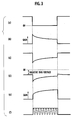
- the modulation pulse exemplarily shown in Fig. 3(a)
- the modulation pulse is delivered to the switching circuit 13 and the pulse differentiating circuit 14.
- the switching circuit 13 switches the output voltage of the positive bias power supply 21 in response to the modulation pulse. Then, during a time period corresponding to a pulse width, the output voltage of the positive bias supply 21 is passed and outputted to the FETs 10 to 12.
- the pulse differentiating circuit 14 differentiates the modulation pulse, applied through the pulse input terminal 18, by a given time constant.
- the time constant is determined based on the thermal time constants of the FETs 10 and 11. That is, during pulse amplifying operations of the FETs 10 and 11, the temperatures of respective channels increase and, as exemplarily shown in Fig. 3(b), amplification gains of the FETs 10 and 11 decrease in one pulse from a leading edge of the pulse toward a trailing edge thereof in dependence on the thermal time constants.
- the pulse differentiating circuit 14 differentiates the modulation pulse to generate a voltage waveform, as exemplarily shown in Fig. 3(c), which corresponds to variation in the amplification gain as shown in Fig 3(b) in terms of time, and which in turn is transmitted to the adder circuit 15.
- the adder circuit 15 adds the differentiated waveform, delivered from the pulse differentiating circuit 14, and the output voltage of the negative bias power supply 22 applied through the high potential terminal 20.
- an output voltage has a waveform in which the voltage varies in phase in dependence on the thermal time constants of the FETs 10 and 11 from the leading edge of the modulation pulse toward the trailing edge thereof. This voltage waveform is applied to the inputs of the FETs 10 and 11 as the input bias voltage, respectively.
- the FETs 10 and 11 Due to variation in the input bias voltage, the FETs 10 and 11 cause the amplification gain to vary in a manner as shown in Fig. 3(e). That is, the amplification gain varies to compensate for variation in the amplification gain resulting from the thermal time constant in one pulse as shown in Fig. 3(b).
- the high frequency signal supplied from the signal input terminal 16 is pulse amplified in each stage of the FETs 10 to 12 that operate based on a biased condition determined in a such a manner as mentioned above.
- the input bias voltage transmitted to FETs 10 and 11 is determined to vary based on the thermal time constants of the associated FETs to suppress variation in the amplification gain in one pulse as shown in Fig 3(f).
- a resulting output occurs with reduced amplitude fluctuation in one pulse as shown in Fig. 3(f) and is delivered to a subsequent stage.
- the high frequency signal is amplified in the final stage FET 12 under an optimum input signal condition and biased condition to be outputted from the signal output terminal 17 as a transmission pulse signal.
- the input bias voltage to be applied to the FETs is varied in dependence on the thermal time constants of the FETs used as the respective power amplifier elements to compensate for variation in the amplification gain in terms of time in one pulse during pulse amplifying operation. This enables the pulse amplification to be achieved at a stabilized gain, thereby making it possible to eliminate amplitude fluctuation of the pulse signal in one pulse subsequent to the amplification step.
- the pulse power amplifier 1 includes the three cascaded stages and controls the input bias voltage for the initial stage and second stage
- the present invention is not limited to particular number of stages and a particular amplifying stage delivered input bias voltage can be appropriately selected in accordance with the allocation of the amplification gain.
- a pulsed power amplifier that includes power amplifier elements comprised of bipolar transistors, which are connected in cascaded multiple stages with a base electrode serving as an input terminal, a collector electrode serving as an output terminal and an emitter electrode serving as a common terminal, can achieve the same advantageous effects as those set forth above.
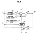
- Fig. 4 is a block diagram illustrating a pulsed power amplifier of a second embodiment according to the present invention.
- a pulse power amplifier of the second embodiment compensates amplitude variation in one pulse of a pulse signal based on the amount of attenuation of a variable attenuator. The amount of attenuation is varied in response to the thermal time constants of the FETs.
- description is made with reference to Fig. 4.
- a pulsed power amplifier 2 includes the FETs 10 to 12, the switching circuit 13, the pulse differentiating circuit 14, an attenuator control circuit 23 and a variable attenuator 24.
- the pulse power amplifier 2 further includes the signal input terminal 16, the signal output terminal 17, the pulse input terminal 18, the high potential terminal 19 and the low potential terminal 20.
- the FETs 10 to 12 have gate electrodes serving as input terminals, drain electrodes serving as output terminals and the source electrodes serving as common terminals, respectively.
- the FETs 10 to 12 are connected in a cascade to form a first stage, a second stage and a final stage, respectively.
- the gate electrode of the FET 10 is connected to the signal input terminal 16 via the variable attenuator 24, and the drain electrode of the FET 12 is connected to the signal output terminal 17.
- the switching circuit 13 switches the output of the positive bias power supply 21 based on a modulation pulse applied to the pulse input terminal 18 to transmit a positive operational power supply voltage to the FETs 10 to 12.
- the pulse differentiating circuit 14 differentiates a leading edge of the modulation pulse, applied to the pulse input terminal 18, by a given time constant. Then, a resulting differentiated signal is delivered to the attenuator control circuit 23.
- the time constant, used for differentiation as mentioned above, is determined based on the thermal time constants of the FETs 10 to 12.
- the attenuator control circuit 23 generates a control signal, in dependence on the differentiated signal delivered from the pulse differentiating circuit 14 for controlling the amount of attenuation to be achieved by the variable attenuator 24, and transmits the control signal to the variable attenuator 24.
- the variable attenuator 24 includes, for instance, a variable attenuator such as a diode which is able to continuously control the amount of attenuation.
- the variable attenuator 24 also attenuates a high frequency signal, applied through the signal input terminal 16, in dependence on the control signal delivered from the attenuator control circuit 23 to allow a resulting attenuated signal to be delivered to the FET 10.
- Connected to the low potential terminal 20 is a fixed negative bias power supply 22, by which a negative bias voltage required for the FETs 10 to 12 is supplied.
- the output voltages of the positive bias power supply 21 and the negative bias power supply 22 are supplied through the high potential terminal 19 and the low potential terminal 20, respectively.
- the signal input terminal 16 is applied with a high frequency signal that forms a source signal of a transmission pulse.
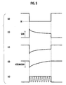
- a modulation pulse exemplarily shown in Fig. 5(a)
- the modulation pulse is delivered to the switching circuit 13 and the pulse differentiating circuit 14.
- the switching circuit 13 switches the output voltage of the positive bias power supply 21, supplied through the high potential terminal 19, by the modulation pulse. Then, during a period corresponding to a pulse width, the output voltage of the positive bias power supply 21 is passed and outputted to the FETs 10 to 12.
- the pulse differentiating circuit 14 differentiates the modulation pulse, delivered through the pulse input terminal 18, by a given time constant.
- the time constant is determined based on the thermal time constants of the FETs 10 to 12. That is, due to increases in channel temperature of the FETs 10 to 12 during a pulsed amplifying operation, the FETs 10 to 12 operate such that the amplification gain decreases from a leading edge of the pulse toward a trailing edge thereof in one pulse in accordance with the thermal time constants of the FETs, as exemplarily shown in Fig. 5(b).
- the pulse differentiating circuit 14 By differentiating the modulation pulse, the pulse differentiating circuit 14 generates a voltage waveform, as exemplarily shown in Fig. 5(c), which corresponds to a variation in the amplification gain in terms of time and is outputted to the attenuator control circuit 23.
- the attenuator control circuit 23 Depending upon the differentiated waveform delivered from the pulse differentiating circuit 14, the attenuator control circuit 23 generates a control signal for controlling the amount of attenuation to be achieved by the variable attenuator 24.
- An example of the resulting control signal is shown in Fig. 5(d). That is, the control signal forms a signal that controls the amount of attenuation to be achieved by the variable attenuator 24 in phase from the leading edge of the modulation pulse toward the trailing edge thereof so as to cancel the variation in the amplification gain in terms of time in one pulse applied to the FETs 10 to 12.
- the resulting control signal is delivered to the variable attenuator 24.
- the variable attenuator 24 attenuates the high frequency signal, delivered from the signal input terminal 16, in accordance with the control signal.
- a level control is performed on the high frequency signal applied to the signal input terminal 16 by the variable attenuator 24. Then, the high frequency signal is pulse amplified in each stage of the FETs 10 to 12 so as to be transmitted from the signal output terminal 17.
- the variable attenuator 24 controls the amount of attenuation to be applied to the high frequency signal in response to the control signal delivered from the attenuator control circuit 23. Therefore, the first stage FET 10 is provided with the level controlled high frequency signal so as to compensate for variation in the amplification gain in one pulse and then amplified.
- the amplified high frequency signal is sequentially delivered to the subsequent stages. As a result, a transmission pulse signal, whose amplitude variation in one pulse is eliminated in a manner as exemplarily shown in Fig. 5(e), is outputted from the signal output terminal 17.
- the level of the high frequency signal to be applied to the FETs is controlled in dependence on the thermal time constants of the FETs used as the power amplifier elements to compensate variation in amplification gain in terms of time in one pulse during pulsed amplifying operation. This enables reduction in amplitude variation in one pulse of the pulse signal subsequent to amplification.
- the respective FETs connected in cascaded multiple stages perform the pulsed amplifying operation without causing an excessively large input to be present in a region that does not form a saturated area. This results in a capability of achieving an amplification characteristic with less intermodulation distortion occurring at a higher order, to provide a favorable linearity.
- the pulse power amplifier 2 includes the three cascaded stages and the variable attenuator 24 provided at the input side of the power amplifier element of the first stage, the present invention is not limited to such a particular number of stages.
- Variable attenuators may be connected to the input side of the power amplifier elements of the subsequent stage or of plural stages by appropriately allocating the amount of attenuation.
- a pulsed power amplifier that includes power amplifier elements comprised of bipolar transistors, each of which has a base electrode serving as an input terminal, a collector electrode serving as an output terminal and an emitter electrode serving as a common terminal and which are connected in cascaded multiple stages, is able to achieve the same advantageous effects as those set forth above.
Landscapes
- Engineering & Computer Science (AREA)
- Power Engineering (AREA)
- Amplifiers (AREA)
- Manipulation Of Pulses (AREA)
Abstract
Description
- This application is based upon and claims the benefit of priority from prior Japanese Patent Application P2003-389498 filed on November 19, 2003; the entire contents of which are incorporated by reference herein.
- The present invention relates to an amplifier, especially a pulse power amplifier used for a pulse radar transmission system.
- In the technical field of pulse radar transmission systems, a pulse power amplifier is applied thereto. The pulse power amplifier includes a semiconductor element, for example, a field effect transistor (FET), for amplifying electrical power. As shown in Fig. 1, a
pulse power amplifier 50 includes anFET 51, anFET 52, anFET 53, and aswitching circuit 54. Additionally, thepulse power amplifier 50 includes asignal input terminal 55, asignal output terminal 56, and apulse input terminal 57. A source signal is supplied to thesignal input terminal 55. An amplified signal is transmitted to thesignal output terminal 56. TheFETs 51 to 53 are connected in three cascaded stages. TheFETs bias power supply 60 is switched by theswitching circuit 54 in response to a modulation pulse transmitted from thepulse input terminal 57 so as to be delivered to the drain electrodes for amplifying operations. An input voltage of a negativebias power supply 61 is delivered to the gate electrodes. Then, the source signal supplied from thesignal input terminal 55 is amplified by theFETs 51 to 53, and is modulated based on the modulation pulse to be transmitted as a transmission pulse. The Japanese laid open publication (Kokai) 2001-16045 discloses equalization of saturated output power so as to keep the transmission pulse constant by varying a bias voltage supplied to a drain electrode of an FET serving as a power amplifier element. - In the related art as shown in Fig. 1, an increase of channel temperature of the
FETs 51 to 53 causes a decrease of an amplification gain. That is, amplitude in one pulse from a leading edge of the pulse toward a trailing edge thereof varies based on thermal time constants of the channel. In case of the Japanese laid open, the FETs used as the power amplifier elements are rendered operational in saturated areas to cause a drop to occur in the resulting saturated output power. Therefore, the output tends to contain intermodulation distortion at a higher order. Also, a difficulty has been encountered in obtaining an amplification characteristic with a favorable linearity. Further, due to the presence of an inability of responding to variation in the amplification gain of the FET, another difficulty has been encountered in adequately eliminating amplitude variation in one pulse during an amplifying operation using a small signal. - The present invention has been completed taking into account the circumstances, which have been stated above, and provides a pulsed power amplifier whose amplitude variation in one pulse of a pulse signal subsequent to an amplification step is eliminated to provide a favorable linearity.
- An aspect of the present invention inheres in an amplifier including a plurality of power amplifier elements connected in cascaded multiple stages, a first bias power supply, a second bias power supply, a switching circuit configured to switch a first output supplied from the first bias power supply in response to a modulation pulse so as to transmit the first output to the plurality of power amplifier elements, a pulse differentiating circuit configured to differentiate the modulation pulse by a given time constant, and an adder circuit configured to add the differentiated modulation pulse and a second output of the second bias power supply so as to transmit the differentiated modulation pulse added to the second output as an input bias voltage to at least one of the plurality of power amplifier elements except for a final stage in the cascaded multiple stages.
- Another aspect of the present invention inheres in an amplifier including a plurality of power amplifier elements connected in cascaded multiple stages, a bias power supply, a switching circuit configured to switch an output supplied from the bias power supply in response to a modulation pulse so as to transmit the output to the plurality of power amplifier elements, a pulse differentiating circuit configured to differentiate the modulation pulse by a given time constant, a variable attenuator provided on an input side of at least one of the plurality of power amplifier elements and configured to attenuate a frequency signal, and an attenuator control circuit configured to generate a control signal for controlling the amount of attenuation to be achieved by the variable attenuator.
-
- Fig. 1 is a block diagram schematically illustrating the related art.
- Fig. 2 is a block diagram schematically illustrating a pulsed power amplifier of a first embodiment according to the present invention.
- Fig. 3 is a view schematically showing pulse transmitted from each of units of the first embodiment.
- Fig. 4 is a block diagram schematically illustrating a pulsed power amplifier of a second embodiment according to the present invention
- Fig. 5 is a view schematically showing pulse transmitted from each of units of the second embodiment.
-
- Various embodiments of the present invention will be described with reference to the accompanying drawings. It is to be noted that the same or similar reference numerals are applied to the same or similar parts and elements throughout the drawings, and the description of the same or similar parts and elements will be omitted or simplified.
- In the following description specific details are set forth, such as specific materials, process and equipment in order to provide thorough understanding of the present invention. It will be apparent, however, to one skilled in the art that the present invention may be practiced without these specific details. In other instances, well-known manufacturing materials, process and equipment are not set forth in detail in order not unnecessary obscure the present invention.
- Fig. 2 is a block diagram illustrating a pulsed power amplifier of a first embodiment according to the present invention. A pulsed power amplifier includes power amplifier elements, for example, N-channel MES type FETs that are connected in three cascaded stages. As shown in Fig. 2, the
pulsed power amplifier 1 includesFETs switching circuit 13, apulse differentiating circuit 14 and anadder circuit 15. Also, the other elements include asignal input terminal 16, asignal output terminal 17, apulse input terminal 18, a highpotential terminal 19, and a lowpotential terminal 20. - The
FETs 10 to 12 have gate electrodes serving as input terminals, drain electrodes serving as output terminals and source electrodes serving as common terminals, respectively. The FETs 10, 11 and 12 serve as a first stage, a second stage and a final stage which are connected in a cascaded arrangement. Further, the gate electrode of theFET 10 and the drain electrode of theFET 12 are connected to thesignal input terminal 16 and thesignal output terminal 17, respectively. - The
switching circuit 13 switches an output supplied from a positivebias power supply 21 to the FETS 10 to 12 via the highpotential terminal 19 in response to a modulation pulse being applied to thepulse input terminal 18. - The
pulse differentiating circuit 14 differentiates a leading edge of the modulation pulse, applied through thepulse input terminal 18, by a given time constant to allow a resulting differentiated signal to be delivered to theadder circuit 15. The time constant is determined based on thermal time constants of theFETs adder circuit 15. - The
adder circuit 15 adds an output voltage of a negativebias power supply 22, applied via the lowpotential terminal 20, and the differentiated signal resulting from thepulse differentiating circuit 14, and supplies a negative bias voltage to the inputs of theFETs final stage FET 12. Also, thefinal stage FET 12 is directly supplied with the output voltage of the negativebias power supply 22, as an input negative bias voltage, via the lowpotential terminal 20. - The operation of the
pulsed power amplifier 1 is described with reference to FIGS. 2 and 3. - The output voltages of the positive
bias power supply 21 and the negativebias power supply 22 are supplied through the highpotential terminal 19 and the lowpotential terminal 20, respectively. Thesignal input terminal 16 receives a high frequency signal that forms a source signal of a transmission pulse. - When the modulation pulse, exemplarily shown in Fig. 3(a), is inputted from the
pulse input terminal 18, the modulation pulse is delivered to theswitching circuit 13 and thepulse differentiating circuit 14. Theswitching circuit 13 switches the output voltage of the positivebias power supply 21 in response to the modulation pulse. Then, during a time period corresponding to a pulse width, the output voltage of thepositive bias supply 21 is passed and outputted to theFETs 10 to 12. - Further, the
pulse differentiating circuit 14 differentiates the modulation pulse, applied through thepulse input terminal 18, by a given time constant. The time constant is determined based on the thermal time constants of theFETs FETs FETs pulse differentiating circuit 14 differentiates the modulation pulse to generate a voltage waveform, as exemplarily shown in Fig. 3(c), which corresponds to variation in the amplification gain as shown in Fig 3(b) in terms of time, and which in turn is transmitted to theadder circuit 15. - The
adder circuit 15 adds the differentiated waveform, delivered from thepulse differentiating circuit 14, and the output voltage of the negativebias power supply 22 applied through the highpotential terminal 20. After the adding operation, as shown in Fig. 3(d), an output voltage has a waveform in which the voltage varies in phase in dependence on the thermal time constants of theFETs FETs - Due to variation in the input bias voltage, the
FETs - The high frequency signal supplied from the
signal input terminal 16 is pulse amplified in each stage of theFETs 10 to 12 that operate based on a biased condition determined in a such a manner as mentioned above. The input bias voltage transmitted to FETs 10 and 11 is determined to vary based on the thermal time constants of the associated FETs to suppress variation in the amplification gain in one pulse as shown in Fig 3(f). Thus, a resulting output occurs with reduced amplitude fluctuation in one pulse as shown in Fig. 3(f) and is delivered to a subsequent stage. The high frequency signal is amplified in thefinal stage FET 12 under an optimum input signal condition and biased condition to be outputted from thesignal output terminal 17 as a transmission pulse signal. - As set forth above, with the first embodiment, the input bias voltage to be applied to the FETs is varied in dependence on the thermal time constants of the FETs used as the respective power amplifier elements to compensate for variation in the amplification gain in terms of time in one pulse during pulse amplifying operation. This enables the pulse amplification to be achieved at a stabilized gain, thereby making it possible to eliminate amplitude fluctuation of the pulse signal in one pulse subsequent to the amplification step.
- Further, no control is performed on the final stage FET that forms part of the FETs connected in cascaded multiple stages. Instead, the control is performed on a preceding stage wherein the saturated output level is not controlled but the amplification gain is controlled. Therefore, the pulse is amplified without an excessively increased input to be applied to the FETs involving the final stage, thereby making it possible to obtain an amplification characteristic with less intermodulation distortion, resulting from intermodulation occurring at a higher order, to provide a favorable linearity.
- Also, while the
pulse power amplifier 1 includes the three cascaded stages and controls the input bias voltage for the initial stage and second stage, the present invention is not limited to particular number of stages and a particular amplifying stage delivered input bias voltage can be appropriately selected in accordance with the allocation of the amplification gain. - Furthermore, a pulsed power amplifier that includes power amplifier elements comprised of bipolar transistors, which are connected in cascaded multiple stages with a base electrode serving as an input terminal, a collector electrode serving as an output terminal and an emitter electrode serving as a common terminal, can achieve the same advantageous effects as those set forth above.
- Fig. 4 is a block diagram illustrating a pulsed power amplifier of a second embodiment according to the present invention. With respect to various component parts of the second embodiment, the same component parts as those of the first embodiment shown in Fig. 2 bear like reference numerals. A pulse power amplifier of the second embodiment compensates amplitude variation in one pulse of a pulse signal based on the amount of attenuation of a variable attenuator. The amount of attenuation is varied in response to the thermal time constants of the FETs. Hereinafter, description is made with reference to Fig. 4.
- As shown in Fig. 4, a
pulsed power amplifier 2 includes theFETs 10 to 12, the switchingcircuit 13, thepulse differentiating circuit 14, anattenuator control circuit 23 and avariable attenuator 24. Thepulse power amplifier 2 further includes thesignal input terminal 16, thesignal output terminal 17, thepulse input terminal 18, the highpotential terminal 19 and the lowpotential terminal 20. - The
FETs 10 to 12 have gate electrodes serving as input terminals, drain electrodes serving as output terminals and the source electrodes serving as common terminals, respectively. TheFETs 10 to 12 are connected in a cascade to form a first stage, a second stage and a final stage, respectively. Also, the gate electrode of theFET 10 is connected to thesignal input terminal 16 via thevariable attenuator 24, and the drain electrode of theFET 12 is connected to thesignal output terminal 17. - The switching
circuit 13 switches the output of the positivebias power supply 21 based on a modulation pulse applied to thepulse input terminal 18 to transmit a positive operational power supply voltage to theFETs 10 to 12. - The
pulse differentiating circuit 14 differentiates a leading edge of the modulation pulse, applied to thepulse input terminal 18, by a given time constant. Then, a resulting differentiated signal is delivered to theattenuator control circuit 23. With the second embodiment, the time constant, used for differentiation as mentioned above, is determined based on the thermal time constants of theFETs 10 to 12. - The
attenuator control circuit 23 generates a control signal, in dependence on the differentiated signal delivered from thepulse differentiating circuit 14 for controlling the amount of attenuation to be achieved by thevariable attenuator 24, and transmits the control signal to thevariable attenuator 24. Thevariable attenuator 24 includes, for instance, a variable attenuator such as a diode which is able to continuously control the amount of attenuation. Thevariable attenuator 24 also attenuates a high frequency signal, applied through thesignal input terminal 16, in dependence on the control signal delivered from theattenuator control circuit 23 to allow a resulting attenuated signal to be delivered to theFET 10. Connected to the lowpotential terminal 20 is a fixed negativebias power supply 22, by which a negative bias voltage required for theFETs 10 to 12 is supplied. - The operation of the
pulsed power amplifier 2 is described with reference to illustrative views of FIGS. 4 and 5 mentioned above. - The output voltages of the positive
bias power supply 21 and the negativebias power supply 22 are supplied through the highpotential terminal 19 and the lowpotential terminal 20, respectively. Thesignal input terminal 16 is applied with a high frequency signal that forms a source signal of a transmission pulse. - When a modulation pulse, exemplarily shown in Fig. 5(a), is applied through the
pulse input terminal 18, the modulation pulse is delivered to the switchingcircuit 13 and thepulse differentiating circuit 14. The switchingcircuit 13 switches the output voltage of the positivebias power supply 21, supplied through the highpotential terminal 19, by the modulation pulse. Then, during a period corresponding to a pulse width, the output voltage of the positivebias power supply 21 is passed and outputted to theFETs 10 to 12. - The
pulse differentiating circuit 14 differentiates the modulation pulse, delivered through thepulse input terminal 18, by a given time constant. The time constant is determined based on the thermal time constants of theFETs 10 to 12. That is, due to increases in channel temperature of theFETs 10 to 12 during a pulsed amplifying operation, theFETs 10 to 12 operate such that the amplification gain decreases from a leading edge of the pulse toward a trailing edge thereof in one pulse in accordance with the thermal time constants of the FETs, as exemplarily shown in Fig. 5(b). By differentiating the modulation pulse, thepulse differentiating circuit 14 generates a voltage waveform, as exemplarily shown in Fig. 5(c), which corresponds to a variation in the amplification gain in terms of time and is outputted to theattenuator control circuit 23. - Depending upon the differentiated waveform delivered from the
pulse differentiating circuit 14, theattenuator control circuit 23 generates a control signal for controlling the amount of attenuation to be achieved by thevariable attenuator 24. An example of the resulting control signal is shown in Fig. 5(d). That is, the control signal forms a signal that controls the amount of attenuation to be achieved by thevariable attenuator 24 in phase from the leading edge of the modulation pulse toward the trailing edge thereof so as to cancel the variation in the amplification gain in terms of time in one pulse applied to theFETs 10 to 12. The resulting control signal is delivered to thevariable attenuator 24. Thevariable attenuator 24 attenuates the high frequency signal, delivered from thesignal input terminal 16, in accordance with the control signal. - A level control is performed on the high frequency signal applied to the
signal input terminal 16 by thevariable attenuator 24. Then, the high frequency signal is pulse amplified in each stage of theFETs 10 to 12 so as to be transmitted from thesignal output terminal 17. Thevariable attenuator 24 controls the amount of attenuation to be applied to the high frequency signal in response to the control signal delivered from theattenuator control circuit 23. Therefore, thefirst stage FET 10 is provided with the level controlled high frequency signal so as to compensate for variation in the amplification gain in one pulse and then amplified. The amplified high frequency signal is sequentially delivered to the subsequent stages. As a result, a transmission pulse signal, whose amplitude variation in one pulse is eliminated in a manner as exemplarily shown in Fig. 5(e), is outputted from thesignal output terminal 17. - As set forth above, with the second embodiment, the level of the high frequency signal to be applied to the FETs is controlled in dependence on the thermal time constants of the FETs used as the power amplifier elements to compensate variation in amplification gain in terms of time in one pulse during pulsed amplifying operation. This enables reduction in amplitude variation in one pulse of the pulse signal subsequent to amplification.
- Further, the respective FETs connected in cascaded multiple stages perform the pulsed amplifying operation without causing an excessively large input to be present in a region that does not form a saturated area. This results in a capability of achieving an amplification characteristic with less intermodulation distortion occurring at a higher order, to provide a favorable linearity.
- Also, while the
pulse power amplifier 2 includes the three cascaded stages and thevariable attenuator 24 provided at the input side of the power amplifier element of the first stage, the present invention is not limited to such a particular number of stages. Variable attenuators may be connected to the input side of the power amplifier elements of the subsequent stage or of plural stages by appropriately allocating the amount of attenuation. - Moreover, a pulsed power amplifier that includes power amplifier elements comprised of bipolar transistors, each of which has a base electrode serving as an input terminal, a collector electrode serving as an output terminal and an emitter electrode serving as a common terminal and which are connected in cascaded multiple stages, is able to achieve the same advantageous effects as those set forth above.
- The present invention may be embodied in other specific forms without departing from the spirit or essential characteristics thereof. The embodiments are therefore to be considered in all respects as illustrative and not restrictive, the scope of the present invention being indicated by the appended claims rather than by the foregoing description, and all changes which come within the meaning and range of equivalency of the claims are therefore intended to be embraced therein.
Claims (8)
- An amplifier comprising:a plurality of power amplifier elements connected in cascaded multiple stages;a first bias power supply;a second bias power supply;a switching circuit configured to switch a first output supplied from the first bias power supply in response to a modulation pulse so as to transmit the first output to the plurality of power amplifier elements;a pulse differentiating circuit configured to differentiate the modulation pulse by a given time constant; andan adder circuit configured to add the differentiated modulation pulse and a second output of the second bias power supply so as to transmit the differentiated modulation pulse added to the second output as an input bias voltage to at least one of the plurality of power amplifier elements except for a final stage in the cascaded multiple stages.
- The amplifier of claim 1, wherein the plurality of power amplifier elements is a plurality of field-effect transistors including gate electrodes serving as input terminals, drain electrodes serving as output terminals and source electrodes serving as common terminals, respectively.
- The amplifier of claim 1, wherein the plurality of power amplifier elements is a plurality of bipolar transistors including base electrodes serving as input terminals, collector electrodes serving as output terminals and emitter electrodes serving as common terminals, respectively.
- The amplifier of any one of claims 1 to 3, wherein the given time constant is determined based on a thermal time constant of at least one of the plurality of power amplifier elements provided with the input bias voltage from the adder circuit thereto.
- An amplifier comprising:a plurality of power amplifier elements connected in cascaded multiple stages;a bias power supply;a switching circuit configured to switch an output supplied from the bias power supply in response to a modulation pulse so as to transmit the output to the plurality of power amplifier elements;a pulse differentiating circuit configured to differentiate the modulation pulse by a given time constant;a variable attenuator provided on an input side of at least one of the plurality of power amplifier elements and configured to attenuate a frequency signal; andan attenuator control circuit configured to control the amount of attenuation to be achieved by the variable attenuator based on the differentiated modulation pulse.
- The amplifier of claim 5, wherein the plurality of power amplifier elements is a plurality of field-effect transistors including gate electrodes serving as input terminals, drain electrodes serving as output terminals and source electrodes serving as common terminals, respectively.
- The amplifier of claim 5, wherein the plurality of power amplifier elements is a plurality of bipolar transistors including base electrodes serving as input terminals, collector electrodes serving as output terminals and emitter electrodes serving as common terminals, respectively.
- The amplifier of any one of claims 5 to 7, wherein the given time constant is determined based on a thermal time constant of at least one of the plurality of power amplifier elements.
Applications Claiming Priority (2)
| Application Number | Priority Date | Filing Date | Title |
|---|---|---|---|
| JP2003389498A JP4707319B2 (en) | 2003-11-19 | 2003-11-19 | Pulse power amplifier |
| JP2003389498 | 2003-11-19 |
Publications (2)
| Publication Number | Publication Date |
|---|---|
| EP1538743A1 true EP1538743A1 (en) | 2005-06-08 |
| EP1538743B1 EP1538743B1 (en) | 2008-02-27 |
Family
ID=34463760
Family Applications (1)
| Application Number | Title | Priority Date | Filing Date |
|---|---|---|---|
| EP04255037A Expired - Lifetime EP1538743B1 (en) | 2003-11-19 | 2004-08-20 | Amplifier |
Country Status (3)
| Country | Link |
|---|---|
| US (1) | US7123089B2 (en) |
| EP (1) | EP1538743B1 (en) |
| JP (1) | JP4707319B2 (en) |
Cited By (3)
| Publication number | Priority date | Publication date | Assignee | Title |
|---|---|---|---|---|
| EP1938451A1 (en) * | 2005-08-30 | 2008-07-02 | Thales | Device and method for amplifying pulsed rf signals |
| GB2463702A (en) * | 2008-09-23 | 2010-03-24 | Technetix Group Ltd | An amplifier system for cable television network which has a power delay device |
| KR101089955B1 (en) | 2009-12-28 | 2011-12-05 | 삼성전기주식회사 | Power amplifier |
Families Citing this family (5)
| Publication number | Priority date | Publication date | Assignee | Title |
|---|---|---|---|---|
| JP5183051B2 (en) * | 2006-09-25 | 2013-04-17 | 東芝テリー株式会社 | High frequency power amplifier circuit |
| JP2011254438A (en) * | 2010-06-04 | 2011-12-15 | Toshiba Corp | Pulse power amplifier |
| JP5541114B2 (en) * | 2010-11-25 | 2014-07-09 | 三菱電機株式会社 | Power amplifier and MMIC using the same |
| JP5422598B2 (en) * | 2011-04-25 | 2014-02-19 | 株式会社東芝 | Pulse power amplifier |
| US9712125B2 (en) * | 2015-02-15 | 2017-07-18 | Skyworks Solutions, Inc. | Power amplification system with shared common base biasing |
Citations (4)
| Publication number | Priority date | Publication date | Assignee | Title |
|---|---|---|---|---|
| JPS5549044A (en) * | 1978-10-04 | 1980-04-08 | Hitachi Ltd | Sound muting control circuit |
| JPS5937737A (en) * | 1982-08-25 | 1984-03-01 | Toshiba Corp | Automatic controlling circuit of volume of received voice |
| US20010014593A1 (en) * | 1999-02-09 | 2001-08-16 | Mccune Earl | High-efficiency modulating rf amplifier |
| US20020140503A1 (en) * | 2001-03-27 | 2002-10-03 | Mobile Communications Tokyo Inc. | High-frequency power amplifying apparatus |
Family Cites Families (8)
| Publication number | Priority date | Publication date | Assignee | Title |
|---|---|---|---|---|
| JPH03111017U (en) * | 1990-03-01 | 1991-11-14 | ||
| EP0489276B1 (en) * | 1990-12-03 | 1995-06-28 | Siemens Aktiengesellschaft | Modulation device for a high-frequency power amplifier |
| JPH0760978B2 (en) * | 1990-12-28 | 1995-06-28 | 日本無線株式会社 | Power amplifier |
| JPH08116219A (en) * | 1994-10-14 | 1996-05-07 | Mitsubishi Electric Corp | Power amplifier with temperature compensation circuit |
| JPH11274870A (en) * | 1998-03-20 | 1999-10-08 | Fujitsu Quantum Device Kk | High frequency circuit device |
| JP2000269748A (en) * | 1999-03-19 | 2000-09-29 | Japan Radio Co Ltd | High frequency pulse power amplifier |
| JP3792442B2 (en) * | 1999-06-29 | 2006-07-05 | 株式会社東芝 | Bias circuit |
| JP2001284995A (en) * | 2000-03-31 | 2001-10-12 | Toshiba Corp | Microwave pulse power amplifier |
-
2003
- 2003-11-19 JP JP2003389498A patent/JP4707319B2/en not_active Expired - Lifetime
-
2004
- 2004-08-20 EP EP04255037A patent/EP1538743B1/en not_active Expired - Lifetime
- 2004-08-31 US US10/929,524 patent/US7123089B2/en not_active Expired - Lifetime
Patent Citations (4)
| Publication number | Priority date | Publication date | Assignee | Title |
|---|---|---|---|---|
| JPS5549044A (en) * | 1978-10-04 | 1980-04-08 | Hitachi Ltd | Sound muting control circuit |
| JPS5937737A (en) * | 1982-08-25 | 1984-03-01 | Toshiba Corp | Automatic controlling circuit of volume of received voice |
| US20010014593A1 (en) * | 1999-02-09 | 2001-08-16 | Mccune Earl | High-efficiency modulating rf amplifier |
| US20020140503A1 (en) * | 2001-03-27 | 2002-10-03 | Mobile Communications Tokyo Inc. | High-frequency power amplifying apparatus |
Non-Patent Citations (2)
| Title |
|---|
| PATENT ABSTRACTS OF JAPAN vol. 004, no. 083 (E - 015) 14 June 1980 (1980-06-14) * |
| PATENT ABSTRACTS OF JAPAN vol. 008, no. 127 (E - 250) 14 June 1984 (1984-06-14) * |
Cited By (3)
| Publication number | Priority date | Publication date | Assignee | Title |
|---|---|---|---|---|
| EP1938451A1 (en) * | 2005-08-30 | 2008-07-02 | Thales | Device and method for amplifying pulsed rf signals |
| GB2463702A (en) * | 2008-09-23 | 2010-03-24 | Technetix Group Ltd | An amplifier system for cable television network which has a power delay device |
| KR101089955B1 (en) | 2009-12-28 | 2011-12-05 | 삼성전기주식회사 | Power amplifier |
Also Published As
| Publication number | Publication date |
|---|---|
| US20050104656A1 (en) | 2005-05-19 |
| JP2005151442A (en) | 2005-06-09 |
| EP1538743B1 (en) | 2008-02-27 |
| JP4707319B2 (en) | 2011-06-22 |
| US7123089B2 (en) | 2006-10-17 |
Similar Documents
| Publication | Publication Date | Title |
|---|---|---|
| EP1563600B1 (en) | Systems and methods of dynamic bias switching for radio frequency power amplifiers | |
| US5886575A (en) | Apparatus and method for amplifying a signal | |
| EP0139078B1 (en) | Amplifier transistor circuit | |
| EP0673112B1 (en) | Power amplifier and power amplification method | |
| CN100521509C (en) | Gain changeable amplifier | |
| US8471637B2 (en) | Variable gain amplifier | |
| EP1176710A2 (en) | A predistortion circuit | |
| US7649411B2 (en) | Segmented power amplifier | |
| JPH05259765A (en) | High frequency high output amplifier | |
| US7123089B2 (en) | Power amplifier with pulse differentiating circuit | |
| US6600377B2 (en) | Gain control amplifier | |
| KR100631973B1 (en) | Variable gain broadband amplifier | |
| JP2000174559A (en) | Microwave power amplifier | |
| GB2276052A (en) | Gain control for multi-stage cell-phone amplifier | |
| KR19990042066A (en) | Variable gain amplifier | |
| US5999047A (en) | Linearizer for use with RF power amplifiers | |
| US6466095B1 (en) | Power amplifier | |
| EP2573937A1 (en) | Power amplifier module having bias circuit | |
| JPH09172338A (en) | Method and apparatus for linearizing the amplification and phase response of traveling wave tubes and semiconductor amplifiers at different output levels | |
| US4980584A (en) | Multi-stage wideband successive detection logarithmic amplifier | |
| US5373250A (en) | MESFET power amplifier and its power supply unit, in particular for microwave signal amplification on board a satellite | |
| JPH09266427A (en) | Multistage amplifier | |
| JP3565667B2 (en) | Variable gain semiconductor circuit | |
| US6693492B2 (en) | Variable gain low-noise amplifier and method | |
| JPH10284959A (en) | Amplifier stage circuit |
Legal Events
| Date | Code | Title | Description |
|---|---|---|---|
| PUAI | Public reference made under article 153(3) epc to a published international application that has entered the european phase |
Free format text: ORIGINAL CODE: 0009012 |
|
| 17P | Request for examination filed |
Effective date: 20040902 |
|
| AK | Designated contracting states |
Kind code of ref document: A1 Designated state(s): AT BE BG CH CY CZ DE DK EE ES FI FR GB GR HU IE IT LI LU MC NL PL PT RO SE SI SK TR |
|
| AX | Request for extension of the european patent |
Extension state: AL HR LT LV MK |
|
| AKX | Designation fees paid |
Designated state(s): FR GB |
|
| REG | Reference to a national code |
Ref country code: DE Ref legal event code: 8566 |
|
| 17Q | First examination report despatched |
Effective date: 20061113 |
|
| GRAP | Despatch of communication of intention to grant a patent |
Free format text: ORIGINAL CODE: EPIDOSNIGR1 |
|
| GRAS | Grant fee paid |
Free format text: ORIGINAL CODE: EPIDOSNIGR3 |
|
| GRAA | (expected) grant |
Free format text: ORIGINAL CODE: 0009210 |
|
| AK | Designated contracting states |
Kind code of ref document: B1 Designated state(s): FR GB |
|
| REG | Reference to a national code |
Ref country code: GB Ref legal event code: FG4D |
|
| ET | Fr: translation filed | ||
| PLBE | No opposition filed within time limit |
Free format text: ORIGINAL CODE: 0009261 |
|
| STAA | Information on the status of an ep patent application or granted ep patent |
Free format text: STATUS: NO OPPOSITION FILED WITHIN TIME LIMIT |
|
| 26N | No opposition filed |
Effective date: 20081128 |
|
| REG | Reference to a national code |
Ref country code: GB Ref legal event code: 746 Effective date: 20090717 |
|
| REG | Reference to a national code |
Ref country code: FR Ref legal event code: PLFP Year of fee payment: 13 |
|
| REG | Reference to a national code |
Ref country code: FR Ref legal event code: PLFP Year of fee payment: 14 |
|
| REG | Reference to a national code |
Ref country code: FR Ref legal event code: PLFP Year of fee payment: 15 |
|
| PGFP | Annual fee paid to national office [announced via postgrant information from national office to epo] |
Ref country code: GB Payment date: 20230629 Year of fee payment: 20 |
|
| PGFP | Annual fee paid to national office [announced via postgrant information from national office to epo] |
Ref country code: FR Payment date: 20230703 Year of fee payment: 20 |
|
| REG | Reference to a national code |
Ref country code: GB Ref legal event code: PE20 Expiry date: 20240819 |
|
| PG25 | Lapsed in a contracting state [announced via postgrant information from national office to epo] |
Ref country code: GB Free format text: LAPSE BECAUSE OF EXPIRATION OF PROTECTION Effective date: 20240819 |
|
| PG25 | Lapsed in a contracting state [announced via postgrant information from national office to epo] |
Ref country code: GB Free format text: LAPSE BECAUSE OF EXPIRATION OF PROTECTION Effective date: 20240819 |