EP1536497A2 - Method of manufacturing organic electroluminescent panel, manufacturing apparatus of organic electroluminescent panel, and organic electroluminescent panel - Google Patents
Method of manufacturing organic electroluminescent panel, manufacturing apparatus of organic electroluminescent panel, and organic electroluminescent panel Download PDFInfo
- Publication number
- EP1536497A2 EP1536497A2 EP04027988A EP04027988A EP1536497A2 EP 1536497 A2 EP1536497 A2 EP 1536497A2 EP 04027988 A EP04027988 A EP 04027988A EP 04027988 A EP04027988 A EP 04027988A EP 1536497 A2 EP1536497 A2 EP 1536497A2
- Authority
- EP
- European Patent Office
- Prior art keywords
- vapor
- manufacturing
- organic
- deposition mask
- glass substrate
- Prior art date
- Legal status (The legal status is an assumption and is not a legal conclusion. Google has not performed a legal analysis and makes no representation as to the accuracy of the status listed.)
- Withdrawn
Links
Images




Classifications
-
- H—ELECTRICITY
- H05—ELECTRIC TECHNIQUES NOT OTHERWISE PROVIDED FOR
- H05B—ELECTRIC HEATING; ELECTRIC LIGHT SOURCES NOT OTHERWISE PROVIDED FOR; CIRCUIT ARRANGEMENTS FOR ELECTRIC LIGHT SOURCES, IN GENERAL
- H05B33/00—Electroluminescent light sources
- H05B33/10—Apparatus or processes specially adapted to the manufacture of electroluminescent light sources
-
- C—CHEMISTRY; METALLURGY
- C23—COATING METALLIC MATERIAL; COATING MATERIAL WITH METALLIC MATERIAL; CHEMICAL SURFACE TREATMENT; DIFFUSION TREATMENT OF METALLIC MATERIAL; COATING BY VACUUM EVAPORATION, BY SPUTTERING, BY ION IMPLANTATION OR BY CHEMICAL VAPOUR DEPOSITION, IN GENERAL; INHIBITING CORROSION OF METALLIC MATERIAL OR INCRUSTATION IN GENERAL
- C23C—COATING METALLIC MATERIAL; COATING MATERIAL WITH METALLIC MATERIAL; SURFACE TREATMENT OF METALLIC MATERIAL BY DIFFUSION INTO THE SURFACE, BY CHEMICAL CONVERSION OR SUBSTITUTION; COATING BY VACUUM EVAPORATION, BY SPUTTERING, BY ION IMPLANTATION OR BY CHEMICAL VAPOUR DEPOSITION, IN GENERAL
- C23C14/00—Coating by vacuum evaporation, by sputtering or by ion implantation of the coating forming material
- C23C14/04—Coating on selected surface areas, e.g. using masks
- C23C14/042—Coating on selected surface areas, e.g. using masks using masks
-
- H—ELECTRICITY
- H10—SEMICONDUCTOR DEVICES; ELECTRIC SOLID-STATE DEVICES NOT OTHERWISE PROVIDED FOR
- H10K—ORGANIC ELECTRIC SOLID-STATE DEVICES
- H10K71/00—Manufacture or treatment specially adapted for the organic devices covered by this subclass
- H10K71/10—Deposition of organic active material
- H10K71/16—Deposition of organic active material using physical vapour deposition [PVD], e.g. vacuum deposition or sputtering
- H10K71/164—Deposition of organic active material using physical vapour deposition [PVD], e.g. vacuum deposition or sputtering using vacuum deposition
-
- H—ELECTRICITY
- H10—SEMICONDUCTOR DEVICES; ELECTRIC SOLID-STATE DEVICES NOT OTHERWISE PROVIDED FOR
- H10K—ORGANIC ELECTRIC SOLID-STATE DEVICES
- H10K71/00—Manufacture or treatment specially adapted for the organic devices covered by this subclass
- H10K71/10—Deposition of organic active material
- H10K71/16—Deposition of organic active material using physical vapour deposition [PVD], e.g. vacuum deposition or sputtering
- H10K71/166—Deposition of organic active material using physical vapour deposition [PVD], e.g. vacuum deposition or sputtering using selective deposition, e.g. using a mask
-
- H—ELECTRICITY
- H10—SEMICONDUCTOR DEVICES; ELECTRIC SOLID-STATE DEVICES NOT OTHERWISE PROVIDED FOR
- H10K—ORGANIC ELECTRIC SOLID-STATE DEVICES
- H10K71/00—Manufacture or treatment specially adapted for the organic devices covered by this subclass
Definitions
- the present invention relates to a method of manufacturing an organic electro luminescence (hereinafter, it is referred to as organic EL) panel, a manufacturing apparatus of an organic EL panel, and an organic EL panel, and particularly to a method of manufacturing an organic EL panel that can form an organic EL layer with high accuracy, a manufacturing apparatus of an organic EL panel for implementing this manufacturing method, and an organic EL panel manufactured with this manufacturing apparatus.
- organic EL organic electro luminescence
- a full-color organic EL display panel when vapor-depositing light-emitting layers of red, green and blue, three vacuum chambers for vapor-depositing materials corresponding to each color are prepared, and thus a full-color organic EL display panel is manufactured inside these vacuum chambers by using a metal mask whose area is larger and thickness is thinner than those of the organic EL display panel.
- a vapor-deposition mask for vapor-depositing light-emitting layers and so forth is formed of a single crystal silicon wafer.
- the vapor-deposition mask composed of a single crystal silicon wafer is formed by using semiconductor manufacturing techniques such as photolithography and dry etching, and therefore is processed with high accuracy.
- a vapor-deposition mask composed of a single crystal silicon wafer has substantially the same thermal expansion coefficient as that of a glass substrate, which is a vapor-deposited substrate. Therefore, the offset of depositing positions of light-emitting elements and so forth due to thermal expansion when depositing is not caused (for example, refer to Patent Document 1).
- a magnetic material mask or a metal mask is used as a vapor-deposition mask, and then spacers and the vapor-deposition mask are attracted by a substrate holder including a magnet. Thereby, the vapor-deposition mask is aligned with a vapor-deposited substrate with the spacers therebetween (for example, refer to Patent Document 2).
- a metal mask that is correspondingly large needs to be used.
- a metal mask has an extremely large thermal expansion coefficient compared to a glass substrate, which is a vapor-deposited substrate. Accordingly, there is a problem that the metal mask expands because of radiant heat when vapor-depositing so that the depositing positions of light-emitting layers and so forth are offset. Particularly, when a large-scale panel of 20-inches or more is fabricated, the offset of depositing positions become large cumulatively, and therefore the problem is serious.
- a magnetic material mask or a metal mask is used as a vapor-deposition mask, and spacers and the vapor-deposition mask are attracted with a magnet form the backside of a glass substrate, which is a vapor-deposited substrate.
- the vapor-deposition mask is closely contacted with the vapor-deposited substrate with a strong magnet without providing spacers as described in Patent Document 2 for example, the vapor-deposition mask is attached to the vapor-deposited substrate so that they can not be separated from each other easily.
- the present invention is intended to provide a method of manufacturing an organic EL panel by which highly accurate electro luminescence layers can be formed and in which the attachment and removal between a vapor-deposition mask and a vapor-deposited substrate are easy, a manufacturing apparatus of an organic EL panel with a simple structure for implementing the manufacturing method, and an organic EL panel manufactured with the manufacturing apparatus.
- a method of manufacturing an organic electro luminescence panel according to the present invention is a method of manufacturing an organic electro luminescence panel in which a part or all of an electro luminescence layer formed of a plurality of layers is formed by vapor-deposition using a vapor-deposition mask.
- the method comprises: disposing the vapor-deposition mask on a given position on a vapor-deposited substrate when vapor-depositing; and pressing the vapor-deposited substrate dynamically so as to make the vapor-deposition mask contact the vapor-deposited substrate closely.
- a vapor-deposition mask is contacted with a vapor-deposited substrate closely by pressing the vapor-deposited substrate dynamically, a gap is not generated between the vapor-deposition mask and the vapor-deposited substrate when vapor-depositing so that the accuracy of vapor-deposition pattern can be enhanced.
- the vapor-deposited substrate is classical-dynamically pressed without using magnetic force and electric force so as to be contacted with the vapor-deposition mask closely, it is avoided that the vapor-deposition mask attaches to the vapor-deposited substrate and they are never separated from each other.
- one weight or a plurality of weights is used as means for dynamically pressing. If one weight or a plurality of weights is used as a means for dynamically pressing, a vapor-deposition mask is closely contacted with a vapor-deposited substrate easily, and furthermore highly accurate electro luminescence layers can be formed with a simple manufacturing apparatus. Moreover, if a plurality of weights whose size is smaller than that of the vapor-deposited substrate, even when there are variations in the flatness of the vapor-deposited substrate, the vapor-deposition mask is closely contacted with the vapor-deposited substrate easily.
- the means for dynamically pressing includes one elastic body or a plurality of elastic bodies, and presses the vapor-deposited substrate via the elastic body.
- the means for dynamically pressing includes one elastic body or a plurality of elastic bodies, and presses the vapor-deposited substrate elastically with the elastic body. Therefore, the vapor-deposited substrate can be prevented from being damaged. In addition, even when there are variations in the flatness of the vapor-deposited substrate, the vapor-deposition mask is closely contacted with the vapor-deposited substrate accurately.
- a plunger pin is attached to the elastic body, the plunger pin being brought into contact with the vapor-deposited substrate so as to press the vapor-deposited substrate. Since a plunger pin is attached to the elastic body, even when there are variations in the flatness of the vapor-deposited substrate, the vapor-deposition mask is closely contacted with the vapor-deposited substrate accurately. If a plunger pin that moves only along a specific direction (vertical direction and so forth) is contacted with the vapor-deposited substrate so as to press it, for example, given positions of the vapor-deposited substrate can be pressed accurately.
- the vapor-deposition mask is composed of single crystal silicon for which given processing is carried out.
- the vapor-deposition mask composed of single crystal silicon, which is not a metal or magnetic material, can be used.
- the vapor-deposition mask is formed by photolithography, dry etching and so forth, a highly accurate vapor-deposition mask can be manufactured, so that a highly accurate deposition pattern can be formed.
- a manufacturing apparatus of an organic electro luminescence panel comprises the means for dynamically pressing for implementing any of the above methods of manufacturing an organic electro luminescence panel. Since the manufacturing apparatus includes the means for classical-dynamically pressing that does not use magnetic force and electric force, and press the vapor-deposited substrate with the means for pressing so as to make the vapor-deposition mask contact the vapor-deposited substrate closely. Accordingly, the accuracy of vapor-deposition pattern can be enhanced, and it is avoided that the vapor-deposition mask attaches to the vapor-deposited substrate and they are never separated from each other.
- the means for dynamically pressing is not limited to the above weights but may be such a body as can be attached to the manufacturing apparatus directly.
- An organic electro luminescence panel according to the present invention is manufactured with the above manufacturing apparatus of an organic electro luminescence panel.
- the organic electro luminescence panel is manufactured with a manufacturing apparatus including the above means for dynamically pressing, and therefore has a highly accurate vapor-deposition pattern of electro luminescence layers and has less defect and damage.
- FIG. 1 is a conceptual diagram showing a manufacturing method and a manufacturing apparatus of an organic EL panel according to a first embodiment of the present invention.
- FIG. 1 shows a longitudinal section of a manufacturing apparatus of an organic EL panel.
- a vapor-deposition chamber 1 which is a manufacturing apparatus of an organic EL panel, is used for vacuum deposition for example, and the inside thereof is hermetically sealed.
- a vapor-deposition source 2 is provided on the bottom side of inside of the vapor-deposition chamber 1.
- a vapor-deposition mask 3 formed by carrying out given processing for single crystal silicon, for example, with photolithography and etching and so forth is placed above the vapor-deposition source 2 inside the vapor-deposition chamber 1.
- Apertures 3a with a given shape are formed in the vapor-deposition mask 3 by etching and so forth.
- the apertures 3a may have the conformation of a number of dot shapes formed corresponding to each pixel of a completed organic EL panel for example. Otherwise, a plurality of apertures 3a of a slot shape may be formed in order to carry out vapor-deposition for pixels of one line arranged vertically or horizontally in a lump.
- the glass substrate 4 is loaded inside the vapor-deposition chamber 1 before the deposition process, and then is accurately placed on a given position of the top surface of the vapor-deposition mask 3 by an alignment means (not shown).
- wires composed of ITO and so forth, and part of electro luminescence layers (to be described later) in some case, are previously formed on the surface on the lower surface side (the side contacting the vapor-deposition mask 3) of the glass substrate 4.
- weights 5 which are means for dynamically pressing, are disposed on the top surface of the glass substrate 4. While FIG. 1 shows that a plurality of weights 5 is disposed, only one weight of a flat plate shape may be disposed for example. These weights 5 press the glass substrate 4 by means of gravity without using magnetic force and electric force so as to make the vapor-deposition mask 3 contact the glass substrate 4 closely.
- the means for dynamically pressing in the present invention refers to a means for pressing not by magnetic force and electric force but by force of classical dynamics, and further refers to the weight 5 shown in the first embodiment, a means for mechanically pressing shown in a third embodiment to be described later, or the like.
- vapor-deposited materials are evaporated from the vapor-deposition source 2 so as to be deposited on the glass substrate 4, and thus part or all of electro luminescence layers such as light-emitting layers are formed.
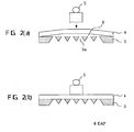
- FIG. 2 is a conceptual diagram magnified about parts of the vapor-deposition mask 3, the glass substrate 4, and the weights 5 of FIG. 1.
- FIG. 2 also shows a longitudinal section of these parts similarly to FIG. 1. Here, only one weight 5 is shown for convenience.
- the glass substrate 4 which has been loaded inside the vapor-deposition chamber 1 and has been placed on a given position on the top surface of the vapor-deposition mask 3 by the alignment means, bends considerably because of surface stresses and so forth, and therefore a gap 6 is generated between the vapor-deposition mask 3 and the glass substrate 4.
- the deposited material enters the gap 6 and thus the material is deposited on a part that should be blocked by the vapor-deposition mask normally, so that the accuracy of deposition pattern is lowered.
- the glass substrate 4 is pressed by disposing the weights 5, which are means for dynamically pressing, on the top surface of the glass substrate 4, and thereby the vapor-deposition mask 3 is contacted with the glass substrate 4 closely. This substantially eliminates the gap 6. Therefore, the vapor-deposited materials can be deposited on a given position so that the accuracy of deposition pattern can be enhanced.
- the vapor-deposition mask 3 can be contacted with the glass substrate 4 closely (refer to FIG. 1).
- the glass substrate is taken outside, and then the next glass substrate 4 is loaded inside the vapor-deposition chamber 1 and vapor-deposition is carried out.
- the flatness (extent of bending) of each glass substrate 4 often involves some variations.
- FIGs. 3, 4 and 5 are schematic diagrams showing the processes from the process of loading the glass substrate 4 into the vapor-deposition chamber 1 to the process of vapor-depositing in the first embodiment.
- FIGs. 3, 4 and 5 show longitudinal sections of the manufacturing apparatus of an organic EL panel similarly to FIG. 1, and show the more specific structure of the manufacturing apparatus of an organic EL panel than FIG.1.
- the glass substrate 4 is loaded above the vapor-deposition mask 3 inside the vapor-deposition chamber 1 from an opening 8 for loading a glass substrate of the vapor-deposition chamber 1.
- anodes composed of ITO and so forth has been already formed on the lower surface of the glass substrate 4 at this point.
- the weights 5 are lifted up above the vapor-deposition mask 3 and the glass substrate 4 by a lifting and lowering means 9 so as not to collide with the glass substrate 4.
- the weights 5 are hung by a wire 10.
- a shutter 11 of the vapor-deposition source 2 is closed and the vapor-deposition source 2 does not heat the vapor-deposited material.
- the above alignment means (not shown) is used to load the glass substrate 4 inside the vapor-deposition chamber 1.
- the glass substrate 4 is accurately deposited on a given position on the top surface of the vapor-deposition mask 3 by the alignment means (not shown). At this time, the glass substrate 4 is disposed on the vapor-deposition mask 3 so as to contact the vapor-deposition mask 3. At this point, the weights 5 are still lifted up above the vapor-deposition mask 3 and the glass substrate 4 by the lifting and lowering means 9, and the shutter 11 is still closed. Then, in the process of FIG. 5, the weights 5 are disposed on the top surface of the glass substrate 4 by the lifting and lowering means 9. The glass substrate 4 is pressed by the gravity acting on the weights 5, and thereby the vapor-deposition mask 3 is contacted with the glass substrate 4 closely.
- the lifting and lowering means 9 may be controlled with an operation panel (not shown) operated by an operator. Otherwise, the weights 5 may be automatically lifted and lowered by the lifting and lowering means 9.
- the opening 8 for loading a glass substrate is shut off by an openable door (not shown) and then the shutter 11 is opened. Then, the vapor-deposition source 2 is heated to evaporate the vapor-deposited materials, and thereby carrying out vapor-deposition of electro luminescence layers such as light-emitting layers. After the vapor-deposition is completed, the glass substrate 4 is taken outside the vapor-deposition chamber 1.
- the glass substrate 4 which is a vapor-deposited substrate, is pressed by the weights 5, and thereby the vapor-deposition mask 3 is contacted with the glass substrate 4 closely. Therefore, when depositing, the gap 6 is not generated between the vapor-deposition mask 3 and the glass substrate 4 so that the accuracy of deposition pattern can be enhanced.
- the glass substrate 4 is classical-dynamically pressed without using magnetic force and electric force so as to be contacted with the vapor-deposition mask 3 closely, it is avoided that the vapor-deposition mask 3 attaches to the glass substrate 4 and they are never separated from each other.
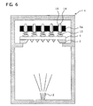
- FIG. 6 is a schematic diagram showing a manufacturing apparatus of an organic EL panel according to a second embodiment of the present invention.
- FIG. 6 shows a longitudinal section of a manufacturing apparatus of an organic EL panel similarly to FIG. 1 of the first embodiment.
- the manufacturing apparatus of an organic EL panel according to the second embodiment uses a weight 5a, springs 13, and plunger pins 14 as a means for dynamically pressing.
- Other features are the same as those of the manufacturing apparatus of an organic EL panel of the first embodiment, and the lifting and lowering means 9, the wire 10, and so forth of FIG. 3 are omitted.
- one weight 5a is provided above the vapor-deposition mask 3 and the glass substrate 4 inside the vapor-deposition chamber 1.
- a plurality of springs 13 as an elastic body is provided for the weight 5a, and the plunger pins 14 are attached to the springs 13.
- the plunger pins 14 moves inside tube guides 15 formed in the weight 5a only along the vertical direction. Only one spring 13 and one plunger pin 14 may be provided.
- the weight 5a coupled to the wire 10 (not shown in FIG. 6) is lowered by the lifting and lowering means ⁇ (not shown in FIG. 6).
- the plunger pins 14 are contacted with the glass substrate 4 so as to press the glass substrate 4 through the springs 13. This makes the vapor-deposition mask 3 be in close contact with the glass substrate 4.
- the glass substrate 4 may be pressed by an elastic body such as the springs 13 directly without providing the plunger pins 14.
- the glass substrate 4 may be pressed by vertically moving the weight 5a with a metal rod or the like by the driving means. Moreover, the glass substrate 4 may be pressed by using a flat plate weight instead of the weight 5a, the springs 13, and the plunger pins 14 and attaching a sponge elastic body to the lower surface of the weight.
- the weight 5a includes one or more springs 13 so as to press the glass substrate 4 elastically via the springs 13. Therefore, the glass substrate 4 is prevented from being damaged. Furthermore, even when there are variations in the flatness of the glass substrates 4, the vapor-deposition mask 3 can accurately be contacted with the glass substrate 4 closely. Moreover, since the plunger pins 14 that moves only along a specific direction are contacted with the glass substrate 4 so as to press it, a given position of the glass substrate 4 can accurately be pressed. Other effects are the same as the first embodiment.
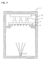
- FIG. 7 is a schematic diagram showing a manufacturing apparatus of an organic EL panel according to a third embodiment of the present invention.
- FIG. 7 shows a longitudinal section of a manufacturing apparatus of an organic EL panel similarly to FIG. 1 of the first embodiment.
- the manufacturing apparatus of an organic EL panel according to the third embodiment uses arms 17 and a driving means 18 as the means for dynamically pressing. Other features are the same as the manufacturing apparatus of an organic EL panel of the first embodiment.
- the glass substrate 4 is pressed by means of the arms 17 instead of the weights 5 in the first embodiment.
- the arms 17 move vertically by means of the driving means 18.
- the driving means 18 is provided on the top surface of inside of the vapor-deposition chamber 1, and the arms 17 are attached to the vapor-deposition chamber 1 directly.
- the arms 17 press the glass substrate 4 so as to make the vapor-deposition mask 3 be in close contact with the glass substrate 4.
- the driving means 18 may be controlled in such a manner that the arms 17 are moved while an operator monitors the position and so forth of the arms 17.
- the driving means 18 may be provided with a pressure sensor (not shown) or the like so as to be controlled automatically so that given pressure is placed on the glass substrate 4.
- the weight 5a, the springs 13, and the plunger pins 14 as shown in FIG. 6 of the second embodiment may be attached to arms such as metal rods so as to be moved by a driving means. While the arms 17 and the driving means 18 press the glass substrate 4 classical-dynamically, it will be obvious that electric forth or the like may be used as the driving force for the driving means 18 itself.
- the glass substrate 4 which is a vapor-deposited substrate, is pressed by the arms 17, and thereby the vapor-deposition mask 3 is contacted with the glass substrate 4 closely. Therefore, when depositing, the gap is not generated between the vapor-deposition mask 3 and the glass substrate 4 so that the accuracy of deposition pattern can be enhanced.
- the glass substrate 4 is pressed by the arms 17 and the driving means 18 that do not use magnetic force and electric force so as to be contacted with the vapor-deposition mask 3 closely, it is avoided that the vapor-deposition mask 3 attaches to the glass substrate 4 and they are never separated from each other.
- FIGs. 8A through 8E are longitudinal sectional views showing a manufacturing process of an organic EL panel according to a fourth embodiment of the present invention. While pixels and so forth are schematically illustrated in FIG. 8, a number of pixels are formed in an actual organic EL panel. This organic EL panel is manufactured with the manufacturing apparatuses of an organic EL panel as shown in the first, second, and third embodiments. While in FIG. 8, an organic EL panel that is a passive driving type and a bottom emission type in which light is emitted toward the alkali-free glass 4a side (lower side in FIG. 8) is shown, an active driving type or top emission type one is also manufactured by using substantially the same manufacturing process, and therefore can be manufactured by using the same manufacturing apparatus of an organic EL panel.
- anodes 20 composed of indium tin oxide (ITO) are formed on one surface of the alkali-free glass 4a for each pixel by sputtering and so forth, and silicon oxide layers 21 are formed on parts other than the anodes 20 (FIG. 8A).
- the sputtering may be carried out by using the manufacturing apparatuses of an organic EL panel shown in the first, second and third embodiments.
- a hole injection layer 22 and a hole transport layer 23 are vapor-deposited on the top surfaces of the anodes 20 and the silicon oxide layers 21 (FIG. 8B). In the process of FIG.
- the hole injection layer 22 and the hole transport layer 23 are vapor-deposited not for each pixel but on the top surfaces of the anodes 20 and the silicon oxide layers 21 excluding a peripheral part 25 in a lump.
- a dedicated vapor-deposition mask (not shown) is used in order to shield the peripheral part 25.
- the manufacturing apparatus of an organic EL panel in the first embodiment and so forth may be used in order to press the vapor-deposition mask.
- the alkali-free glass 4a on which the anodes 20, the silicon oxide layers 21, the hole injection layers 22, and the hole transport layers 23 are formed refers to the glass substrate 4.
- the processes up to FIG. 8B are also carried out for the glass substrate 4 in the first, second and third embodiments.
- a red light emitting layer 26R, a green light emitting layer 26G and a blue light emitting layer 26B are formed on the top surface of the glass substrate 4 by vapor-deposition (FIG. 8C).
- vapor-deposition FIG. 8C
- only parts corresponding to light emitting layers of one color are opened as the apertures 3a (refer to FIG. 1) of the vapor-deposition mask 3.
- the vapor-deposition mask 3 is moved and the green light emitting layer 26G is vapor-deposited, and then the blue light emitting layer 26B is vapor-deposited similarly.
- the vapor-deposition process of light emitting layers is carried out by vapor co-depositing a host material and dope material of an organic EL material in general. Particularly, when vapor-depositing the red light emitting layer 26R, the green light emitting layer 26G and the blue light emitting layer 26B, an highly accurate organic EL panel can be manufactured by pressing the glass substrate 4 so as to make the vapor-deposition mask 3 contact the glass substrate 4 closely.
- an electron transport layer 27 is formed on the top surfaces of the hole transport layer 23, the red light emitting layer 26R, the green light emitting layer 26G, and the blue light emitting layer 26B at one time. Moreover, a very thin electron injection layer (not shown) and a cathode 28 composed of aluminum and so forth are formed thereon by sputtering and so forth (FIG. 8D). At this time, by using a dedicated vapor-deposition mask (not shown) similarly to the process of FIG. 8B, it is avoided that the electron transport layer 27 and so forth are deposited on the peripheral part 25.
- an electro luminescence layer refers to the hole injection layer 22, the hole transport layer 23, the red light emitting layer 26R, the green light emitting layer 26G, the blue light emitting layer 26B, the electron transport layer 27, and the electron injection layer.
- a sealing glass 30 to which a drying agent 29 is attached is joined to the glass substrate 4 on which the electron transport layer 27 and so forth are formed with an adhesive and so forth, and thereby completing an organic EL panel (FIG. 8E).
- the hole injection layer 22 and the hole transport layer 23 may be individually formed for each pixel by using the manufacturing apparatus of an organic EL panel as shown in the first, second and third embodiments.
- the electron transport layer 27, the electron injection layer, and so forth may be individually formed for each pixel.
- the organic EL panel of the fourth embodiment is manufactured with a manufacturing apparatus including a means for dynamically pressing as shown in the first, second and third embodiments, and therefore has a highly accurate vapor-deposition pattern of electro luminescence layers and has less defect and damage.
- the manufacturing method and manufacturing apparatus of an organic EL panel as shown in the first, second and third embodiments of the present invention can also be applied to the fabrication of a color filter in a liquid crystal display by a dye deposition method and the fabrication of an organic transistor and so forth.
Landscapes
- Engineering & Computer Science (AREA)
- Chemical & Material Sciences (AREA)
- Manufacturing & Machinery (AREA)
- Chemical Kinetics & Catalysis (AREA)
- Materials Engineering (AREA)
- Mechanical Engineering (AREA)
- Metallurgy (AREA)
- Organic Chemistry (AREA)
- Electroluminescent Light Sources (AREA)
- Physical Vapour Deposition (AREA)
Abstract
The present invention provides a method of manufacturing an organic EL panel by
which highly accurate electro luminescence layers can be formed and in which the
attachment and removal between a vapor-deposition mask and a vapor-deposited substrate
are easy, a manufacturing apparatus of an organic EL panel with a simple structure for
implementing the manufacturing method, and an organic EL panel manufactured with the
manufacturing apparatus. A method of manufacturing an organic electro luminescence
panel in which a part or all of an electro luminescence layer formed of a plurality of layers
is formed by vapor-deposition using a vapor-deposition mask 3, comprises disposing the
vapor-deposition mask 3 on a given position on a vapor-deposited substrate (a glass
substrate 4) when vapor-depositing, and pressing the vapor-deposited substrate
dynamically so as to make the vapor-deposition mask 3 contact the vapor-deposited
substrate closely.
Description
- The present invention relates to a method of manufacturing an organic electro luminescence (hereinafter, it is referred to as organic EL) panel, a manufacturing apparatus of an organic EL panel, and an organic EL panel, and particularly to a method of manufacturing an organic EL panel that can form an organic EL layer with high accuracy, a manufacturing apparatus of an organic EL panel for implementing this manufacturing method, and an organic EL panel manufactured with this manufacturing apparatus.
- In a conventional manufacturing method of a full-color organic EL display panel, when vapor-depositing light-emitting layers of red, green and blue, three vacuum chambers for vapor-depositing materials corresponding to each color are prepared, and thus a full-color organic EL display panel is manufactured inside these vacuum chambers by using a metal mask whose area is larger and thickness is thinner than those of the organic EL display panel.
- Also, in some conventional manufacturing methods of an electro luminescence display, a vapor-deposition mask for vapor-depositing light-emitting layers and so forth is formed of a single crystal silicon wafer. The vapor-deposition mask composed of a single crystal silicon wafer is formed by using semiconductor manufacturing techniques such as photolithography and dry etching, and therefore is processed with high accuracy. In addition, a vapor-deposition mask composed of a single crystal silicon wafer has substantially the same thermal expansion coefficient as that of a glass substrate, which is a vapor-deposited substrate. Therefore, the offset of depositing positions of light-emitting elements and so forth due to thermal expansion when depositing is not caused (for example, refer to Patent Document 1).
- Also, in a conventional manufacturing method of an organic EL display panel, when depositing light-emitting layers and so forth, a magnetic material mask or a metal mask is used as a vapor-deposition mask, and then spacers and the vapor-deposition mask are attracted by a substrate holder including a magnet. Thereby, the vapor-deposition mask is aligned with a vapor-deposited substrate with the spacers therebetween (for example, refer to Patent Document 2).
- Japanese Unexamined Patent Publication No. 2001-185350 (
Page 2, FIG. 1). - Japanese Unexamined Patent Publication No. 2001-273976 (
Page 2, FIG. 4). - In a conventional manufacturing method of a full-color organic EL display panel, when manufacturing a full-color organic EL display panel with large panel size, a metal mask that is correspondingly large needs to be used. However, there is a problem that it is very difficult to manufacture a metal mask whose area is large and thickness is thin.
Moreover, a metal mask has an extremely large thermal expansion coefficient compared to a glass substrate, which is a vapor-deposited substrate. Accordingly, there is a problem that the metal mask expands because of radiant heat when vapor-depositing so that the depositing positions of light-emitting layers and so forth are offset. Particularly, when a large-scale panel of 20-inches or more is fabricated, the offset of depositing positions become large cumulatively, and therefore the problem is serious. - In a conventional manufacturing method of an electro luminescence display device (for example, refer to Patent Document 1), the offset between the positions of a vapor-deposition mask composed of single crystal silicon and a glass substrate, which is a vapor-deposited substrate, due to thermal expansion is not caused. However, since single crystal silicon is nonmagnetic, there is a problem that it is impossible to attract the vapor-deposition mask with a magnet from the backside of the glass substrate so as to make the vapor-deposition mask be in close contact with the vapor-deposited substrate, like the manufacturing method of an organic EL display panel of
Patent Document 2. Accordingly, there is a problem that a gap is generated between the glass substrate and the vapor-deposition mask when depositing, and therefore the vapor-deposited material enters the gap, so that the accuracy of deposition pattern is lowered. - Also, in a conventional manufacturing method of an organic EL display panel (for example, refer to Patent Document 2), a magnetic material mask or a metal mask is used as a vapor-deposition mask, and spacers and the vapor-deposition mask are attracted with a magnet form the backside of a glass substrate, which is a vapor-deposited substrate. However, if the vapor-deposition mask is closely contacted with the vapor-deposited substrate with a strong magnet without providing spacers as described in
Patent Document 2 for example, the vapor-deposition mask is attached to the vapor-deposited substrate so that they can not be separated from each other easily. Meanwhile, if a magnet is week, a gap is generated between the vapor-deposition mask and the vapor-deposited substrate, and therefore the deposited particles enter the gap, so that the accuracy of deposition pattern is lowered.
Moreover, even when spacers as described inPatent Document 2 are provided, a problem that the spacers are attached to the vapor-deposited substrate or the like may be caused. Also, there is a problem that the handling of the spacers and the deposition process are complicated, and thus increasing cost. - The present invention is intended to provide a method of manufacturing an organic EL panel by which highly accurate electro luminescence layers can be formed and in which the attachment and removal between a vapor-deposition mask and a vapor-deposited substrate are easy, a manufacturing apparatus of an organic EL panel with a simple structure for implementing the manufacturing method, and an organic EL panel manufactured with the manufacturing apparatus.
- A method of manufacturing an organic electro luminescence panel according to the present invention is a method of manufacturing an organic electro luminescence panel in which a part or all of an electro luminescence layer formed of a plurality of layers is formed by vapor-deposition using a vapor-deposition mask. The method comprises: disposing the vapor-deposition mask on a given position on a vapor-deposited substrate when vapor-depositing; and pressing the vapor-deposited substrate dynamically so as to make the vapor-deposition mask contact the vapor-deposited substrate closely.
Since a vapor-deposition mask is contacted with a vapor-deposited substrate closely by pressing the vapor-deposited substrate dynamically, a gap is not generated between the vapor-deposition mask and the vapor-deposited substrate when vapor-depositing so that the accuracy of vapor-deposition pattern can be enhanced.
In addition, since the vapor-deposited substrate is classical-dynamically pressed without using magnetic force and electric force so as to be contacted with the vapor-deposition mask closely, it is avoided that the vapor-deposition mask attaches to the vapor-deposited substrate and they are never separated from each other. - In the method of manufacturing an organic electro luminescence panel according to the present invention, one weight or a plurality of weights is used as means for dynamically pressing.
If one weight or a plurality of weights is used as a means for dynamically pressing, a vapor-deposition mask is closely contacted with a vapor-deposited substrate easily, and furthermore highly accurate electro luminescence layers can be formed with a simple manufacturing apparatus.
Moreover, if a plurality of weights whose size is smaller than that of the vapor-deposited substrate, even when there are variations in the flatness of the vapor-deposited substrate, the vapor-deposition mask is closely contacted with the vapor-deposited substrate easily. - In the method of manufacturing an organic electro luminescence panel according to the present invention, the means for dynamically pressing includes one elastic body or a plurality of elastic bodies, and presses the vapor-deposited substrate via the elastic body.
The means for dynamically pressing includes one elastic body or a plurality of elastic bodies, and presses the vapor-deposited substrate elastically with the elastic body. Therefore, the vapor-deposited substrate can be prevented from being damaged. In addition, even when there are variations in the flatness of the vapor-deposited substrate, the vapor-deposition mask is closely contacted with the vapor-deposited substrate accurately. - In the method of manufacturing an organic electro luminescence panel according to the present invention, a plunger pin is attached to the elastic body, the plunger pin being brought into contact with the vapor-deposited substrate so as to press the vapor-deposited substrate.
Since a plunger pin is attached to the elastic body, even when there are variations in the flatness of the vapor-deposited substrate, the vapor-deposition mask is closely contacted with the vapor-deposited substrate accurately.
If a plunger pin that moves only along a specific direction (vertical direction and so forth) is contacted with the vapor-deposited substrate so as to press it, for example, given positions of the vapor-deposited substrate can be pressed accurately. - In the method of manufacturing an organic electro luminescence panel according to the present invention, the vapor-deposition mask is composed of single crystal silicon for which given processing is carried out.
As above, since the vapor-deposited substrate is classical-dynamically pressed without using magnetic force and electric force so as to be contacted with the vapor-deposition mask closely, the vapor-deposition mask composed of single crystal silicon, which is not a metal or magnetic material, can be used. In addition, if the vapor-deposition mask is formed by photolithography, dry etching and so forth, a highly accurate vapor-deposition mask can be manufactured, so that a highly accurate deposition pattern can be formed. - A manufacturing apparatus of an organic electro luminescence panel according to the present invention comprises the means for dynamically pressing for implementing any of the above methods of manufacturing an organic electro luminescence panel.
Since the manufacturing apparatus includes the means for classical-dynamically pressing that does not use magnetic force and electric force, and press the vapor-deposited substrate with the means for pressing so as to make the vapor-deposition mask contact the vapor-deposited substrate closely. Accordingly, the accuracy of vapor-deposition pattern can be enhanced, and it is avoided that the vapor-deposition mask attaches to the vapor-deposited substrate and they are never separated from each other.
The means for dynamically pressing is not limited to the above weights but may be such a body as can be attached to the manufacturing apparatus directly. - An organic electro luminescence panel according to the present invention is manufactured with the above manufacturing apparatus of an organic electro luminescence panel.
The organic electro luminescence panel is manufactured with a manufacturing apparatus including the above means for dynamically pressing, and therefore has a highly accurate vapor-deposition pattern of electro luminescence layers and has less defect and damage. -
- FIG. 1 is a conceptual diagram showing a manufacturing method and a manufacturing apparatus of an organic EL panel according to a first embodiment.
- FIG. 2 is a conceptual diagram magnified about a part of a vapor-deposition mask, a glass substrate and a weight of FIG. 1.
- FIG. 3 is a schematic diagram showing a process prior to vapor-deposition for a glass substrate in the first embodiment.
- FIG. 4 is a schematic diagram showing a process subsequent to the process of FIG. 3.
- FIG. 5 is a schematic diagram showing a process subsequent to the process of FIG. 4.
- FIG. 6 is a schematic diagram showing a manufacturing apparatus of an organic EL panel according to a second embodiment of the present invention.
- FIG. 7 is a schematic diagram showing a manufacturing apparatus of an organic EL panel according to a third embodiment of the present invention.
- FIGs. 8A through 8E are longitudinal sectional views showing a manufacturing process of an organic EL panel according to a fourth embodiment of the present invention.
-
- First embodiment
FIG. 1 is a conceptual diagram showing a manufacturing method and a manufacturing apparatus of an organic EL panel according to a first embodiment of the present invention. FIG. 1 shows a longitudinal section of a manufacturing apparatus of an organic EL panel.
A vapor-deposition chamber 1, which is a manufacturing apparatus of an organic EL panel, is used for vacuum deposition for example, and the inside thereof is hermetically sealed. A vapor-deposition source 2 is provided on the bottom side of inside of the vapor-deposition chamber 1. A vapor-deposition mask 3 formed by carrying out given processing for single crystal silicon, for example, with photolithography and etching and so forth is placed above the vapor-deposition source 2 inside the vapor-deposition chamber 1.Apertures 3a with a given shape are formed in the vapor-deposition mask 3 by etching and so forth. Theapertures 3a may have the conformation of a number of dot shapes formed corresponding to each pixel of a completed organic EL panel for example. Otherwise, a plurality ofapertures 3a of a slot shape may be formed in order to carry out vapor-deposition for pixels of one line arranged vertically or horizontally in a lump. - A
glass substrate 4, which is a vapor-deposited substrate, is disposed in a manner of contacting the top surface of the vapor-deposition mask 3. Theglass substrate 4 is loaded inside the vapor-deposition chamber 1 before the deposition process, and then is accurately placed on a given position of the top surface of the vapor-deposition mask 3 by an alignment means (not shown).
Before theglass substrate 4 is loaded inside the vapor-deposition chamber 1, wires composed of ITO and so forth, and part of electro luminescence layers (to be described later) in some case, are previously formed on the surface on the lower surface side (the side contacting the vapor-deposition mask 3) of theglass substrate 4. - Furthermore, one or
more weights 5, which are means for dynamically pressing, are disposed on the top surface of theglass substrate 4. While FIG. 1 shows that a plurality ofweights 5 is disposed, only one weight of a flat plate shape may be disposed for example.
Theseweights 5 press theglass substrate 4 by means of gravity without using magnetic force and electric force so as to make the vapor-deposition mask 3 contact theglass substrate 4 closely. The means for dynamically pressing in the present invention refers to a means for pressing not by magnetic force and electric force but by force of classical dynamics, and further refers to theweight 5 shown in the first embodiment, a means for mechanically pressing shown in a third embodiment to be described later, or the like.
In this way, after the vapor-deposition mask 3, theglass substrate 4, and theweights 5 are deposited, vapor-deposited materials are evaporated from the vapor-deposition source 2 so as to be deposited on theglass substrate 4, and thus part or all of electro luminescence layers such as light-emitting layers are formed. - FIG. 2 is a conceptual diagram magnified about parts of the vapor-
deposition mask 3, theglass substrate 4, and theweights 5 of FIG. 1. FIG. 2 also shows a longitudinal section of these parts similarly to FIG. 1. Here, only oneweight 5 is shown for convenience.
As shown in FIG. 2A, theglass substrate 4, which has been loaded inside the vapor-deposition chamber 1 and has been placed on a given position on the top surface of the vapor-deposition mask 3 by the alignment means, bends considerably because of surface stresses and so forth, and therefore agap 6 is generated between the vapor-deposition mask 3 and theglass substrate 4. If vapor-deposition is carried out for theglass substrate 4 in this state, the deposited material enters thegap 6 and thus the material is deposited on a part that should be blocked by the vapor-deposition mask normally, so that the accuracy of deposition pattern is lowered. Accordingly, as shown in FIG. 2B, theglass substrate 4 is pressed by disposing theweights 5, which are means for dynamically pressing, on the top surface of theglass substrate 4, and thereby the vapor-deposition mask 3 is contacted with theglass substrate 4 closely. This substantially eliminates thegap 6. Therefore, the vapor-deposited materials can be deposited on a given position so that the accuracy of deposition pattern can be enhanced. - If a plurality of
weights 5 whose size is smaller than that of theglass substrate 4 is used, even when there are variations in the flatness of eachglass substrate 4, the vapor-deposition mask 3 can be contacted with theglass substrate 4 closely (refer to FIG. 1). In the manufacturing device of an organic EL panel shown in FIG. 1, when vapor-deposition for oneglass substrate 4 is completed, the glass substrate is taken outside, and then thenext glass substrate 4 is loaded inside the vapor-deposition chamber 1 and vapor-deposition is carried out. When vapor-deposition for theglass substrate 4 is thus carried out in sequence, the flatness (extent of bending) of eachglass substrate 4 often involves some variations. At this time, if a plurality ofweights 5 whose size is smaller than that of theglass substrate 4 is disposed on theglass substrate 4 as shown in FIG. 1, the pressing corresponding to the flatness of eachglass substrate 4 can be implemented. Therefore, even when the flatness of theglass substrate 4 involves some variations, vapor-deposition can be implemented, and thereby reducing the manufacturing cost of theglass substrate 4. - FIGs. 3, 4 and 5 are schematic diagrams showing the processes from the process of loading the
glass substrate 4 into the vapor-deposition chamber 1 to the process of vapor-depositing in the first embodiment. Here, FIGs. 3, 4 and 5 show longitudinal sections of the manufacturing apparatus of an organic EL panel similarly to FIG. 1, and show the more specific structure of the manufacturing apparatus of an organic EL panel than FIG.1.
First in the process of FIG. 3, theglass substrate 4 is loaded above the vapor-deposition mask 3 inside the vapor-deposition chamber 1 from anopening 8 for loading a glass substrate of the vapor-deposition chamber 1. As described above, anodes composed of ITO and so forth has been already formed on the lower surface of theglass substrate 4 at this point. At this time, theweights 5 are lifted up above the vapor-deposition mask 3 and theglass substrate 4 by a lifting and lowering means 9 so as not to collide with theglass substrate 4. In the first embodiment, theweights 5 are hung by awire 10. Also, in the process of FIG. 3, ashutter 11 of the vapor-deposition source 2 is closed and the vapor-deposition source 2 does not heat the vapor-deposited material. The above alignment means (not shown) is used to load theglass substrate 4 inside the vapor-deposition chamber 1. - Next, in the process of FIG. 4, the
glass substrate 4 is accurately deposited on a given position on the top surface of the vapor-deposition mask 3 by the alignment means (not shown). At this time, theglass substrate 4 is disposed on the vapor-deposition mask 3 so as to contact the vapor-deposition mask 3. At this point, theweights 5 are still lifted up above the vapor-deposition mask 3 and theglass substrate 4 by the lifting and lowering means 9, and theshutter 11 is still closed.
Then, in the process of FIG. 5, theweights 5 are disposed on the top surface of theglass substrate 4 by the lifting and loweringmeans 9. Theglass substrate 4 is pressed by the gravity acting on theweights 5, and thereby the vapor-deposition mask 3 is contacted with theglass substrate 4 closely. The lifting and lowering means 9 may be controlled with an operation panel (not shown) operated by an operator. Otherwise, theweights 5 may be automatically lifted and lowered by the lifting and loweringmeans 9.
After the process of FIG. 5, theopening 8 for loading a glass substrate is shut off by an openable door (not shown) and then theshutter 11 is opened. Then, the vapor-deposition source 2 is heated to evaporate the vapor-deposited materials, and thereby carrying out vapor-deposition of electro luminescence layers such as light-emitting layers. After the vapor-deposition is completed, theglass substrate 4 is taken outside the vapor-deposition chamber 1. - In the first embodiment, the
glass substrate 4, which is a vapor-deposited substrate, is pressed by theweights 5, and thereby the vapor-deposition mask 3 is contacted with theglass substrate 4 closely. Therefore, when depositing, thegap 6 is not generated between the vapor-deposition mask 3 and theglass substrate 4 so that the accuracy of deposition pattern can be enhanced.
In addition, since theglass substrate 4 is classical-dynamically pressed without using magnetic force and electric force so as to be contacted with the vapor-deposition mask 3 closely, it is avoided that the vapor-deposition mask 3 attaches to theglass substrate 4 and they are never separated from each other. - Second embodiment
FIG. 6 is a schematic diagram showing a manufacturing apparatus of an organic EL panel according to a second embodiment of the present invention. FIG. 6 shows a longitudinal section of a manufacturing apparatus of an organic EL panel similarly to FIG. 1 of the first embodiment. The manufacturing apparatus of an organic EL panel according to the second embodiment uses aweight 5a, springs 13, and plunger pins 14 as a means for dynamically pressing. Other features are the same as those of the manufacturing apparatus of an organic EL panel of the first embodiment, and the lifting and lowering means 9, thewire 10, and so forth of FIG. 3 are omitted. - In the manufacturing apparatus of an organic EL panel according to the second embodiment, one
weight 5a is provided above the vapor-deposition mask 3 and theglass substrate 4 inside the vapor-deposition chamber 1. A plurality ofsprings 13 as an elastic body is provided for theweight 5a, and the plunger pins 14 are attached to thesprings 13. The plunger pins 14 moves inside tube guides 15 formed in theweight 5a only along the vertical direction. Only onespring 13 and oneplunger pin 14 may be provided. - In the second embodiment, after the
glass substrate 4 is loaded inside the vapor-deposition chamber 1 so as to be disposed on a given position on the top surface of the vapor-deposition mask 3 by the alignment means (not shown), theweight 5a coupled to the wire 10 (not shown in FIG. 6) is lowered by the lifting and lowering means □ (not shown in FIG. 6). When theweight 5a is lowered, the plunger pins 14 are contacted with theglass substrate 4 so as to press theglass substrate 4 through thesprings 13. This makes the vapor-deposition mask 3 be in close contact with theglass substrate 4.
Theglass substrate 4 may be pressed by an elastic body such as thesprings 13 directly without providing the plunger pins 14. Also, as shown in the third embodiment to be described later, theglass substrate 4 may be pressed by vertically moving theweight 5a with a metal rod or the like by the driving means. Moreover, theglass substrate 4 may be pressed by using a flat plate weight instead of theweight 5a, thesprings 13, and the plunger pins 14 and attaching a sponge elastic body to the lower surface of the weight. - In the second embodiment, the
weight 5a includes one ormore springs 13 so as to press theglass substrate 4 elastically via thesprings 13. Therefore, theglass substrate 4 is prevented from being damaged. Furthermore, even when there are variations in the flatness of theglass substrates 4, the vapor-deposition mask 3 can accurately be contacted with theglass substrate 4 closely.
Moreover, since the plunger pins 14 that moves only along a specific direction are contacted with theglass substrate 4 so as to press it, a given position of theglass substrate 4 can accurately be pressed.
Other effects are the same as the first embodiment. - Third embodiment
FIG. 7 is a schematic diagram showing a manufacturing apparatus of an organic EL panel according to a third embodiment of the present invention. FIG. 7 shows a longitudinal section of a manufacturing apparatus of an organic EL panel similarly to FIG. 1 of the first embodiment. The manufacturing apparatus of an organic EL panel according to the third embodiment usesarms 17 and a driving means 18 as the means for dynamically pressing. Other features are the same as the manufacturing apparatus of an organic EL panel of the first embodiment. - In the manufacturing apparatus of an organic EL panel according to the third embodiment, the
glass substrate 4 is pressed by means of thearms 17 instead of theweights 5 in the first embodiment. Thearms 17 move vertically by means of the driving means 18. For example, the driving means 18 is provided on the top surface of inside of the vapor-deposition chamber 1, and thearms 17 are attached to the vapor-deposition chamber 1 directly. Thearms 17 press theglass substrate 4 so as to make the vapor-deposition mask 3 be in close contact with theglass substrate 4. - The driving means 18 may be controlled in such a manner that the
arms 17 are moved while an operator monitors the position and so forth of thearms 17. Alternatively, the driving means 18 may be provided with a pressure sensor (not shown) or the like so as to be controlled automatically so that given pressure is placed on theglass substrate 4. As described above, theweight 5a, thesprings 13, and the plunger pins 14 as shown in FIG. 6 of the second embodiment may be attached to arms such as metal rods so as to be moved by a driving means.
While thearms 17 and the driving means 18 press theglass substrate 4 classical-dynamically, it will be obvious that electric forth or the like may be used as the driving force for the driving means 18 itself. - In the third embodiment, the
glass substrate 4, which is a vapor-deposited substrate, is pressed by thearms 17, and thereby the vapor-deposition mask 3 is contacted with theglass substrate 4 closely. Therefore, when depositing, the gap is not generated between the vapor-deposition mask 3 and theglass substrate 4 so that the accuracy of deposition pattern can be enhanced.
In addition, since theglass substrate 4 is pressed by thearms 17 and the driving means 18 that do not use magnetic force and electric force so as to be contacted with the vapor-deposition mask 3 closely, it is avoided that the vapor-deposition mask 3 attaches to theglass substrate 4 and they are never separated from each other. - Fourth embodiment
FIGs. 8A through 8E are longitudinal sectional views showing a manufacturing process of an organic EL panel according to a fourth embodiment of the present invention.
While pixels and so forth are schematically illustrated in FIG. 8, a number of pixels are formed in an actual organic EL panel.
This organic EL panel is manufactured with the manufacturing apparatuses of an organic EL panel as shown in the first, second, and third embodiments. While in FIG. 8, an organic EL panel that is a passive driving type and a bottom emission type in which light is emitted toward the alkali-free glass 4a side (lower side in FIG. 8) is shown, an active driving type or top emission type one is also manufactured by using substantially the same manufacturing process, and therefore can be manufactured by using the same manufacturing apparatus of an organic EL panel. - First,
anodes 20 composed of indium tin oxide (ITO) are formed on one surface of the alkali-free glass 4a for each pixel by sputtering and so forth, and silicon oxide layers 21 are formed on parts other than the anodes 20 (FIG. 8A). When theanodes 20 and the silicon oxide layers 21 are formed by sputtering, the sputtering may be carried out by using the manufacturing apparatuses of an organic EL panel shown in the first, second and third embodiments.
Then, ahole injection layer 22 and ahole transport layer 23 are vapor-deposited on the top surfaces of theanodes 20 and the silicon oxide layers 21 (FIG. 8B). In the process of FIG. 8B, thehole injection layer 22 and thehole transport layer 23 are vapor-deposited not for each pixel but on the top surfaces of theanodes 20 and the silicon oxide layers 21 excluding aperipheral part 25 in a lump. At this time, a dedicated vapor-deposition mask (not shown) is used in order to shield theperipheral part 25. The manufacturing apparatus of an organic EL panel in the first embodiment and so forth may be used in order to press the vapor-deposition mask.
The alkali-free glass 4a on which theanodes 20, the silicon oxide layers 21, the hole injection layers 22, and the hole transport layers 23 are formed refers to theglass substrate 4. The processes up to FIG. 8B are also carried out for theglass substrate 4 in the first, second and third embodiments. - Then, by using the manufacturing apparatus of an organic EL panel as shown in the first, second and third embodiments, a red
light emitting layer 26R, a greenlight emitting layer 26G and a bluelight emitting layer 26B are formed on the top surface of theglass substrate 4 by vapor-deposition (FIG. 8C). At this time, only parts corresponding to light emitting layers of one color are opened as theapertures 3a (refer to FIG. 1) of the vapor-deposition mask 3. For example, after the vapor-deposition for the redlight emitting layer 26R is completed, the vapor-deposition mask 3 is moved and the greenlight emitting layer 26G is vapor-deposited, and then the bluelight emitting layer 26B is vapor-deposited similarly. The vapor-deposition process of light emitting layers is carried out by vapor co-depositing a host material and dope material of an organic EL material in general.
Particularly, when vapor-depositing the redlight emitting layer 26R, the greenlight emitting layer 26G and the bluelight emitting layer 26B, an highly accurate organic EL panel can be manufactured by pressing theglass substrate 4 so as to make the vapor-deposition mask 3 contact theglass substrate 4 closely. - Thereafter, an
electron transport layer 27 is formed on the top surfaces of thehole transport layer 23, the redlight emitting layer 26R, the greenlight emitting layer 26G, and the bluelight emitting layer 26B at one time. Moreover, a very thin electron injection layer (not shown) and acathode 28 composed of aluminum and so forth are formed thereon by sputtering and so forth (FIG. 8D). At this time, by using a dedicated vapor-deposition mask (not shown) similarly to the process of FIG. 8B, it is avoided that theelectron transport layer 27 and so forth are deposited on theperipheral part 25. In the present invention, an electro luminescence layer refers to thehole injection layer 22, thehole transport layer 23, the redlight emitting layer 26R, the greenlight emitting layer 26G, the bluelight emitting layer 26B, theelectron transport layer 27, and the electron injection layer. However, all these layers are not necessarily formed.
Finally, a sealingglass 30 to which adrying agent 29 is attached is joined to theglass substrate 4 on which theelectron transport layer 27 and so forth are formed with an adhesive and so forth, and thereby completing an organic EL panel (FIG. 8E). - Although only the red
light emitting layer 26R, the greenlight emitting layer 26G, and the bluelight emitting layer 26B are vapor-deposited by using the above manufacturing apparatus of an organic EL panel in the fourth embodiment, thehole injection layer 22 and thehole transport layer 23 may be individually formed for each pixel by using the manufacturing apparatus of an organic EL panel as shown in the first, second and third embodiments. Also, theelectron transport layer 27, the electron injection layer, and so forth may be individually formed for each pixel. - The organic EL panel of the fourth embodiment is manufactured with a manufacturing apparatus including a means for dynamically pressing as shown in the first, second and third embodiments, and therefore has a highly accurate vapor-deposition pattern of electro luminescence layers and has less defect and damage.
- The manufacturing method and manufacturing apparatus of an organic EL panel as shown in the first, second and third embodiments of the present invention can also be applied to the fabrication of a color filter in a liquid crystal display by a dye deposition method and the fabrication of an organic transistor and so forth.
-
- 1: vapor-deposition chamber
- 2: vapor-deposition source
- 3: vapor-deposition mask
- 3a: apertures
- 4: glass substrate
- 4a: alkali-free glass
- 5: weights
- 5a: weight
- 6: gap
- 8: opening for loading a glass substrate
- 9: lifting and lowering means
- 10: wire
- 11: shutter
- 13: springs
- 14: plunger pins
- 15: guides
- 17: arms
- 18: driving means
- 20: anodes
- 21: silicon oxide layers
- 22: hole injection layer
- 23: hole transport layer
- 25: peripheral part
- 26R: red light emitting layer
- 26G: green
light emitting layer 26B: blue light emitting layer - 27: electron transport layer
- 28: cathode
- 29: drying agent
- 30: sealing glass
-
Claims (7)
- A method of manufacturing an organic electro luminescence panel in which a part or all of an electro luminescence layer formed of a plurality of layers is formed by vapor-deposition using a vapor-deposition mask, comprising:disposing a vapor-deposited substrate on a given position on the vapor-deposition mask when vapor-depositing; andpressing the vapor-deposited substrate dynamically so as to make the vapor-deposition mask contact the vapor-deposited substrate closely.
- The method of manufacturing an organic electro luminescence panel according to Claim 1, wherein one weight or a plurality of weights is used as means for dynamically pressing.
- The method of manufacturing an organic electro luminescence panel according to Claim 1 or 2, wherein the means for dynamically pressing includes one elastic body or a plurality of elastic bodies, and presses the vapor-deposited substrate via the elastic body.
- The method of manufacturing an organic electro luminescence panel according to Claim 3, wherein a plunger pin is attached to the elastic body, the plunger pin being brought into contact with the vapor-deposited substrate so as to press the vapor-deposited substrate.
- The method of manufacturing an organic electro luminescence panel according to any of Claims 1 through 4, wherein the vapor-deposition mask is composed of single crystal silicon for which given processing is carried out.
- A manufacturing apparatus of an organic electro luminescence panel, comprising the means for dynamically pressing for implementing the method of manufacturing an organic electro luminescence panel according to any of Claims 1 through 5.
- An organic electro luminescence panel manufactured with the manufacturing apparatus of an organic electro luminescence panel according to Claim 6.
Applications Claiming Priority (2)
| Application Number | Priority Date | Filing Date | Title |
|---|---|---|---|
| JP2003397125A JP2005158571A (en) | 2003-11-27 | 2003-11-27 | Organic electroluminescent panel manufacturing method, organic electroluminescent panel manufacturing apparatus, and organic electroluminescent panel |
| JP2003397125 | 2003-11-27 |
Publications (1)
| Publication Number | Publication Date |
|---|---|
| EP1536497A2 true EP1536497A2 (en) | 2005-06-01 |
Family
ID=34463826
Family Applications (1)
| Application Number | Title | Priority Date | Filing Date |
|---|---|---|---|
| EP04027988A Withdrawn EP1536497A2 (en) | 2003-11-27 | 2004-11-25 | Method of manufacturing organic electroluminescent panel, manufacturing apparatus of organic electroluminescent panel, and organic electroluminescent panel |
Country Status (6)
| Country | Link |
|---|---|
| US (1) | US20050130356A1 (en) |
| EP (1) | EP1536497A2 (en) |
| JP (1) | JP2005158571A (en) |
| KR (1) | KR100662832B1 (en) |
| CN (1) | CN1622707A (en) |
| TW (1) | TWI266561B (en) |
Cited By (1)
| Publication number | Priority date | Publication date | Assignee | Title |
|---|---|---|---|---|
| EP3617341A3 (en) * | 2018-08-29 | 2020-07-01 | Samsung Display Co., Ltd. | Mask assembly, and apparatus and method for manufacturing display apparatus including the mask assembly |
Families Citing this family (27)
| Publication number | Priority date | Publication date | Assignee | Title |
|---|---|---|---|---|
| JP2007025119A (en) * | 2005-07-14 | 2007-02-01 | Seiko Epson Corp | Alignment film manufacturing apparatus, alignment film manufacturing method, liquid crystal device, and electronic apparatus |
| JP4329738B2 (en) * | 2005-07-14 | 2009-09-09 | セイコーエプソン株式会社 | Liquid crystal device manufacturing apparatus and liquid crystal device manufacturing method |
| JP2007025117A (en) * | 2005-07-14 | 2007-02-01 | Seiko Epson Corp | Alignment film manufacturing apparatus, liquid crystal device, and electronic apparatus |
| JP4782548B2 (en) * | 2005-11-18 | 2011-09-28 | 九州日立マクセル株式会社 | Deposition method |
| JP4773834B2 (en) * | 2006-02-03 | 2011-09-14 | キヤノン株式会社 | Mask film forming method and mask film forming apparatus |
| KR101281909B1 (en) * | 2006-06-30 | 2013-07-03 | 엘지디스플레이 주식회사 | Thin film deposition device |
| JP4971723B2 (en) | 2006-08-29 | 2012-07-11 | キヤノン株式会社 | Manufacturing method of organic light emitting display device |
| JP4872784B2 (en) * | 2007-05-01 | 2012-02-08 | 株式会社Ihi | Substrate transfer device |
| KR101517020B1 (en) | 2008-05-15 | 2015-05-04 | 삼성디스플레이 주식회사 | Apparatus and method for fabricating Organic Light Emitting Diode Display Device |
| JP5238393B2 (en) * | 2008-07-31 | 2013-07-17 | キヤノン株式会社 | Film forming apparatus and film forming method using the same |
| DE102008037387A1 (en) * | 2008-09-24 | 2010-03-25 | Aixtron Ag | Method and device for depositing laterally structured layers by means of a shadow mask held magnetically on a substrate holder |
| JP2010159454A (en) * | 2009-01-08 | 2010-07-22 | Ulvac Japan Ltd | Film deposition apparatus and film deposition method |
| DE102009019146B4 (en) * | 2009-04-29 | 2014-07-24 | THEVA DüNNSCHICHTTECHNIK GMBH | Process and apparatus for high rate coating by high pressure evaporation |
| CN103205696A (en) * | 2012-01-16 | 2013-07-17 | 昆山允升吉光电科技有限公司 | Mask plate for vapor plating |
| CN103572245A (en) * | 2012-08-07 | 2014-02-12 | 联胜(中国)科技有限公司 | Mask module and organic vapor deposition device and thermal evaporation device using mask module |
| CN103000819A (en) * | 2013-01-04 | 2013-03-27 | 四川虹视显示技术有限公司 | Organic light emitting diode (OLED) glass substrate |
| CN103915571A (en) * | 2014-01-27 | 2014-07-09 | 上海天马有机发光显示技术有限公司 | AMOLED display panel and film manufacturing method and display device |
| KR102025002B1 (en) * | 2015-04-17 | 2019-09-24 | 다이니폰 인사츠 가부시키가이샤 | Method of forming deposition pattern, press-fitted member of pressure plate integrated type, deposition apparatus and method of manufacturing organic semiconductor element |
| JP6876520B2 (en) * | 2016-06-24 | 2021-05-26 | キヤノントッキ株式会社 | Substrate sandwiching method, substrate sandwiching device, film forming method, film forming device, and electronic device manufacturing method, substrate mounting method, alignment method, substrate mounting device |
| CN106328831B (en) * | 2016-10-14 | 2018-11-30 | 京东方科技集团股份有限公司 | A kind of jointing plate, display panel, its production method and display device |
| CN106435473A (en) * | 2016-11-11 | 2017-02-22 | 京东方科技集团股份有限公司 | Mask plate and manufacturing method thereof and manufacturing method of organic light emitting diode display |
| KR102065825B1 (en) * | 2017-09-26 | 2020-02-11 | 주식회사 야스 | Substrate Transfer Unit With Pocket |
| KR102243370B1 (en) * | 2017-10-24 | 2021-04-22 | 가부시키가이샤 아루박 | Substrate processing equipment |
| JP7129888B2 (en) * | 2018-11-07 | 2022-09-02 | 東京エレクトロン株式会社 | Film forming method and semiconductor manufacturing equipment |
| CN111850464B (en) | 2020-06-30 | 2023-01-03 | 昆山国显光电有限公司 | Back plate |
| CN114015986A (en) * | 2020-07-17 | 2022-02-08 | 神华(北京)光伏科技研发有限公司 | Current collection system and preparation device and preparation method thereof |
| CN112853273B (en) * | 2020-12-31 | 2022-12-16 | 南京深光科技有限公司 | Flexible AMOLED mask plate surface coating equipment |
Family Cites Families (3)
| Publication number | Priority date | Publication date | Assignee | Title |
|---|---|---|---|---|
| JP4092914B2 (en) * | 2001-01-26 | 2008-05-28 | セイコーエプソン株式会社 | MASK MANUFACTURING METHOD, ORGANIC ELECTROLUMINESCENT DEVICE MANUFACTURING METHOD |
| TW589919B (en) * | 2002-03-29 | 2004-06-01 | Sanyo Electric Co | Method for vapor deposition and method for making display device |
| JP2004055401A (en) * | 2002-07-22 | 2004-02-19 | Sony Corp | Organic film forming equipment |
-
2003
- 2003-11-27 JP JP2003397125A patent/JP2005158571A/en not_active Withdrawn
-
2004
- 2004-11-17 KR KR1020040093785A patent/KR100662832B1/en not_active Expired - Fee Related
- 2004-11-22 TW TW093135876A patent/TWI266561B/en active
- 2004-11-22 CN CNA2004100952186A patent/CN1622707A/en active Pending
- 2004-11-24 US US10/997,799 patent/US20050130356A1/en not_active Abandoned
- 2004-11-25 EP EP04027988A patent/EP1536497A2/en not_active Withdrawn
Cited By (2)
| Publication number | Priority date | Publication date | Assignee | Title |
|---|---|---|---|---|
| EP3617341A3 (en) * | 2018-08-29 | 2020-07-01 | Samsung Display Co., Ltd. | Mask assembly, and apparatus and method for manufacturing display apparatus including the mask assembly |
| US10903459B2 (en) | 2018-08-29 | 2021-01-26 | Samsung Display Co., Ltd. | Mask assembly, and apparatus and method for manufacturing display apparatus including the mask assembly |
Also Published As
| Publication number | Publication date |
|---|---|
| TWI266561B (en) | 2006-11-11 |
| KR100662832B1 (en) | 2006-12-28 |
| TW200529697A (en) | 2005-09-01 |
| CN1622707A (en) | 2005-06-01 |
| KR20050051551A (en) | 2005-06-01 |
| JP2005158571A (en) | 2005-06-16 |
| US20050130356A1 (en) | 2005-06-16 |
Similar Documents
| Publication | Publication Date | Title |
|---|---|---|
| EP1536497A2 (en) | Method of manufacturing organic electroluminescent panel, manufacturing apparatus of organic electroluminescent panel, and organic electroluminescent panel | |
| JP7138757B2 (en) | Film forming apparatus and method for manufacturing electronic device | |
| JP2021008668A (en) | Film deposition apparatus, control method and method for manufacturing electronic device | |
| JP6936205B2 (en) | A method for manufacturing a film forming apparatus and an organic EL display apparatus using the same. | |
| JP6931851B2 (en) | Film forming equipment, film forming method, and manufacturing method of electronic devices | |
| KR101933807B1 (en) | Film forming apparatus and manufacturing method of organic el display apparatus using the same | |
| CN113106395B (en) | Film forming apparatus, electronic device manufacturing apparatus, film forming method, and electronic device manufacturing method | |
| US20100273387A1 (en) | Processing Apparatus and Method of Manufacturing Electron Emission Element and Organic EL Display | |
| CN108677158A (en) | Substrate transport mechanism, substrate placing mechanism, film formation device and its method | |
| JP7120545B2 (en) | Film forming apparatus, film forming method, and method for manufacturing organic EL display device using the same | |
| KR102505832B1 (en) | Adsorption apparatus, position adjusting method, and method for forming film | |
| CN112779503B (en) | Film forming apparatus and method for controlling film forming apparatus | |
| CN112680696B (en) | Film forming apparatus, electronic device manufacturing apparatus, film forming method, and electronic device manufacturing method | |
| JP7246598B2 (en) | Adsorption device, film formation device, adsorption method, film formation method, and electronic device manufacturing method | |
| JP7012962B2 (en) | An electrostatic chuck, a film forming apparatus including this, a method for holding and separating a substrate, a film forming method including this, and a method for manufacturing an electronic device using the electrostatic chuck. | |
| JP2020122223A (en) | Film forming apparatus, film forming method and method of manufacturing organic EL display device using the same | |
| KR101953038B1 (en) | Electrostatic chuck device, mask attaching device, film-forming apparatus, film-forming method, and method for manufacturing electronic device | |
| KR101738528B1 (en) | Deposition apparatus for substrate of flat display | |
| KR102080480B1 (en) | Substrate-clamping unit and apparatus for depositing organic material using the same | |
| CN112779504B (en) | Film forming apparatus and film forming method | |
| JP2019117924A (en) | Electrostatic chuck, film forming apparatus, substrate suction method, film forming method, and manufacturing method of electronic device | |
| CN113005403B (en) | Film forming apparatus, film forming method using the same, and method for manufacturing electronic device | |
| KR20210052257A (en) | Substrate holding unit, substrate holding member, substrate holding apparatus, substrate processing apparatus, substrate processing method, and manufacturing method of electronic device | |
| KR20190070896A (en) | Mask attaching device, film-forming apparatus, film-forming method, and method for manufacturing electronic device |
Legal Events
| Date | Code | Title | Description |
|---|---|---|---|
| PUAI | Public reference made under article 153(3) epc to a published international application that has entered the european phase |
Free format text: ORIGINAL CODE: 0009012 |
|
| AK | Designated contracting states |
Kind code of ref document: A2 Designated state(s): AT BE BG CH CY CZ DE DK EE ES FI FR GB GR HU IE IS IT LI LU MC NL PL PT RO SE SI SK TR |
|
| AX | Request for extension of the european patent |
Extension state: AL HR LT LV MK YU |
|
| STAA | Information on the status of an ep patent application or granted ep patent |
Free format text: STATUS: THE APPLICATION HAS BEEN WITHDRAWN |
|
| 18W | Application withdrawn |
Effective date: 20081021 |