EP1536484A1 - Organic semiconductor device and method for manufacturing same - Google Patents
Organic semiconductor device and method for manufacturing same Download PDFInfo
- Publication number
- EP1536484A1 EP1536484A1 EP03741311A EP03741311A EP1536484A1 EP 1536484 A1 EP1536484 A1 EP 1536484A1 EP 03741311 A EP03741311 A EP 03741311A EP 03741311 A EP03741311 A EP 03741311A EP 1536484 A1 EP1536484 A1 EP 1536484A1
- Authority
- EP
- European Patent Office
- Prior art keywords
- organic semiconductor
- semiconductor layer
- electrode
- semiconductor device
- source electrode
- Prior art date
- Legal status (The legal status is an assumption and is not a legal conclusion. Google has not performed a legal analysis and makes no representation as to the accuracy of the status listed.)
- Withdrawn
Links
Images





Classifications
-
- H—ELECTRICITY
- H10—SEMICONDUCTOR DEVICES; ELECTRIC SOLID-STATE DEVICES NOT OTHERWISE PROVIDED FOR
- H10K—ORGANIC ELECTRIC SOLID-STATE DEVICES
- H10K10/00—Organic devices specially adapted for rectifying, amplifying, oscillating or switching; Organic capacitors or resistors having potential barriers
- H10K10/40—Organic transistors
- H10K10/46—Field-effect transistors, e.g. organic thin-film transistors [OTFT]
-
- H—ELECTRICITY
- H05—ELECTRIC TECHNIQUES NOT OTHERWISE PROVIDED FOR
- H05B—ELECTRIC HEATING; ELECTRIC LIGHT SOURCES NOT OTHERWISE PROVIDED FOR; CIRCUIT ARRANGEMENTS FOR ELECTRIC LIGHT SOURCES, IN GENERAL
- H05B33/00—Electroluminescent light sources
-
- H—ELECTRICITY
- H10—SEMICONDUCTOR DEVICES; ELECTRIC SOLID-STATE DEVICES NOT OTHERWISE PROVIDED FOR
- H10D—INORGANIC ELECTRIC SEMICONDUCTOR DEVICES
- H10D30/00—Field-effect transistors [FET]
- H10D30/80—FETs having rectifying junction gate electrodes
-
- H—ELECTRICITY
- H10—SEMICONDUCTOR DEVICES; ELECTRIC SOLID-STATE DEVICES NOT OTHERWISE PROVIDED FOR
- H10K—ORGANIC ELECTRIC SOLID-STATE DEVICES
- H10K10/00—Organic devices specially adapted for rectifying, amplifying, oscillating or switching; Organic capacitors or resistors having potential barriers
-
- H—ELECTRICITY
- H10—SEMICONDUCTOR DEVICES; ELECTRIC SOLID-STATE DEVICES NOT OTHERWISE PROVIDED FOR
- H10K—ORGANIC ELECTRIC SOLID-STATE DEVICES
- H10K10/00—Organic devices specially adapted for rectifying, amplifying, oscillating or switching; Organic capacitors or resistors having potential barriers
- H10K10/40—Organic transistors
-
- H—ELECTRICITY
- H10—SEMICONDUCTOR DEVICES; ELECTRIC SOLID-STATE DEVICES NOT OTHERWISE PROVIDED FOR
- H10K—ORGANIC ELECTRIC SOLID-STATE DEVICES
- H10K10/00—Organic devices specially adapted for rectifying, amplifying, oscillating or switching; Organic capacitors or resistors having potential barriers
- H10K10/80—Constructional details
-
- H—ELECTRICITY
- H10—SEMICONDUCTOR DEVICES; ELECTRIC SOLID-STATE DEVICES NOT OTHERWISE PROVIDED FOR
- H10K—ORGANIC ELECTRIC SOLID-STATE DEVICES
- H10K85/00—Organic materials used in the body or electrodes of devices covered by this subclass
- H10K85/30—Coordination compounds
- H10K85/311—Phthalocyanine
-
- H—ELECTRICITY
- H10—SEMICONDUCTOR DEVICES; ELECTRIC SOLID-STATE DEVICES NOT OTHERWISE PROVIDED FOR
- H10K—ORGANIC ELECTRIC SOLID-STATE DEVICES
- H10K85/00—Organic materials used in the body or electrodes of devices covered by this subclass
- H10K85/30—Coordination compounds
- H10K85/321—Metal complexes comprising a group IIIA element, e.g. Tris (8-hydroxyquinoline) gallium [Gaq3]
- H10K85/324—Metal complexes comprising a group IIIA element, e.g. Tris (8-hydroxyquinoline) gallium [Gaq3] comprising aluminium, e.g. Alq3
-
- H—ELECTRICITY
- H10—SEMICONDUCTOR DEVICES; ELECTRIC SOLID-STATE DEVICES NOT OTHERWISE PROVIDED FOR
- H10K—ORGANIC ELECTRIC SOLID-STATE DEVICES
- H10K85/00—Organic materials used in the body or electrodes of devices covered by this subclass
- H10K85/60—Organic compounds having low molecular weight
- H10K85/631—Amine compounds having at least two aryl rest on at least one amine-nitrogen atom, e.g. triphenylamine
-
- H—ELECTRICITY
- H10—SEMICONDUCTOR DEVICES; ELECTRIC SOLID-STATE DEVICES NOT OTHERWISE PROVIDED FOR
- H10P—GENERIC PROCESSES OR APPARATUS FOR THE MANUFACTURE OR TREATMENT OF DEVICES COVERED BY CLASS H10
- H10P10/00—Bonding of wafers, substrates or parts of devices
Definitions
- the present invention relates to an organic semiconductor device provided with an organic semiconductor layer constituted of an organic compound having a carrier transporting property, and a producing method therefor.
- a current can be induced between a pair of electrodes provided on such organic semiconductor layer.
- a gate electrode positioned between a source electrode and a drain electrode sandwiching an organic semiconductor layer, applies a voltage across the thickness of such organic semiconductor layer to switch a current in a direction of thickness of the organic semiconductor layer.
- An SIT as shown in Fig. 1, has a three-terminal structure in which an organic semiconductor layer 13 is sandwiched between a pair of a source electrode 11 and a drain electrode 15 and a gate electrode 14 is formed within the thickness of the organic semiconductor layer.
- a voltage is applied to the gate electrode, and a current between the source electrode and the drain electrode can be controlled by a depletion layer DpL generated in the organic semiconductor layer.
- a carrier displacement across the film thickness between the source electrode and the drain electrode is prevented by plural depletion layers DpL formed in the organic semiconductor layer around plural slat-shaped branches of the gate electrode 14 receiving for example a positive charge.
- the gate electrode has to be formed with a fine-structured mask in order to reduce the gap between the slat-shaped branches of the gate electrode, thereby preventing the carrier displacement and decreasing the leak current.
- the organic semiconductor layer has a thickness in the order of several hundred nanometers and the gate electrode formed between the source electrode and the drain electrode has a thickness of 50 to 100 nm.
- the gate electrode and the organic semiconductor layer by successive film formations in the organic transistor, the shape of the plural slat-shaped branches of the gate electrode is transferred onto the organic semiconductor layer and the drain electrode to be deposited in ensuing steps, thereby forming irregularities on the surface and inducing an increase in the leak current.
- a problem to be solved by the present invention is to provide an organic semiconductor device capable suppressing generation of a leak current between the electrodes.
- the present invention provides an organic semiconductor device comprising: a source electrode; a drain electrode; and a p-type organic semiconductor layer sandwiched between the source electrode and the drain electrode, characterized by further comprising an n-type organic semiconductor layer formed in an intermediate portion of the p-type organic semiconductor layer; and a gate electrode embedded in the n-type organic semiconductor layer.
- the present invention also provides an organic semiconductor device comprising: a source electrode; a drain electrode; and a n-type organic semiconductor layer sandwiched between the source electrode and the drain electrode, characterized by further comprising a p-type organic semiconductor layer formed in an intermediate portion of said n-type organic semiconductor layer and a gate electrode embedded in said p-type organic semiconductor layer.
- the present invention also provides an organic semiconductor device comprising: a source electrode; a drain electrode; and an organic semiconductor layer sandwiched between the source electrode and the drain electrode and having a carrier transporting property, characterized by further comprising a gate electrode constituted of at least two intermediate electrode pieces which are embedded in the organic semiconductor layer, wherein the intermediate electrode pieces are respectively provided in at least two planes separated from and parallel to the source electrode and the drain electrode, and are positioned in a direction across the layer thickness.
- the present invention also provides a method for producing an organic semiconductor device provided with an organic semiconductor layer formed between a source electrode and a drain electrode and embedding a gate electrode therein, the method characterized by comprising:
- Fig. 3 illustrates a cross section of an organic transistor of an SIT structure in an embodiment.
- the organic transistor on a source electrode formed on a substrate 10, there are laminated in succession a first p-type organic semiconductor layer 13p1, a first n-type organic semiconductor layer 13n1, a gate electrode 14, a second n-type organic semiconductor layer 13n2, a second p-type organic semiconductor layer 13p2, and a drain electrode 15.
- These organic semiconductor layers have a carrier transporting property, and the first p-type organic semiconductor layer 13p1 and the second p-type organic semiconductor layer 13p2 are formed by a p-type organic semiconductor material (positive hole transporting), while the first n-type organic semiconductor layer 13n1 and the second n-type organic semiconductor layer 13n2 are formed by an n-type organic semiconductor material (electron transporting).
- Such device includes a pnp junction, of which areas are respectively connected to a source electrode 11, a gate electrode 14 and a drain electrode 15.
- the organic transistor of the present embodiment in its entire configuration constitutes an organic semiconductor device having a p-type organic semiconductor layer sandwiched between the source electrode 11 and the drain electrode 15, and a carrier displacement is controlled by the n-type organic semiconductor layer (first n-type organic semiconductor layer 13n1 and second n-type organic semiconductor layer 13n2) positioned between the p-type organic semiconductor layers (first p-type organic semiconductor layer 13p1 and second p-type organic semiconductor layer 13p2).
- the gate electrode 14 is embedded in the n-type organic semiconductor layer.
- the gate electrode 14 is so formed, when observed from the side of the source electrode 11 or the drain electrode 15, as to cover these electrodes.
- the organic transistor of the present embodiment is produced for example by a following process.
- a source electrode 11 is formed on a substrate 10 as shown in Fig. 5.
- a source electrode 11 of indium tin oxide (ITO) or chromium (Cr) is formed with a thickness of 50 nm by a sputtering method.
- ITO indium tin oxide
- Cr chromium
- Various methods such as evaporation, sputtering or CVD can be utilized for forming not only the source electrodes but also various electrodes.
- a film of 4,4'-bis[N-(1-naphthyl)-N-phenylamino]-biphenyl (so-called a-NPD) is formed with a thickness of 25 nm by a resistance-heated evaporation as the first p-type organic semiconductor layer 13p1.
- a film of a porphyrin compound such as copper phthalocyanine (so-called CuPc) or a quinoline derivative such as tris(8-hydroxyquinoline) aluminum complex (so-called Alq3) is formed with a thickness of 25 nm by a resistance-heated evaporation as the first n-type organic semiconductor layer 13n1.
- the gate electrode 14 is formed in a flat plate shape with a thickness of 50 nm as the gate electrode 14 by a resistance-heated evaporation. Also the entire gate electrode 14 may be covered for example with an electron injection layer of a thickness of several nanometers such as of LiO 2 .
- a film of CuPc or Alq3 same as in the first n-type organic semiconductor layer is formed with a thickness of 25 nm as the second n-type organic semiconductor layer 13n2 by a resistance-heated evaporation.
- a film of a-NPD same as in the first p-type organic semiconductor layer is formed with a thickness of 25 nm as the second p-type organic semiconductor layer 13p2.
- a film of Al is formed with a thickness of 200 nm as the drain electrode 15 by a resistance-heated evaporation, thereby completing an organic transistor.
- a potential of +20 V applied to the gate electrode 14 elevates the barrier thereby turning off the transistor.
- an open state of the gate electrode 14 as shown in Fig. 13 merely leaves junctions of the organic semiconductor layers whereby the transistor is turned on to permit a current therethrough.
- the device is constituted, on a source electrode on a substrate 10 as shown in Fig. 14, of a first n-type organic semiconductor layer 13n1, a first p-type organic semiconductor layer 13p1, a gate electrode 14, a second p-type organic semiconductor layer 13p2, a second n-type organic semiconductor layer 13n2 and a drain electrode 15 laminated in succession.
- the organic transistor can also be so constructed as to include a p-type organic semiconductor layer, constituted of the first p-type organic semiconductor layer 13p1 and the second p-type organic semiconductor layer 13p2, and sandwiched in the n-type organic semiconductor layer constituted of the first and second n-type organic semiconductor layers 13n1, 13n2 which are positioned between the source electrode 11 and the drain electrode 15, and also the gate electrode 14 embedded in the first p-type organic semiconductor layer 13p1 and the second p-type organic semiconductor layer 13p2.
- a p-type organic semiconductor layer constituted of the first p-type organic semiconductor layer 13p1 and the second p-type organic semiconductor layer 13p2
- the n-type organic semiconductor layer constituted of the first and second n-type organic semiconductor layers 13n1, 13n2 which are positioned between the source electrode 11 and the drain electrode 15, and also the gate electrode 14 embedded in the first p-type organic semiconductor layer 13p1 and the second p-type organic semiconductor layer 13p2.
- the gate electrode 14 is formed as flat plate shape, but the gate electrode 14 may also be formed, as shown in Fig. 15, as plural slat-shaped branches in a comb-like or screen-like pattern. In such case, the gate electrode may be formed in any shape that can apply a voltage substantially uniformly to the contacting organic semiconductor layer.
- an electroluminescence device integral with an organic transistor can be constructed, as shown in Fig. 16, by forming the first p-type organic semiconductor layer 13p1 and the second p-type organic semiconductor layer 13p2 as positive hole transport layers and providing an organic light-emitting layer 16 of an electron transporting property between the source electrode 11 and the first p-type organic semiconductor layer 13p1. It is thus rendered possible to form plural organic EL devices, each provided with an active device formed by organic material layers including an organic light-emitting layer constituted of at least a film of an organic compound showing an electroluminescence (EL) or a light emission by a current injection, in a predetermined pattern such as a matrix on a display panel substrate.
- EL electroluminescence
- An organic EL device is formed by laminating organic material layers in succession between a pair of electrode layers which are provided on a substrate and one of which at a light emitting side is constituted of a transparent material.
- the organic light emission layer 16 may be provided between the drain electrode 15 and the second p-type organic semiconductor layer 13p2 in a configuration opposite to that shown in Fig. 16.
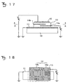
- Fig. 17 shows a cross section of an organic transistor of SIT structure of another embodiment.
- an organic semiconductor layer 13 for example of p-type, having a carrier transporting property, is so provided as to be sandwiched between a source electrode 11 and a drain electrode 15.
- the organic semiconductor layer 13 may be p-type (positive hole transporting) or n-type (electron transporting) and can be constituted of a material having at least either of the positive hole transporting property and the electron transporting property.
- a gate electrode constituted of two intermediate electrode pieces 14a, 14b each having a flat plate shape. The intermediate electrode pieces 14a, 14b are separated in mutually parallel manner between the source electrode 11 and the drain electrode 15. As shown in Fig.
- the intermediate electrode pieces 14a, 14b are mutually connected electrically as a gate electrode 14 and are so formed, when observed from the side of the source electrode 11 or the drain electrode 15, as to cover these electrodes in a mutually complementary manner.
- the intermediate electrode pieces 14a, 14b are provided in a mutually separate manner respectively in two planes between the source electrode 11 and the drain electrode 15, but intermediate electrode pieces may also be provided in three or more planes as long as they are between the source electrode 11 and the drain electrode 15.
- the organic transistor of the present embodiment is produced for example by a following process.
- a source electrode 11 is formed on a substrate 10 as shown in Fig. 19.
- a source electrode 11 of indium tin oxide (ITO) or chromium (Cr) is formed with a thickness of 50 nm by a sputtering method.
- ITO indium tin oxide
- Cr chromium
- Various methods such as evaporation, sputtering or CVD can be utilized for forming not only the source electrodes but also various electrodes.
- a film of 4,4'-bis[N-(1-naphthyl)-N-phenylamino]-biphenyl (so-called a-NPD) is formed with a thickness of 50 nm by a resistance-heated evaporation as the first organic semiconductor layer 13a.
- Al is formed in a flat plate shape with a thickness of 50 nm by a resistance-heated evaporation as the first intermediate electrode piece 14a utilizing a mask, so as to cover a part of the source electrode 11 across the first organic semiconductor layer 13a.
- a film of a-NPD same as in the first organic semiconductor layer is formed with a thickness of about 50 nm as the second organic semiconductor layer 13b.
- the entire substrate 10 is heated equal to or higher than a glass transition point of the organic semiconductor layer but equal to or less than the melting point thereof. More specifically, heating is executed at a temperature by 10 - 50° C than the glass transition temperature (96° C) of a-NPD, for example at 130° C for 10 minutes to embed the first intermediate electrode piece 14a in the second organic semiconductor layer 13b, thereby planarizing the surface thereof.
- the second organic semiconductor layer 13b is softened, and, by gravity and surface tension, fuses with the first organic semiconductor layer 13a.
- the heating process may be executed in the air, but, for the purpose of avoiding material deterioration or contamination, it is preferably executed in a vacuum chamber or in a nitrogen-replaced chamber.
- a softening temperature is about 150°C for an organic material with a glass transition temperature of 96°C, and a heating time required for softening is about 5 minutes.
- the entire substrate is heated by a heater in a reduced-pressure chamber or a vacuum chamber, and for example a halide lamp may be employed as heating means.
- Al is formed in a flat plate shape with a thickness of 50 nm by a resistance-heated evaporation as the second intermediate electrode piece 14b utilizing a mask, so as to cover another part of the source electrode 11 across the second organic semiconductor layer 13b.
- the second intermediate electrode piece 14b and the first intermediate electrode piece 14a are so formed as to cover the source electrode 11 in a mutually complementary form.
- the first intermediate electrode piece 14a and the second intermediate electrode piece 14b may be so formed, as shown in Fig. 24 as to have overlapping portions DP mutually separated across the second organic semiconductor layer 13b.
- the second intermediate electrode piece 14b is so formed as to be electrically connected with the first intermediate electrode piece 14a thereby realizing a same potential in the gate electrode 14.
- the distance between the first intermediate electrode piece 14a and the second intermediate electrode piece 14b can be made smaller than the gap between the slat-shaped branches of a prior gate electrode formed utilizing a mask in a single plane, and such pieces can be formed in a close relationship separated by the thickness of a film, with a high precision in the distance of the electrode pieces.
- a film of a-NPD same as in the first organic semiconductor layer is formed with a thickness of about 50 nm as the third organic semiconductor layer 13c.
- the entire substrate 10 is heated equal to or higher than a glass transition point of the organic semiconductor layer but equal to or less than the melting point thereof in the same manner as explained before, thereby embedding the second intermediate electrode piece 14b in the third organic semiconductor layer 13c and planarizing the surface.
- a film of Al is formed with a thickness of 200 nm as the drain electrode 15 by a resistance-heated evaporation.
- the heat treatment after the formation of the organic semiconductor layer planarizes the organic semiconductor layer thereby providing an organic transistor having uniform organic semiconductor layers without surface irregularities.
- the first, second and third organic semiconductor layers 13a, 13b, 13c are formed by a-NPD which is a p-type material, but an n-type material may also be employed.
- the organic semiconductor layer may be formed by a material having at least either of the electron transporting property and the positive hole transporting property.
- the intermediate electrode pieces 14a, 14b are formed in a flat plate shape, but it is also possible to form the intermediate electrode pieces 14a, 14b of the gate electrode 14, positioned in two planes between the source electrode 11 and the drain electrode 15, as plural slat-shaped branches in a comb-like or screen-like pattern as shown in Fig. 26. Also in such case, the intermediate electrode pieces 14a, 14b, as shown in Fig. 27, are mutually connected electrically as the gate electrode 14 and are so formed, when observed from the side of the source electrode 11 or the drain electrode 15, as to cover these electrodes in a mutually complementary manner as shown in Fig. 27.
- an electroluminescence device integral with an organic transistor can be constructed, as shown in Fig. 28, by forming the first, second and third organic semiconductor layers 13a, 13b, 13c as positive hole transport layers and providing an organic light-emitting layer 16 of an electron transporting property between the source electrode 11 and the first organic semiconductor layer 13a. It is thus rendered possible to form plural organic EL devices, each provided with an active device formed by organic material layers including an organic light-emitting layer constituted of at least a film of an organic compound showing an electroluminescence (EL) or a light emission by a current injection, in a predetermined pattern such as a matrix on a display panel substrate.
- EL electroluminescence
- An organic EL device is formed by laminating organic material layers in succession between a pair of electrode layers which are provided on a substrate and one of which at a light emitting side is constituted of a transparent material.
- the organic light emission layer 16 may be provided between the drain electrode 15 and the third organic semiconductor layer 13c in a configuration opposite to that shown in Fig. 28.
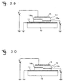
- the first intermediate electrode piece 14a and the second intermediate electrode piece 14b may be so formed as not to have portions that mutually overlap across the second organic semiconductor layer 13b.
- the intermediate electrode pieces 14a, 14b, 14c of the gate electrode are provided respectively in three planes between the source electrode 11 and the drain electrode 15.
Landscapes
- Chemical & Material Sciences (AREA)
- Engineering & Computer Science (AREA)
- Materials Engineering (AREA)
- Inorganic Chemistry (AREA)
- Physics & Mathematics (AREA)
- Spectroscopy & Molecular Physics (AREA)
- Thin Film Transistor (AREA)
- Junction Field-Effect Transistors (AREA)
Abstract
The invention provides an organic semiconductor device with
a p-type organic semiconductor layer sandwiched between a source
electrode and a drain electrode including an n-type organic
semiconductor layer formed in an intermediate portion of the p-type
organic semiconductor layer and a gate electrode embedded in the
n-type organic semiconductor layer, and an organic semiconductor
device with an n-type organic semiconductor layer sandwiched
between a source electrode and a drain electrode includes a p-type
organic semiconductor layer formed in an intermediate portion
of the n-type organic semiconductor layer and a gate electrode
embedded in the p-type organic semiconductor layer, thereby
suppressing a leak current generated between the electrodes. The
invention also provides an organic semiconductor device including
an organic semiconductor layer sandwiched between a source
electrode and a drain electrode and having a carrier transporting
property, and a gate electrode constituted of at least two
intermediate electrode pieces which are embedded in the organic
semiconductor layer, are respectively provided in at least two
planes separated from and parallel to the source electrode and
the drain electrode, and are positioned in a direction across
the layer thickness. The gate electrode is embedded by fusing
the organic semiconductor layer.
Description
The present invention relates to an organic semiconductor
device provided with an organic semiconductor layer constituted
of an organic compound having a carrier transporting property,
and a producing method therefor.
As a voltage application to an organic semiconductor layer
causes a charge density increase therein, a current can be induced
between a pair of electrodes provided on such organic semiconductor
layer. For example, in an organic semiconductor device such as
an organic transistor of a vertical SIT (static induction
transistor) structure, a gate electrode, positioned between a
source electrode and a drain electrode sandwiching an organic
semiconductor layer, applies a voltage across the thickness of
such organic semiconductor layer to switch a current in a direction
of thickness of the organic semiconductor layer.
An SIT, as shown in Fig. 1, has a three-terminal structure
in which an organic semiconductor layer 13 is sandwiched between
a pair of a source electrode 11 and a drain electrode 15 and a
gate electrode 14 is formed within the thickness of the organic
semiconductor layer. A voltage is applied to the gate electrode,
and a current between the source electrode and the drain electrode
can be controlled by a depletion layer DpL generated in the organic
semiconductor layer.
In the organic transistor of SIT structure, a carrier
displacement across the film thickness between the source
electrode and the drain electrode is prevented by plural depletion
layers DpL formed in the organic semiconductor layer around plural
slat-shaped branches of the gate electrode 14 receiving for example
a positive charge.
However, in case each depletion layer DpL has an insufficient
spreading, a gap W between the slat-shaped branches of the gate
electrode 14 as shown in Fig. 2 cannot be filled with the depletion
layer DpL, thereby resulting in an increase in a leak current.
Thus, the gate electrode has to be formed with a fine-structured
mask in order to reduce the gap between the slat-shaped branches
of the gate electrode, thereby preventing the carrier displacement
and decreasing the leak current.
In general, in an organic transistor of an SIT structure,
the organic semiconductor layer has a thickness in the order of
several hundred nanometers and the gate electrode formed between
the source electrode and the drain electrode has a thickness of
50 to 100 nm. Thus, in case of forming the organic semiconductor
layer, the gate electrode and the organic semiconductor layer
by successive film formations in the organic transistor, the shape
of the plural slat-shaped branches of the gate electrode is
transferred onto the organic semiconductor layer and the drain
electrode to be deposited in ensuing steps, thereby forming
irregularities on the surface and inducing an increase in the
leak current.
A problem to be solved by the present invention is to provide
an organic semiconductor device capable suppressing generation
of a leak current between the electrodes.
The present invention provides an organic semiconductor
device comprising: a source electrode; a drain electrode; and
a p-type organic semiconductor layer sandwiched between the source
electrode and the drain electrode, characterized by further
comprising an n-type organic semiconductor layer formed in an
intermediate portion of the p-type organic semiconductor layer;
and a gate electrode embedded in the n-type organic semiconductor
layer.
The present invention also provides an organic
semiconductor device comprising: a source electrode; a drain
electrode; and a n-type organic semiconductor layer sandwiched
between the source electrode and the drain electrode,
characterized by further comprising a p-type organic
semiconductor layer formed in an intermediate portion of said
n-type organic semiconductor layer and a gate electrode embedded
in said p-type organic semiconductor layer.
The present invention also provides an organic
semiconductor device comprising: a source electrode; a drain
electrode; and an organic semiconductor layer sandwiched between
the source electrode and the drain electrode and having a carrier
transporting property, characterized by further comprising a gate
electrode constituted of at least two intermediate electrode
pieces which are embedded in the organic semiconductor layer,
wherein the intermediate electrode pieces are respectively
provided in at least two planes separated from and parallel to
the source electrode and the drain electrode, and are positioned
in a direction across the layer thickness.
The present invention also provides a method for producing
an organic semiconductor device provided with an organic
semiconductor layer formed between a source electrode and a drain
electrode and embedding a gate electrode therein, the method
characterized by comprising:
As an embodiment of the organic semiconductor device of
the present invention, an organic transistor will be explained
with reference to the accompanying drawings.
Fig. 3 illustrates a cross section of an organic transistor
of an SIT structure in an embodiment. In the organic transistor,
on a source electrode formed on a substrate 10, there are laminated
in succession a first p-type organic semiconductor layer 13p1,
a first n-type organic semiconductor layer 13n1, a gate electrode
14, a second n-type organic semiconductor layer 13n2, a second
p-type organic semiconductor layer 13p2, and a drain electrode
15. These organic semiconductor layers have a carrier
transporting property, and the first p-type organic semiconductor
layer 13p1 and the second p-type organic semiconductor layer 13p2
are formed by a p-type organic semiconductor material (positive
hole transporting), while the first n-type organic semiconductor
layer 13n1 and the second n-type organic semiconductor layer 13n2
are formed by an n-type organic semiconductor material (electron
transporting). Such device includes a pnp junction, of which
areas are respectively connected to a source electrode 11, a gate
electrode 14 and a drain electrode 15. Therefore, the organic
transistor of the present embodiment in its entire configuration
constitutes an organic semiconductor device having a p-type
organic semiconductor layer sandwiched between the source
electrode 11 and the drain electrode 15, and a carrier displacement
is controlled by the n-type organic semiconductor layer (first
n-type organic semiconductor layer 13n1 and second n-type organic
semiconductor layer 13n2) positioned between the p-type organic
semiconductor layers (first p-type organic semiconductor layer
13p1 and second p-type organic semiconductor layer 13p2). In
order to apply a control voltage uniformly to such n-type organic
semiconductor layer, the gate electrode 14 is embedded in the
n-type organic semiconductor layer.
As shown in Fig. 4, the gate electrode 14 is so formed,
when observed from the side of the source electrode 11 or the
drain electrode 15, as to cover these electrodes.
The organic transistor of the present embodiment is produced
for example by a following process.
At first, a source electrode 11 is formed on a substrate
10 as shown in Fig. 5. For example a source electrode 11 of indium
tin oxide (ITO) or chromium (Cr) is formed with a thickness of
50 nm by a sputtering method. Various methods such as evaporation,
sputtering or CVD can be utilized for forming not only the source
electrodes but also various electrodes.
Then, as shown in Fig. 6, on the source electrode 11, a
film of 4,4'-bis[N-(1-naphthyl)-N-phenylamino]-biphenyl
(so-called a-NPD) is formed with a thickness of 25 nm by a
resistance-heated evaporation as the first p-type organic
semiconductor layer 13p1.
Then, as shown in Fig. 7, on the first p-type organic
semiconductor film 13p1, a film of a porphyrin compound such as
copper phthalocyanine (so-called CuPc) or a quinoline derivative
such as tris(8-hydroxyquinoline) aluminum complex (so-called
Alq3) is formed with a thickness of 25 nm by a resistance-heated
evaporation as the first n-type organic semiconductor layer 13n1.
Then, as shown in Fig. 8, aluminum is formed in a flat plate
shape with a thickness of 50 nm as the gate electrode 14 by a
resistance-heated evaporation. Also the entire gate electrode
14 may be covered for example with an electron injection layer
of a thickness of several nanometers such as of LiO2.
Then, as shown in Fig. 9, on the gate electrode 14, a film
of CuPc or Alq3 same as in the first n-type organic semiconductor
layer is formed with a thickness of 25 nm as the second n-type
organic semiconductor layer 13n2 by a resistance-heated
evaporation.
Then, as shown in Fig. 10, on the second n-type organic
semiconductor layer 13n2, a film of a-NPD same as in the first
p-type organic semiconductor layer is formed with a thickness
of 25 nm as the second p-type organic semiconductor layer 13p2.
Finally, as shown in Fig. 11, on the second p-type organic
semiconductor layer 13p2, a film of Al is formed with a thickness
of 200 nm as the drain electrode 15 by a resistance-heated
evaporation, thereby completing an organic transistor.
In the obtained organic transistor, for example in a state
where the drain electrode 15 is grounded and the source electrode
11 is maintained at a potential of +10 V as shown in Fig. 12,
a potential of +20 V applied to the gate electrode 14 elevates
the barrier thereby turning off the transistor. On the other
hand, in a same state where the drain electrode 15 is grounded
and the source electrode 11 is maintained at a potential of +10
V, an open state of the gate electrode 14 as shown in Fig. 13
merely leaves junctions of the organic semiconductor layers
whereby the transistor is turned on to permit a current
therethrough.
The foregoing embodiment has shown an example of a pnp
junction, but an npn junction may also be adopted. In such case,
the device is constituted, on a source electrode on a substrate
10 as shown in Fig. 14, of a first n-type organic semiconductor
layer 13n1, a first p-type organic semiconductor layer 13p1, a
gate electrode 14, a second p-type organic semiconductor layer
13p2, a second n-type organic semiconductor layer 13n2 and a drain
electrode 15 laminated in succession. Therefore, the organic
transistor can also be so constructed as to include a p-type organic
semiconductor layer, constituted of the first p-type organic
semiconductor layer 13p1 and the second p-type organic
semiconductor layer 13p2, and sandwiched in the n-type organic
semiconductor layer constituted of the first and second n-type
organic semiconductor layers 13n1, 13n2 which are positioned
between the source electrode 11 and the drain electrode 15, and
also the gate electrode 14 embedded in the first p-type organic
semiconductor layer 13p1 and the second p-type organic
semiconductor layer 13p2.
Also in the foregoing embodiment, the gate electrode 14
is formed as flat plate shape, but the gate electrode 14 may also
be formed, as shown in Fig. 15, as plural slat-shaped branches
in a comb-like or screen-like pattern. In such case, the gate
electrode may be formed in any shape that can apply a voltage
substantially uniformly to the contacting organic semiconductor
layer.
Furthermore, in the organic transistor of the
aforementioned SIT structure, an electroluminescence device
integral with an organic transistor can be constructed, as shown
in Fig. 16, by forming the first p-type organic semiconductor
layer 13p1 and the second p-type organic semiconductor layer 13p2
as positive hole transport layers and providing an organic
light-emitting layer 16 of an electron transporting property
between the source electrode 11 and the first p-type organic
semiconductor layer 13p1. It is thus rendered possible to form
plural organic EL devices, each provided with an active device
formed by organic material layers including an organic
light-emitting layer constituted of at least a film of an organic
compound showing an electroluminescence (EL) or a light emission
by a current injection, in a predetermined pattern such as a matrix
on a display panel substrate.
An organic EL device is formed by laminating organic material
layers in succession between a pair of electrode layers which
are provided on a substrate and one of which at a light emitting
side is constituted of a transparent material. For example in
a top-emission configuration, the organic light emission layer
16 may be provided between the drain electrode 15 and the second
p-type organic semiconductor layer 13p2 in a configuration
opposite to that shown in Fig. 16.
Fig. 17 shows a cross section of an organic transistor of
SIT structure of another embodiment. On a substrate 10, an organic
semiconductor layer 13 for example of p-type, having a carrier
transporting property, is so provided as to be sandwiched between
a source electrode 11 and a drain electrode 15. The organic
semiconductor layer 13 may be p-type (positive hole transporting)
or n-type (electron transporting) and can be constituted of a
material having at least either of the positive hole transporting
property and the electron transporting property. In the organic
semiconductor layer 13, there is embedded a gate electrode
constituted of two intermediate electrode pieces 14a, 14b each
having a flat plate shape. The intermediate electrode pieces
14a, 14b are separated in mutually parallel manner between the
source electrode 11 and the drain electrode 15. As shown in Fig.
18, the intermediate electrode pieces 14a, 14b are mutually
connected electrically as a gate electrode 14 and are so formed,
when observed from the side of the source electrode 11 or the
drain electrode 15, as to cover these electrodes in a mutually
complementary manner. The intermediate electrode pieces 14a,
14b are provided in a mutually separate manner respectively in
two planes between the source electrode 11 and the drain electrode
15, but intermediate electrode pieces may also be provided in
three or more planes as long as they are between the source electrode
11 and the drain electrode 15.
The organic transistor of the present embodiment is produced
for example by a following process.
At first, a source electrode 11 is formed on a substrate
10 as shown in Fig. 19. For example a source electrode 11 of
indium tin oxide (ITO) or chromium (Cr) is formed with a thickness
of 50 nm by a sputtering method. Various methods such as
evaporation, sputtering or CVD can be utilized for forming not
only the source electrodes but also various electrodes.
Then, as shown in Fig. 20, on the source electrode 11, a
film of 4,4'-bis[N-(1-naphthyl)-N-phenylamino]-biphenyl
(so-called a-NPD) is formed with a thickness of 50 nm by a
resistance-heated evaporation as the first organic semiconductor
layer 13a.
Then, as shown in Fig. 21, on a part of an upper surface
of the first organic semiconductor layer 13a, Al is formed in
a flat plate shape with a thickness of 50 nm by a resistance-heated
evaporation as the first intermediate electrode piece 14a
utilizing a mask, so as to cover a part of the source electrode
11 across the first organic semiconductor layer 13a.
Then, as shown in Fig. 22, on the other part of the first
organic semiconductor layer 13a and the first intermediate
electrode piece 14a, a film of a-NPD same as in the first organic
semiconductor layer is formed with a thickness of about 50 nm
as the second organic semiconductor layer 13b. Then the entire
substrate 10 is heated equal to or higher than a glass transition
point of the organic semiconductor layer but equal to or less
than the melting point thereof. More specifically, heating is
executed at a temperature by 10 - 50° C than the glass transition
temperature (96° C) of a-NPD, for example at 130° C for 10 minutes
to embed the first intermediate electrode piece 14a in the second
organic semiconductor layer 13b, thereby planarizing the surface
thereof. The second organic semiconductor layer 13b is softened,
and, by gravity and surface tension, fuses with the first organic
semiconductor layer 13a. The heating process may be executed
in the air, but, for the purpose of avoiding material deterioration
or contamination, it is preferably executed in a vacuum chamber
or in a nitrogen-replaced chamber. A softening temperature is
about 150°C for an organic material with a glass transition
temperature of 96°C, and a heating time required for softening
is about 5 minutes. The entire substrate is heated by a heater
in a reduced-pressure chamber or a vacuum chamber, and for example
a halide lamp may be employed as heating means.
Then, as shown in Fig. 23, on a part of an upper surface
of the second organic semiconductor layer 13b, Al is formed in
a flat plate shape with a thickness of 50 nm by a resistance-heated
evaporation as the second intermediate electrode piece 14b
utilizing a mask, so as to cover another part of the source electrode
11 across the second organic semiconductor layer 13b. The second
intermediate electrode piece 14b and the first intermediate
electrode piece 14a are so formed as to cover the source electrode
11 in a mutually complementary form. The first intermediate
electrode piece 14a and the second intermediate electrode piece
14b may be so formed, as shown in Fig. 24 as to have overlapping
portions DP mutually separated across the second organic
semiconductor layer 13b. The second intermediate electrode piece
14b is so formed as to be electrically connected with the first
intermediate electrode piece 14a thereby realizing a same
potential in the gate electrode 14. By such film formation of
the second organic semiconductor layer 13b, the distance between
the first intermediate electrode piece 14a and the second
intermediate electrode piece 14b can be made smaller than the
gap between the slat-shaped branches of a prior gate electrode
formed utilizing a mask in a single plane, and such pieces can
be formed in a close relationship separated by the thickness of
a film, with a high precision in the distance of the electrode
pieces.
Then, as shown in Fig. 24, on the other part of the second
organic semiconductor layer 13b and the second intermediate
electrode piece 14b, a film of a-NPD same as in the first organic
semiconductor layer is formed with a thickness of about 50 nm
as the third organic semiconductor layer 13c. Then the entire
substrate 10 is heated equal to or higher than a glass transition
point of the organic semiconductor layer but equal to or less
than the melting point thereof in the same manner as explained
before, thereby embedding the second intermediate electrode piece
14b in the third organic semiconductor layer 13c and planarizing
the surface.
Finally, as shown in Fig. 25, on the third organic
semiconductor layer 13c, a film of Al is formed with a thickness
of 200 nm as the drain electrode 15 by a resistance-heated
evaporation. The heat treatment after the formation of the
organic semiconductor layer planarizes the organic semiconductor
layer thereby providing an organic transistor having uniform
organic semiconductor layers without surface irregularities.
In the foregoing embodiment, the first, second and third
organic semiconductor layers 13a, 13b, 13c are formed by a-NPD
which is a p-type material, but an n-type material may also be
employed. The organic semiconductor layer may be formed by a
material having at least either of the electron transporting
property and the positive hole transporting property.
Also in the foregoing embodiment, the intermediate
electrode pieces 14a, 14b are formed in a flat plate shape, but
it is also possible to form the intermediate electrode pieces
14a, 14b of the gate electrode 14, positioned in two planes between
the source electrode 11 and the drain electrode 15, as plural
slat-shaped branches in a comb-like or screen-like pattern as
shown in Fig. 26. Also in such case, the intermediate electrode
pieces 14a, 14b, as shown in Fig. 27, are mutually connected
electrically as the gate electrode 14 and are so formed, when
observed from the side of the source electrode 11 or the drain
electrode 15, as to cover these electrodes in a mutually
complementary manner as shown in Fig. 27.
Furthermore, in the organic transistor of the
aforementioned SIT structure, an electroluminescence device
integral with an organic transistor can be constructed, as shown
in Fig. 28, by forming the first, second and third organic
semiconductor layers 13a, 13b, 13c as positive hole transport
layers and providing an organic light-emitting layer 16 of an
electron transporting property between the source electrode 11
and the first organic semiconductor layer 13a. It is thus rendered
possible to form plural organic EL devices, each provided with
an active device formed by organic material layers including an
organic light-emitting layer constituted of at least a film of
an organic compound showing an electroluminescence (EL) or a light
emission by a current injection, in a predetermined pattern such
as a matrix on a display panel substrate.
An organic EL device is formed by laminating organic material
layers in succession between a pair of electrode layers which
are provided on a substrate and one of which at a light emitting
side is constituted of a transparent material. For example in
a top-emission configuration, the organic light emission layer
16 may be provided between the drain electrode 15 and the third
organic semiconductor layer 13c in a configuration opposite to
that shown in Fig. 28.
In another embodiment of the organic transistor of the
invention, as shown in Figs. 29 and 30, the first intermediate
electrode piece 14a and the second intermediate electrode piece
14b may be so formed as not to have portions that mutually overlap
across the second organic semiconductor layer 13b.
Also in another embodiment of the organic transistor of
the invention, as shown in Fig. 31, the intermediate electrode
pieces 14a, 14b, 14c of the gate electrode, each formed as plural
slat-shaped branches of a comb-shaped or screen-like pattern,
are provided respectively in three planes between the source
electrode 11 and the drain electrode 15.
Claims (14)
- An organic semiconductor device comprising: a source electrode; a drain electrode; and a p-type organic semiconductor layer sandwiched between the source electrode and the drain electrode, characterized by further comprising an n-type organic semiconductor layer formed in an intermediate portion of the p-type organic semiconductor layer; and a gate electrode embedded in the n-type organic semiconductor layer.
- An organic semiconductor device according to claim 1, characterized in that the gate electrode has a flat plate shape.
- An organic semiconductor device according to claim 1, characterized in that the gate electrode is formed in a comb-like or screen-like pattern.
- An organic semiconductor device comprising: a source electrode; a drain electrode; and a n-type organic semiconductor layer sandwiched between the source electrode and the drain electrode, characterized by further comprising a p-type organic semiconductor layer formed in an intermediate portion of said n-type organic semiconductor layer and a gate electrode embedded in said p-type organic semiconductor layer.
- An organic semiconductor device according to claim 4, characterized in that the gate electrode has a flat plate shape.
- An organic semiconductor device according to claim 4, characterized in that the gate electrode is formed in a comb-like or screen-like pattern.
- An organic semiconductor device comprising: a source electrode; a drain electrode; and an organic semiconductor layer sandwiched between the source electrode and the drain electrode and having a carrier transporting property, characterized by further comprising a gate electrode constituted of at least two intermediate electrode pieces which are embedded in the organic semiconductor layer, wherein the intermediate electrode pieces are respectively provided in at least two planes separated from and parallel to the source electrode and the drain electrode, and are positioned in a direction across the layer thickness.
- An organic semiconductor device according to claim 7, characterized in that the intermediate electrode piece has a flat plate shape.
- An organic semiconductor device according to claim 7, characterized in that the intermediate electrode piece is formed in a comb-like or screen-like pattern.
- An organic semiconductor device according to any of claims 7 to 9, characterized in that the organic semiconductor layer is constituted of a material having at least either of an electron transporting property and a positive hole transporting property.
- An organic semiconductor device according to any of claims 7 to 9, characterized in that the two intermediate electrode pieces have overlapping portions which are mutually separated across a part of the organic semiconductor layer.
- A method for producing an organic semiconductor device provided with an organic semiconductor layer formed between a source electrode and a drain electrode and embedding a gate electrode therein, the method being characterized by comprising:a first organic semiconductor layer laminating step of forming a first organic semiconductor layer on either of a source electrode and a drain electrode;a first intermediate electrode piece laminating step of forming a first intermediate electrode piece on a part of the first organic semiconductor layer;a second organic semiconductor layer laminating step of forming a second organic semiconductor layer on the first organic semiconductor layer and the first intermediate electrode piece;a second intermediate electrode piece laminating step of forming a second intermediate electrode piece on a part of the second organic semiconductor layer so as to cover the source electrode and the drain electrode in a complementary manner with the first intermediate electrode piece; anda third organic semiconductor layer laminating step of forming a third organic semiconductor layer on the second organic semiconductor layer and the second intermediate electrode piece;wherein each of the second and third organic semiconductor layer laminating step includes an embedding step of softening the formed organic semiconductor and embedding the intermediate electrode piece therein.
- A method for producing an organic semiconductor device according to claim 12, characterized in that the embedding step heats the first organic semiconductor layer to a temperature equal to or higher than a glass transition temperature thereof but equal to or lower than a melting point thereof.
- A method for producing an organic semiconductor device according to claim 12, characterized in that the organic semiconductor layer is formed by an evaporation method.
Applications Claiming Priority (5)
| Application Number | Priority Date | Filing Date | Title |
|---|---|---|---|
| JP2002205635 | 2002-07-15 | ||
| JP2002205634A JP2004047881A (en) | 2002-07-15 | 2002-07-15 | Organic semiconductor device and method of manufacturing the same |
| JP2002205635A JP4331921B2 (en) | 2002-07-15 | 2002-07-15 | Organic semiconductor device |
| JP2002205634 | 2002-07-15 | ||
| PCT/JP2003/008761 WO2004008545A1 (en) | 2002-07-15 | 2003-07-10 | Organic semiconductor device and method for manufacturing same |
Publications (2)
| Publication Number | Publication Date |
|---|---|
| EP1536484A1 true EP1536484A1 (en) | 2005-06-01 |
| EP1536484A4 EP1536484A4 (en) | 2009-01-07 |
Family
ID=30117464
Family Applications (1)
| Application Number | Title | Priority Date | Filing Date |
|---|---|---|---|
| EP03741311A Withdrawn EP1536484A4 (en) | 2002-07-15 | 2003-07-10 | ORGANIC SEMICONDUCTOR AND METHOD FOR MANUFACTURING THE SAME |
Country Status (6)
| Country | Link |
|---|---|
| US (1) | US20060208251A1 (en) |
| EP (1) | EP1536484A4 (en) |
| KR (1) | KR20050028020A (en) |
| CN (1) | CN1669156A (en) |
| AU (1) | AU2003281009A1 (en) |
| WO (1) | WO2004008545A1 (en) |
Families Citing this family (17)
| Publication number | Priority date | Publication date | Assignee | Title |
|---|---|---|---|---|
| US7554121B2 (en) * | 2003-12-26 | 2009-06-30 | Semiconductor Energy Laboratory Co., Ltd. | Organic semiconductor device |
| US7659138B2 (en) * | 2003-12-26 | 2010-02-09 | Semiconductor Energy Laboratory Co., Ltd. | Method for manufacturing an organic semiconductor element |
| GB0400997D0 (en) * | 2004-01-16 | 2004-02-18 | Univ Cambridge Tech | N-channel transistor |
| CN100569036C (en) * | 2004-02-16 | 2009-12-09 | 独立行政法人科学技术振兴机构 | Light emitting transistor and laser light source |
| CN100487930C (en) * | 2004-08-30 | 2009-05-13 | 国立大学法人京都大学 | Organic semiconductor light emitting device and display device using the same |
| WO2006046521A1 (en) * | 2004-10-25 | 2006-05-04 | Matsushita Electric Industrial Co., Ltd. | Electronic device, process for producing the same and electronic equipment making use thereof |
| KR20060080446A (en) * | 2005-01-05 | 2006-07-10 | 삼성전자주식회사 | Vertical organic thin film transistor and organic light emitting transistor |
| US20090140955A1 (en) * | 2005-10-14 | 2009-06-04 | Pioneer Corporation | Light-emitting element and display device |
| KR100741102B1 (en) * | 2005-12-22 | 2007-07-20 | 삼성에스디아이 주식회사 | Method for manufacturing organic thin film transistor, organic thin film transistor, and flat panel display device having same |
| KR100794570B1 (en) * | 2006-04-06 | 2008-01-17 | 서강대학교산학협력단 | Vertical organic thin film transistor and manufacturing method thereof |
| KR20090002787A (en) * | 2007-07-04 | 2009-01-09 | 삼성전자주식회사 | Light emitting device and light receiving device using transistor structure |
| JP5347377B2 (en) * | 2007-08-31 | 2013-11-20 | 大日本印刷株式会社 | Vertical organic transistor, manufacturing method thereof, and light emitting device |
| FR2953994B1 (en) * | 2009-12-15 | 2012-06-08 | Commissariat Energie Atomique | SOURCE OF PHOTONS RESULTING FROM A RECOMBINATION OF LOCALIZED EXCITONS |
| DE102010041331A1 (en) * | 2010-09-24 | 2012-03-29 | Siemens Aktiengesellschaft | Charge carrier modulation for color and brightness tuning in organic light-emitting diodes |
| CN104335379B (en) * | 2012-05-31 | 2016-12-21 | 乐金显示有限公司 | Organic electroluminescence device, the display comprising this organic electroluminescence device and luminaire |
| JP6116018B2 (en) | 2015-01-29 | 2017-04-19 | 国立大学法人 東京大学 | Organic semiconductor device |
| US11049948B2 (en) * | 2018-06-29 | 2021-06-29 | Solsona Enterprise, Llc | Vertical thin film transistor with perforated or comb-gate electrode configuration |
Family Cites Families (14)
| Publication number | Priority date | Publication date | Assignee | Title |
|---|---|---|---|---|
| GB2169608B (en) * | 1984-12-28 | 1988-02-24 | Hoechst Gosei Kk | Process for producting electrically conductive composite polymer article |
| JPS6419778A (en) * | 1987-07-15 | 1989-01-23 | Fuji Electric Co Ltd | Electrostatic induction type field-effect transistor |
| JPH01209767A (en) * | 1988-02-18 | 1989-08-23 | Canon Inc | Electric/electronic device element |
| DE19534494A1 (en) * | 1995-09-18 | 1997-03-20 | Basf Ag | Transistor useful as electronic switch, amplifier, diode, LED or chemical sensor |
| JP3268993B2 (en) * | 1997-01-31 | 2002-03-25 | 三洋電機株式会社 | Display device |
| US5917280A (en) * | 1997-02-03 | 1999-06-29 | The Trustees Of Princeton University | Stacked organic light emitting devices |
| US6337492B1 (en) * | 1997-07-11 | 2002-01-08 | Emagin Corporation | Serially-connected organic light emitting diode stack having conductors sandwiching each light emitting layer |
| US6420031B1 (en) * | 1997-11-03 | 2002-07-16 | The Trustees Of Princeton University | Highly transparent non-metallic cathodes |
| JP3403136B2 (en) * | 1999-12-28 | 2003-05-06 | 株式会社東芝 | Method for manufacturing switching element, switching element and switching element array |
| AU2001281343A1 (en) * | 2000-07-24 | 2002-02-05 | Northwestern University | N-type thiophene semiconductors |
| US6884093B2 (en) * | 2000-10-03 | 2005-04-26 | The Trustees Of Princeton University | Organic triodes with novel grid structures and method of production |
| DE10051369A1 (en) * | 2000-10-17 | 2002-05-02 | Fraunhofer Ges Forschung | Polymer switching element |
| JP3856202B2 (en) * | 2001-10-05 | 2006-12-13 | 日本電気株式会社 | Organic thin film transistor |
| EP1367659B1 (en) * | 2002-05-21 | 2012-09-05 | Semiconductor Energy Laboratory Co., Ltd. | Organic field effect transistor |
-
2003
- 2003-07-10 KR KR1020057000613A patent/KR20050028020A/en not_active Ceased
- 2003-07-10 WO PCT/JP2003/008761 patent/WO2004008545A1/en not_active Ceased
- 2003-07-10 AU AU2003281009A patent/AU2003281009A1/en not_active Abandoned
- 2003-07-10 CN CNA03816762XA patent/CN1669156A/en active Pending
- 2003-07-10 EP EP03741311A patent/EP1536484A4/en not_active Withdrawn
- 2003-07-10 US US10/521,442 patent/US20060208251A1/en not_active Abandoned
Also Published As
| Publication number | Publication date |
|---|---|
| US20060208251A1 (en) | 2006-09-21 |
| CN1669156A (en) | 2005-09-14 |
| EP1536484A4 (en) | 2009-01-07 |
| KR20050028020A (en) | 2005-03-21 |
| AU2003281009A1 (en) | 2004-02-02 |
| WO2004008545A1 (en) | 2004-01-22 |
Similar Documents
| Publication | Publication Date | Title |
|---|---|---|
| EP1536484A1 (en) | Organic semiconductor device and method for manufacturing same | |
| TW589919B (en) | Method for vapor deposition and method for making display device | |
| TWI362229B (en) | Organic light-emitting transistor and display device | |
| KR101074806B1 (en) | Organic light emitting diode display apparatus and Method thereof | |
| US7492096B2 (en) | Flat panel display device capable of reducing or preventing a voltage drop and method of fabricating the same | |
| US20140285914A1 (en) | Method for manufacturing display device and display device | |
| JP2005005149A (en) | Organic EL device and manufacturing method thereof | |
| US9502684B2 (en) | Organic electroluminescence device and method for manufacturing the same | |
| CN102544386A (en) | Organic light emitting display device and manufacturing method for the same | |
| KR20000058036A (en) | Organic el device and method for manufacturing same | |
| WO2003069960A1 (en) | Organic semiconductor device and method for manufacturing the same | |
| KR20140055634A (en) | Organic electroluminescence display panel and manufacturing method thereof | |
| US20090135105A1 (en) | Light-emitting element and display apparatus using the same | |
| JP2000091067A (en) | Organic electroluminescence device and method of manufacturing the same | |
| TW200305119A (en) | Electroluminescence display device and method for making the same | |
| KR20150075353A (en) | Display device | |
| CN100469201C (en) | Display device and manufacturing method thereof | |
| US7586255B2 (en) | Organic electro-luminescent display of dual-panel type and method for manufacturing the same | |
| JP2003258267A (en) | Organic thin film semiconductor element and its manufacturing method | |
| KR102037487B1 (en) | Method for fabricating Organic Electroluminescence Device and the Organic Electroluminescence Device fabricated by the method | |
| CN110429185B (en) | Electroluminescent device and manufacturing method and application thereof | |
| JP2004047881A (en) | Organic semiconductor device and method of manufacturing the same | |
| JP4331921B2 (en) | Organic semiconductor device | |
| CN104992961A (en) | Organic electroluminescent transistor array substrate and manufacturing method thereof, and display device | |
| US7842943B2 (en) | Organic thin film transistor and flat panel display device using the same |
Legal Events
| Date | Code | Title | Description |
|---|---|---|---|
| PUAI | Public reference made under article 153(3) epc to a published international application that has entered the european phase |
Free format text: ORIGINAL CODE: 0009012 |
|
| 17P | Request for examination filed |
Effective date: 20050114 |
|
| AK | Designated contracting states |
Kind code of ref document: A1 Designated state(s): AT BE BG CH CY CZ DE DK EE ES FI FR GB GR HU IE IT LI LU MC NL PT RO SE SI SK TR |
|
| AX | Request for extension of the european patent |
Extension state: AL LT LV MK |
|
| DAX | Request for extension of the european patent (deleted) | ||
| RBV | Designated contracting states (corrected) |
Designated state(s): DE FR GB |
|
| A4 | Supplementary search report drawn up and despatched |
Effective date: 20081204 |
|
| STAA | Information on the status of an ep patent application or granted ep patent |
Free format text: STATUS: THE APPLICATION HAS BEEN WITHDRAWN |
|
| 18W | Application withdrawn |
Effective date: 20090105 |