EP1536473B1 - Organische elektrolumineszente Anzeigevorrichtung und Herstellungsverfahren - Google Patents
Organische elektrolumineszente Anzeigevorrichtung und Herstellungsverfahren Download PDFInfo
- Publication number
- EP1536473B1 EP1536473B1 EP04090474A EP04090474A EP1536473B1 EP 1536473 B1 EP1536473 B1 EP 1536473B1 EP 04090474 A EP04090474 A EP 04090474A EP 04090474 A EP04090474 A EP 04090474A EP 1536473 B1 EP1536473 B1 EP 1536473B1
- Authority
- EP
- European Patent Office
- Prior art keywords
- curvature
- radius
- electrode
- corners
- center
- Prior art date
- Legal status (The legal status is an assumption and is not a legal conclusion. Google has not performed a legal analysis and makes no representation as to the accuracy of the status listed.)
- Expired - Lifetime
Links
Images








Classifications
-
- H—ELECTRICITY
- H05—ELECTRIC TECHNIQUES NOT OTHERWISE PROVIDED FOR
- H05B—ELECTRIC HEATING; ELECTRIC LIGHT SOURCES NOT OTHERWISE PROVIDED FOR; CIRCUIT ARRANGEMENTS FOR ELECTRIC LIGHT SOURCES, IN GENERAL
- H05B33/00—Electroluminescent light sources
- H05B33/12—Light sources with substantially two-dimensional [2D] radiating surfaces
- H05B33/26—Light sources with substantially two-dimensional [2D] radiating surfaces characterised by the composition or arrangement of the conductive material used as an electrode
-
- H—ELECTRICITY
- H10—SEMICONDUCTOR DEVICES; ELECTRIC SOLID-STATE DEVICES NOT OTHERWISE PROVIDED FOR
- H10K—ORGANIC ELECTRIC SOLID-STATE DEVICES
- H10K77/00—Constructional details of devices covered by this subclass and not covered by groups H10K10/80, H10K30/80, H10K50/80 or H10K59/80
- H10K77/10—Substrates, e.g. flexible substrates
- H10K77/111—Flexible substrates
-
- H—ELECTRICITY
- H10—SEMICONDUCTOR DEVICES; ELECTRIC SOLID-STATE DEVICES NOT OTHERWISE PROVIDED FOR
- H10K—ORGANIC ELECTRIC SOLID-STATE DEVICES
- H10K50/00—Organic light-emitting devices
- H10K50/80—Constructional details
- H10K50/805—Electrodes
- H10K50/81—Anodes
- H10K50/813—Anodes characterised by their shape
-
- H—ELECTRICITY
- H10—SEMICONDUCTOR DEVICES; ELECTRIC SOLID-STATE DEVICES NOT OTHERWISE PROVIDED FOR
- H10K—ORGANIC ELECTRIC SOLID-STATE DEVICES
- H10K59/00—Integrated devices, or assemblies of multiple devices, comprising at least one organic light-emitting element covered by group H10K50/00
- H10K59/80—Constructional details
- H10K59/805—Electrodes
- H10K59/8051—Anodes
- H10K59/80515—Anodes characterised by their shape
-
- H—ELECTRICITY
- H10—SEMICONDUCTOR DEVICES; ELECTRIC SOLID-STATE DEVICES NOT OTHERWISE PROVIDED FOR
- H10K—ORGANIC ELECTRIC SOLID-STATE DEVICES
- H10K59/00—Integrated devices, or assemblies of multiple devices, comprising at least one organic light-emitting element covered by group H10K50/00
- H10K59/10—OLED displays
- H10K59/12—Active-matrix OLED [AMOLED] displays
Definitions
- the present invention relates to an organic electroluminescent display device and method for manufacturing the same. More particularly, the invention is directed to an organic electroluminescent display device and method for fabricating the same, in which corners of a lower (pixel) electrode are rounded off, thereby preventing contamination caused by outgassing and short-induced defects.
- AMOLED active matrix organic light emitting devices
- OELDs organic electroluminescence devices
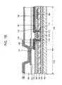
- FIG. 1A shows a planar structure of a conventional AMOLED having two transistors and a capacitor.
- FIG. 1B is a cross-sectional view taken along the line I-I of FIG. 1A .
- the conventional AMOLED includes an emission region 110 and a non emission region 130.
- a lower electrode 131 e.g., a pixel electrode
- an organic emission layer 132 and an upper electrode 133 are formed in the emission region 110 .
- two thin film transistors (TFTs) and a capacitor are formed in the non-emission region 130.
- a buffer layer 140 is formed on a transparent insulating substrate 100 such as a glass substrate, and an amorphous silicon layer is deposited on the buffer layer to form a semiconductor layer 111.
- the semiconductor layer 111 is formed by performing a crystallization process after patterning the deposited amorphous silicon layer.
- a gate insulating layer 150 is formed on the entire surface of the substrate.
- a metallic material for a gate electrode is deposited and patterned on the gate insulating layer 150 to form a gate 112 on the semiconductor layer 111.
- a capacitor lower electrode 122 is simultaneously formed at this time.
- a gate line 102 of FIG. 1A is also formed.
- source/drain regions 113 and 114 are formed by ion implantation of, for example, P or N type impurities, into the semiconductor layer 111.
- an interlayer insulating layer 160 is formed on the entire surface of the substrate. Then the interlayer insulating layer 160 and the gate insulating layer 150 are etched to expose portions of the source/drain regions 113 and 114, thereby forming contact holes 161 and 162 for source/drain electrodes.
- the source/drain electrodes 115 and 116 are formed to contact with the source/drain regions 113 and 114 through the contact holes 161 and 162.
- a capacitor upper electrode 126 is formed which extends from any one electrode, for example, the source electrode 115, of the source/drain electrodes 115 and 116; at the same time, a data line 104 and a power line 106 of FIG. 1A are also formed.
- a passivation layer 170 is formed on the interlayer insulating layer 160.
- the passivation layer 170 is etched as to expose a portion of the other electrode, for example, the drain electrode 116, of the source/drain electrodes 115 and 116, thus forming a contact hole 171 for a pixel electrode.
- a transparent conductive layer is deposited on the passivation layer 170 and is patterned to form the lower electrode 131 contacting with the drain electrode 116 through the contact hole 171 for pixel electrode in the emission region 110.
- an opening 181 is formed to expose the lower electrode 131.
- An organic emission layer 132 is formed on a planarization layer 180 including the opening 181, and an upper electrode 133 is formed thereon.
- the insulating layer 180 is similar to a pixel definition layer (PDL) defining the emission region
- the PDL is commonly formed of an organic layer.
- an organic light emitting display device may be formed without such pixel definition layer.
- another problem often experienced in conventional OLEDs formed without pixel definition layers is short-induced defects that generate a dark spot in their corresponding pixels.
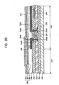
- FIG. 2A shows an embodiment of the planar structure of an organic light emitting display device without a pixel definition layer
- FIG. 2B is a cross-sectional view taken along the line II-II of FIG. 2A .
- a thin film transistor and a capacitor are formed on a non emission region 220 in the same manner and structure as illustrated in FIGS. 1A and 1B .
- a lower electrode 261 is formed by depositing a transparent conductive layer in the emission region on the entire surface of a substrate so as to contact a source/drain electrode formed in the non-emission region through a contact hole 258 for pixel electrode and H patterning the same.
- FIG. 2C is a perspective view showing the steps for forming the lower electrode 261
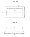
- FIG. 2D is a plan view of the lower electrode 261
- FIG. 2E is a cross-sectional view taken along the line III-III of FIG. 2D .
- corners of upper and lower portions of the lower electrode 261 are formed in an angle shape. As shown in FIG. 2E , a length L2 of the lower portion of the lower electrode 261 is formed longer than a length L1 of the upper portion of the lower electrode 261. That is, the lower electrode 261 has a side slanted at a tapered angle.
- An organic emission layer 262 is formed on the lower electrode 261. Then an upper electrode 263 made of a metallic material is formed on the organic emission layer.
- the organic emission layer 262 Upon the formation of the organic emission layer 262 on the lower electrode 261, a step is formed. However, in use, a short-induced defect may be generated due to an open edge phenomenon. Thus, in the case where the upper and lower portions of the transparent conductive layer are angled, the organic emission layer 262 often deteriorates at its corner portion to expose the lower electrode 261.
- embodiments of the invention provide a lower pixel electrode having rounded corners.
- FIG. 2F shows an enlarged view of an emission region upon the generation of a short-induced defect.
- EP1333497 (A2 ) teaches an organic electroluminescent display device, comprising a thin film transistor formed in a non-emission region on an insulating substrate and having source and drain electrodes; a lower electrode formed in an emission region on the insulating substrate and connected to one electrode of the source and drain electrodes through a contact hole; an organic emission layer formed in the emission region on the lower electrode; and an upper electrode formed on the organic emission layer
- JP3105893 (A ) discloses a thin film electroluminescent device having etched sharp parts of the surface of a transparent electrode and rounded the corner parts.
- US2003203527 (A1 ) discloses an active matrix OLED device, having an anode connected to the drain electrode of the TFT through a contact hole, an organic electroluminescent layer covering the anode electrode, and a cathode on the organic electroluminiscent layer.
- JP 2001 110575 A discloses an organic electroluminescent display device, comprising a lower electrode connected to the source of the TFT, whereby the side faces of the anode have a tapered incline that becomes broader to a lower layer.
- the present invention is directed to an improved organic electroluminescent display device that has no pixel definition layer.
- Embodiments of the present invention also provide a method for fabricating the same, which prevents outgassing and short-induced defects by forming a lower (e.g. pixel) electrode having corners that are rounded off.
- an organic electroluminescent display device in one embodiment, includes a thin film transistor formed in a non-emission region on an insulating substrate, which includes source/drain electrodes.
- the organic electroluminescent display device further includes a lower electrode formed in an emission region on the insulating substrate and connected to one electrode of the source/drain electrodes through a contact hole. It also includes an organic emission layer formed in the emission region on the lower electrode, and an upper electrode formed on the organic emission layer, wherein the lower electrode has a surface with its corners rounded off.
- the lower electrode has an upper surface in which a center of radius of curvature is at its corners so that the radius of curvature is zero, and a lower surface whose corners have curvature in which a center of radius of each curvature is at a point on the same axis as an axis on which a center of radius of curvature of the upper surface is positioned, wherein the axis is perpendicular to a plane on which the center of radius of each curvature of the upper surface is positioned so that the radius of each curvature of the lower surface is larger than zero.
- the lower electrode has an upper surface whose corners have curvature whose center is positioned on the upper surface, and a lower surface whose corners have curvature in which a center of radius of each curvature is at a point on the same axis as an axis on which a center of radius of curvature of the upper surface is positioned, wherein the axis is perpendicular to a plane including the center of the radius of each curvature of the upper surface, wherein the radius of each curvature of the lower surface is larger than that of the upper surface.
- the upper and the lower surface of the lower electrode has four corners and wherein in the first alternative curvature is formed at all four corners of the lower surface, respectively, and wherein in the second alternative curvature is formed at all four corners of the upper and lower surfaces, respectively.
- the upper electrode is a cathode electrode and the lower electrode is an
- a thin film transistor having source/drain electrodes is formed in a non-emission region on an insulating substrate.
- a lower electrode is formed in an emission region on the insulating substrate and connected to one electrode of the source/drain electrodes through a contact hole.
- the lower electrode has rounded corners.
- An organic emission layer is formed in the emission region on the lower electrode.
- An upper electrode is formed on the organic emission layer.
- the lower electrode has an upper surface in which a center of radius of curvature is at its corners so that the radius of curvature is zero, and a lower surface whose corners have curvature in which a center of radius of each curvature is at a point on the same axis as an axis on which a center of radius of curvature of the upper surface is positioned, wherein the axis is perpendicular to a plane on which the center of radius of each curvature of the upper surface is positioned so that the radius of each curvature of the lower surface is larger than zero.
- the lower electrode has an upper surface whose corners have curvature whose center is positioned on the upper surface, and a lower surface whose corners have curvature in which a center of radius of each curvature is at a point on the same axis as an axis on which a center of radius of curvature of the upper surface is positioned, wherein the axis is perpendicular to a plane including the center of the radius of each curvature of the upper surface, wherein the radius of each curvature of the lower surface is larger than that of the upper surface.
- the upper and the lower surface of the lower electrode has four corners, wherein in the first alternative curvature is formed at all four corners of the lower surface, respectively, and in the second alternative curvature is formed at all four corners of the upper and lower surfaces, respectively.
- FIG. 1A shows a planar structure of a conventional AMOLED
- FIG. 1B is a cross-sectional view taken along the line I-I of FIG. 1A ;
- FIG. 2A shows a planar structure of another conventional organic electroluminescent display device
- FIG. 2B is a cross-sectional view taken along the line II-II of FIG. 2A ;
- FIG. 2C is a perspective view showing steps for forming the lower electrode of FIG. 2A ;
- FIG. 2D is a plan view of the lower electrode of FIG. 2C ;
- FIG. 2E is a cross-sectional view taken along the line III-III of FIG. 2D ;
- FIG. 2F is an enlarged photograph of the emission region upon generation of the short-induced defect
- FIG. 3A shows a planar structure of an organic electroluminescent display device according to a first embodiment of the present invention
- FIG. 3B is a cross-sectional view taken along the line IV-IV of FIG. 3A ;
- FIG. 3C is a perspective view showing steps for forming the lower electrode of FIG. 3A ;
- FIG. 3D is a plan view of the lower electrode of FIG. 3C ;
- FIG. 3E is a cross-sectional view taken along the line V-V of FIG. 3D ;
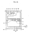
- FIG. 4A shows a planar structure of an organic electroluminescent display device according to a second embodiment of the present invention
- FIG. 4B is a perspective view showing steps for forming the lower electrode of FIG. 4A ;
- FIG. 4C is a plan view of the lower electrode of FIG. 4A ;
- FIG. 4D is a cross-sectional view taken along the line VII-VII of FIG. 4C .
- FIG. 3A shows a planar structure of an active matrix organic electroluminescent display device (AMOLED) according to a first embodiment of the present invention.
- the AMOLED of FIG. 3A illustrates a device consisting of two transistors and a capacitor.
- FIG. 3B shows a cross-sectional view taken along the line IV-IV of FIG. 3A .
- a buffer layer 340 is formed on a transparent insulating substrate 300, such as a glass substrate.
- the substrate includes a non-emission region 310 and an emission region 330.
- an amorphous silicon layer is deposited on the buffer layer 340 to form a semiconductor layer 311.
- the semiconductor layer 311 is formed by performing a crystallization process after patterning the amorphous silicon layer.
- a gate insulating layer 350 is formed on the entire surface of the substrate, and a metallic material for a gate electrode is deposited and patterned on the gate insulating layer 350 to form a gate 312 over the semiconductor layer 311.
- a capacitor lower electrode 322 is simultaneously formed at this time. Now, upon the formation of the gate 312 and the capacitor lower electrode 322, a gate line 302 of FIG. 3A is also formed.
- source/drain regions 313 and 314 are formed by ion implantation of, for example, P or N type impurities, into the semiconductor layer 311.
- an interlayer insulating layer 360 is formed on the entire surface of the substrate, and the interlayer insulating layer 360 and the gate insulating layer 350 are etched to expose a portion of the source/drain regions 313 and 314. Thereby, contact holes 361 and 362 for source/drain electrodes are formed.
- a metallic material for the source/drain electrodes is deposited on the interlayer insulating layer 360, the source/drain electrodes 315 and 316 are formed to contact with the source/drain regions 313 and 314 through the contact holes 361 and 362.
- a capacitor upper electrode 326 is formed which extends from any one electrode, for example, the source electrode 315, of the source/drain electrodes 315 and 316.
- a data line 304 and a power line 306 of FIG. 3A are also formed.
- a passivation layer 370 is formed on the interlayer insulating layer 360.
- the passivation layer 370 is etched to expose a portion of the other electrode, for example, the drain electrode 316, of the source/drain electrodes 315 and 316, thus forming a contact hole 371 for a pixel electrode.
- a transparent conductive layer is deposited on the passivation layer 370 in an emission region 330, and is patterned to form a lower electrode 331 contacting with the drain electrode 316 through the contact hole 371 for the pixel electrode.
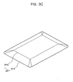
- FIGS. 3C to 3E steps for forming the lower electrode 331 of FIG. 3A are illustrated through FIGS. 3C to 3E .
- FIG. 3C is a perspective view showing a whole shape of the lower electrode 331
- FIG. 3D is a plan view of the lower electrode 331
- FIG. 3E is a cross-sectional view taken along the line V-V of FIG. 3D .
- the upper surface 331 a of the lower electrode 331 has a rectangular shape, and a lower surface 331b of the lower electrode 331 has rounded corners, so that the lower electrode 331 is tapered.
- 31 is the radius of curvature of the upper surface 331 a
- 32 is the radius of curvature of the lower surface 331b.
- the lower electrode 331 has the upper surface 331 a in which the center of the radius of curvature 31 is at its corners so that the radius of curvature is zero.
- the center of the radius of each curvature 32 of the lower surface 331b is located at a point on the same axis as an axis on which a center of radius of curvature of the upper surface is positioned, wherein the axis is perpendicular to a plane on which the center of the radius of each curvature of the upper surface 331 a is positioned so that the radius of each curvature 32 is larger than zero.
- upper surface 331 a has four angled corners and the lower surface 331b has four rounded corners. Accordingly, since the four corners of the lower surface of the lower electrode 331 are not angled, an open edge defect due to cut-off of the organic emission layer 332 can be prevented even after the organic emission layer 332 is deposited.
- an organic emission layer 332 is formed on the passivation layer 370 including the lower electrode 331.
- an upper electrode 333 made of a metallic material is formed thereon, thereby creating the active matrix organic electroluminescent display device.
- the lower electrode acts as an anode electrode and the upper electrode acts as a cathode electrode.
- FIG. 4A shows a planar structure of an active matrix organic electroluminescent display device (AMOLED) according to a second embodiment of the present invention.
- the AMOLED of FIG. 4A illustrates a device having two transistors and a capacitor.
- FIG. 4B A cross-sectional view taken along the line VI-VI of FIG. 4B illustrates structure similar to that shown in FIG. 3B . Additionally, a method of manufacturing the second embodiment of the present invention will be easily understood by a person skilled in the art with reference to the above description given with regard to the first embodiment. Thus, FIG. 4A need not be described in detail.
- FIG. 4B is a perspective view showing a whole shape of the lower electrode 431
- FIG. 4C is a plan view of the lower electrode 431
- FIG. 4D is a cross-sectional view taken along the line VII-VII of FIG. 4C .
- the lower electrode 431 Upon the formation of the lower electrode 431, shown in FIG. 4C , four corners of an inner portion of an upper surface 431a are rounded on a plane, four corners of an outer portion of a lower surface 431b are rounded. As shown in FIG. 4D , the lower electrode is formed to be tapered so that the lower surface 431 b is formed wider than upper surface 431 a.
- 41 is the radius of curvature of the upper surface 431 a of the lower electrode 431
- 42 is the radius of curvature of the lower surface 431b of the lower electrode 431.
- the lower electrode 431 has the upper surface 431a whose four corners each have curvature and the center of the curvature is positioned on the upper surface 431a.
- the center of the radius of curvature 42 of the lower surface 431b is at a point on the same axis as an axis on which a center of radius of curvature of the upper surface is positioned, wherein the axis is perpendicular to a plane including the center of the radius f each curvature 41 of the upper surface 431a, wherein the radius of each curvature 42 of the lower surface 431 b is larger than that of the upper surface 431a, and the four corners of the lower surface 431b are also rounded.
- the upper electrode (see 333 of FIG. 3B ) is formed on the organic emission layer (332 of FIG. 3B ) to supply a common power source.
- the lower electrode 431 is an anode electrode and the upper electrode formed on the organic emission layer is a cathode electrode.
- curvature of the lower electrode may also be provided at a side portion so that a shape of the surface of the lower electrode forms an oval or circular shape.
- the lower electrode in manufacturing an AMOLED having no pixel definition layer, is formed of a transparent metallic material and has the corners of its upper and lower surfaces rounded off, to prevent outgassing and short-induced defects.
- Such a configuration improves luminosity and increases the life of the organic electroluminescent display device.
Landscapes
- Physics & Mathematics (AREA)
- Optics & Photonics (AREA)
- Electroluminescent Light Sources (AREA)
- Devices For Indicating Variable Information By Combining Individual Elements (AREA)
Claims (5)
- Organische elektrolumineszente Anzeigevorrichtung, aufweisend:einen Dünnfilmtransistor, der in einer Nicht-Emissionsregion (310) auf einem Isoliersubstrat (300) ausgebildet ist und eine Source-Elektrode und eine Drain-Elektrode (315, 316) aufweist;eine untere Elektrode (331), die in einer Emissionsregion (330) auf dem Isoliersubstrat (300) ausgebildet ist und über ein Kontaktloch (317) mit einer Elektrode der Source-Elektrode und der Drain-Elektrode (315, 316) verbunden ist;eine organische Emissionsschicht (332), die in der Emissionsregion (330) auf der unteren Elektrode (331) ausgebildet ist; undeine obere Elektrode (333), die auf der organischen Emissionsschicht (332) ausgebildet ist,wobei die untere Elektrode (331) eine Oberfläche aufweist, deren Ecken abgerundet sind,dadurch gekennzeichnet, dass(i) die untere Elektrode (331) eine Oberseite (331a), bei der ein Mittelpunkt des Radius der Krümmung (p31) an ihren Ecken ist, sodass der Radius der Krümmung (p31) Null beträgt, und eine Unterseite (331b) aufweist, deren Ecken eine Krümmung aufweisen und bei der ein Mittelpunkt des Radius jeder Krümmung (p32) auf einem Punkt auf der selben Achse liegt wie eine Achse, auf der ein Mittelpunkt des Radius der Krümmung (p31) der Oberseite positioniert ist, wobei die Achse perpendikulär zu einer Ebene ist, auf der der Mittelpunkt des Radius jeder Krümmung (p31) der Oberseite derart positioniert ist, dass der Radius jeder Krümmung (p32) der Unterseite (331b) größer als Null ist, oder(ii) die untere Elektrode (431) eine Oberseite (431a), deren Ecken eine Krümmung aufweisen, deren Mittelpunkt auf der Oberseite (431a) positioniert ist, und eine Unterseite (431b) aufweist, deren Ecken eine Krümmung aufweisen und bei der ein Mittelpunkt des Radius jeder Krümmung (p42) auf einem Punkt auf der selben Achse liegt wie eine Achse, auf der ein Mittelpunkt des Radius der Krümmung (p41) der Oberseite (431a) positioniert ist, wobei die Achse perpendikulär zu einer Ebene ist, die der Mittelpunkt des Radius jeder Krümmung (p41) der Oberseite (431a) aufweist, wobei der Radius jeder Krümmung (p42) der Unterseite (431 b) größer als derjenige der Oberseite (431 a) ist.
- Organische elektrolumineszente Anzeigevorrichtung nach Anspruch 1, wobei die Ober- und die Unterseite (331 a; 331 b; 431 a; 431 b) der unteren Elektrode (331, 431) vier Ecken aufweist und wobei gemäß Alternative (i) die Krümmung jeweils an allen vier Ecken der Unterseite (331b) ausgebildet ist, und wobei gemäß Alternative (ii) die Krümmung jeweils an allen vier Ecken der Ober- und Unterseite (431 a; 431 b) ausgebildet ist.
- Organische elektrolumineszente Anzeigevorrichtung nach Alternative (i) von Anspruch 1, wobei die obere Elektrode (333) als Kathodenelektrode fungiert und die untere Elektrode (331; 431) als Anodenelektrode fungiert.
- Verfahren zur Herstellung einer organischen elektrolumineszenten Anzeigevorrichtung, wobei das Verfahren die folgenden Schritte aufweist:Ausbildung eines Dünnfilmtransistors, der eine Source-/Drain-Elektrode (315, 316) aufweist, in einer Nichtemissionsregion (310) auf einem Isoliersubstrat (300);Ausbildung einer unteren Elektrode (331) in einer Emissionsregion (330) auf dem Isoliersubstrat (300) derart, dass sie über ein Kontaktloch (317) mit einer Elektrode der Source-/Drain-Elekrode (315, 316) verbunden ist, wobei die untere Elektrode abgerundete Ecken aufweist,Ausbildung einer organischen Emissionsschicht (332) in der Emissionsregion (330) auf der unteren Elektrode (331); undAusbildung einer oberen Elektrode auf der organischen Emissionsschicht (332),dadurch gekennzeichnet, dass(i) die untere Elektrode (331) eine Oberseite (331 a) aufweist, bei der ein Mittelpunkt des Radius der Krümmung (p31) an ihren Ecken ist, sodass der Radius der Krümmung (p31) Null beträgt, und eine Unterseite (331b) aufweist, deren Ecken eine Krümmung aufweisen und bei der ein Mittelpunkt des Radius jeder Krümmung (p32) auf einem Punkt auf der selben Achse liegt wie eine Achse, auf der ein Mittelpunkt des Radius der Krümmung (p31) der Oberseite positioniert ist, wobei die Achse perpendikulär zu einer Ebene ist, auf der der Mittelpunkt des Radius jeder Krümmung (p31) der Oberseite positioniert ist, sodass der Radius jeder Krümmung (p32) der Unterseite (331 b) größer als Null ist, oder(ii) die untere Elektrode (431) eine Oberseite (431a), deren Ecken eine Krümmung aufweisen, deren Mittelpunkt auf der Oberseite (431a) positioniert ist, und eine Unterseite (431 b) aufweist, deren Ecken eine Krümmung aufweisen und bei der ein Mittelpunkt des Radius jeder Krümmung (p42) auf einem Punkt auf der selben Achse liegt wie eine Achse, auf der ein Mittelpunkt des Radius der Krümmung (p41) der Oberseite (431a) positioniert ist, wobei die Achse perpendikulär zu einer Ebene ist, die der Mittelpunkt des Radius jeder Krümmung (p41) der Oberseite (431a) aufweist, wobei der Radius jeder Krümmung (p42) der Unterseite (431b) größer als derjenige der Oberseite (431 a) ist.
- Verfahren nach Anspruch 4, wobei die Ober- und die Unterseite (331a; 331b; 431a; 431 b) der unteren Elektrode (331, 431) vier Ecken aufweist und wobei gemäß Alternative (i) die Krümmung jeweils an allen vier Ecken der Unterseite (331 b) ausgebildet ist, und wobei gemäß Alternative (ii) die Krümmung jeweils an allen vier Ecken der Ober- und Unterseite (431 a; 431 b) ausgebildet ist.
Applications Claiming Priority (2)
| Application Number | Priority Date | Filing Date | Title |
|---|---|---|---|
| KR1020030086154A KR100686341B1 (ko) | 2003-11-29 | 2003-11-29 | 유기전계발광 표시장치 및 그의 제조방법 |
| KR2003086154 | 2003-11-29 |
Publications (2)
| Publication Number | Publication Date |
|---|---|
| EP1536473A1 EP1536473A1 (de) | 2005-06-01 |
| EP1536473B1 true EP1536473B1 (de) | 2012-06-06 |
Family
ID=34464782
Family Applications (1)
| Application Number | Title | Priority Date | Filing Date |
|---|---|---|---|
| EP04090474A Expired - Lifetime EP1536473B1 (de) | 2003-11-29 | 2004-11-29 | Organische elektrolumineszente Anzeigevorrichtung und Herstellungsverfahren |
Country Status (5)
| Country | Link |
|---|---|
| US (1) | US7294962B2 (de) |
| EP (1) | EP1536473B1 (de) |
| JP (1) | JP2005327694A (de) |
| KR (1) | KR100686341B1 (de) |
| CN (1) | CN100440574C (de) |
Families Citing this family (16)
| Publication number | Priority date | Publication date | Assignee | Title |
|---|---|---|---|---|
| JP2006120622A (ja) * | 2004-09-21 | 2006-05-11 | Canon Inc | 発光スクリーン構造及び画像形成装置 |
| WO2007058183A1 (en) * | 2005-11-18 | 2007-05-24 | Semiconductor Energy Laboratory Co., Ltd. | Photoelectric conversion device |
| EP2629590A1 (de) * | 2008-06-17 | 2013-08-21 | Hitachi Ltd. | Organische lichtemittierende Vorrichtung |
| KR101108164B1 (ko) * | 2010-02-03 | 2012-02-06 | 삼성모바일디스플레이주식회사 | 유기 발광 표시 장치 |
| KR101084198B1 (ko) * | 2010-02-24 | 2011-11-17 | 삼성모바일디스플레이주식회사 | 유기 발광 표시 장치 |
| US9012927B2 (en) | 2011-11-30 | 2015-04-21 | Canon Kabushiki Kaisha | Display device |
| KR20140128080A (ko) | 2013-04-26 | 2014-11-05 | 삼성디스플레이 주식회사 | 유기 발광 표시 장치 및 그 제조 방법 |
| GB201500748D0 (en) | 2015-01-16 | 2015-03-04 | Cambridge Display Tech Ltd | Method of forming a light-emitting device |
| KR102368849B1 (ko) * | 2015-07-30 | 2022-02-28 | 엘지디스플레이 주식회사 | 유기전계발광표시장치 |
| US10593657B2 (en) * | 2016-11-01 | 2020-03-17 | Innolux Corporation | Display devices and methods for forming the same |
| CN108054184B (zh) * | 2017-12-11 | 2020-12-25 | 京东方科技集团股份有限公司 | 一种阵列基板及制备方法、显示装置 |
| CN109243305B (zh) * | 2018-09-17 | 2021-10-12 | 京东方科技集团股份有限公司 | 显示面板、显示装置和显示面板的制造方法 |
| KR102184724B1 (ko) * | 2019-12-31 | 2020-12-01 | 엘지디스플레이 주식회사 | 표시 장치 및 그의 제조 방법 |
| JP7477067B2 (ja) * | 2020-05-09 | 2024-05-01 | 京東方科技集團股▲ふん▼有限公司 | 表示パネル及びその製作方法、表示装置及びその製作方法 |
| JPWO2023042027A1 (de) * | 2021-09-16 | 2023-03-23 | ||
| US20240407211A1 (en) * | 2021-09-30 | 2024-12-05 | Semiconductor Energy Laboratory Co., Ltd. | Display device |
Citations (1)
| Publication number | Priority date | Publication date | Assignee | Title |
|---|---|---|---|---|
| JP2001110575A (ja) * | 1999-10-04 | 2001-04-20 | Sanyo Electric Co Ltd | エレクトロルミネッセンス表示装置 |
Family Cites Families (9)
| Publication number | Priority date | Publication date | Assignee | Title |
|---|---|---|---|---|
| JPH03105893A (ja) | 1989-09-19 | 1991-05-02 | Fuji Electric Co Ltd | 薄膜エレクトロルミネッセンス素子の製造方法 |
| EP0907304B1 (de) | 1996-05-29 | 2002-11-06 | Idemitsu Kosan Company Limited | Organische elektrolumineszente vorrichtung |
| JP3711682B2 (ja) * | 1997-03-07 | 2005-11-02 | セイコーエプソン株式会社 | 有機elディスプレイ |
| KR100316271B1 (ko) * | 1999-05-27 | 2001-12-12 | 구본준, 론 위라하디락사 | 전계발광소자 및 그의 제조방법 |
| JP2003022035A (ja) | 2001-07-10 | 2003-01-24 | Sharp Corp | 有機elパネルおよびその製造方法 |
| JP2003076332A (ja) * | 2001-08-31 | 2003-03-14 | Sanyo Electric Co Ltd | 表示パネルの駆動回路 |
| US20030214042A1 (en) * | 2002-02-01 | 2003-11-20 | Seiko Epson Corporation | Circuit substrate, electro-optical device and electronic appliances |
| JP2003332082A (ja) * | 2002-05-15 | 2003-11-21 | Victor Co Of Japan Ltd | 有機エレクトロルミネセンス素子 |
| JP4062171B2 (ja) * | 2003-05-28 | 2008-03-19 | ソニー株式会社 | 積層構造の製造方法 |
-
2003
- 2003-11-29 KR KR1020030086154A patent/KR100686341B1/ko not_active Expired - Fee Related
-
2004
- 2004-06-23 JP JP2004185199A patent/JP2005327694A/ja active Pending
- 2004-09-10 US US10/937,294 patent/US7294962B2/en not_active Expired - Lifetime
- 2004-09-29 CN CNB2004100117914A patent/CN100440574C/zh not_active Expired - Lifetime
- 2004-11-29 EP EP04090474A patent/EP1536473B1/de not_active Expired - Lifetime
Patent Citations (2)
| Publication number | Priority date | Publication date | Assignee | Title |
|---|---|---|---|---|
| JP2001110575A (ja) * | 1999-10-04 | 2001-04-20 | Sanyo Electric Co Ltd | エレクトロルミネッセンス表示装置 |
| US6727871B1 (en) * | 1999-10-04 | 2004-04-27 | Sanyo Electric Co., Ltd. | Electroluminescence display apparatus |
Also Published As
| Publication number | Publication date |
|---|---|
| CN1622728A (zh) | 2005-06-01 |
| KR100686341B1 (ko) | 2007-02-22 |
| KR20050052290A (ko) | 2005-06-02 |
| US20050116623A1 (en) | 2005-06-02 |
| US7294962B2 (en) | 2007-11-13 |
| EP1536473A1 (de) | 2005-06-01 |
| CN100440574C (zh) | 2008-12-03 |
| JP2005327694A (ja) | 2005-11-24 |
Similar Documents
| Publication | Publication Date | Title |
|---|---|---|
| EP1536473B1 (de) | Organische elektrolumineszente Anzeigevorrichtung und Herstellungsverfahren | |
| US7492096B2 (en) | Flat panel display device capable of reducing or preventing a voltage drop and method of fabricating the same | |
| US20060097263A1 (en) | Organic electroluminescent display device | |
| CN106992185B (zh) | 薄膜晶体管基板、包括其的显示器及其制造方法 | |
| JP2006286600A (ja) | 発光表示装置及び発光表示装置の製造方法 | |
| EP1599073B1 (de) | Organische EL Anzeigevorrichtung und ihr Herstellungsverfahren | |
| US7420324B2 (en) | Organic EL display and fabricating method thereof | |
| JP2005107492A (ja) | エレクトロルミネセンスディスプレイ装置 | |
| JP2003257645A (ja) | 発光装置およびその製造方法 | |
| JP4103373B2 (ja) | エレクトロルミネッセンス表示装置およびエレクトロルミネッセンス表示装置の製造方法 | |
| CN100372145C (zh) | 有机发光元件的制造方法及其结构 | |
| KR100617193B1 (ko) | 양방향 유기 el 디스플레이 소자 및 그 제조 방법 | |
| KR100741966B1 (ko) | 유기전계발광 표시장치 및 그의 제조방법 | |
| CN106953025B (zh) | 有机发光显示装置的制造方法 | |
| KR100638085B1 (ko) | 유기 전계 발광 표시장치 | |
| CN117479672A (zh) | 显示面板及显示面板的制造方法 | |
| KR20050115494A (ko) | 듀얼형 유기 el 디스플레이 패널 및 그 제조 방법 |
Legal Events
| Date | Code | Title | Description |
|---|---|---|---|
| PUAI | Public reference made under article 153(3) epc to a published international application that has entered the european phase |
Free format text: ORIGINAL CODE: 0009012 |
|
| 17P | Request for examination filed |
Effective date: 20041129 |
|
| AK | Designated contracting states |
Kind code of ref document: A1 Designated state(s): AT BE BG CH CY CZ DE DK EE ES FI FR GB GR HU IE IS IT LI LU MC NL PL PT RO SE SI SK TR |
|
| AX | Request for extension of the european patent |
Extension state: AL HR LT LV MK YU |
|
| RIN1 | Information on inventor provided before grant (corrected) |
Inventor name: KIM, KYONG-DO,LEGAL & IP TEAM CORP.PLANNING ST Inventor name: KIM, MU-HYUN,LEGAL & IP TEAM CORP. PLANNING ST |
|
| AKX | Designation fees paid |
Designated state(s): AT BE BG CH CY CZ DE DK EE ES FI FR GB GR HU IE IS IT LI LU MC NL PL PT RO SE SI SK TR |
|
| RAP1 | Party data changed (applicant data changed or rights of an application transferred) |
Owner name: SAMSUNG MOBILE DISPLAY CO., LTD. |
|
| REG | Reference to a national code |
Ref country code: DE Ref legal event code: R079 Ref document number: 602004038037 Country of ref document: DE Free format text: PREVIOUS MAIN CLASS: H01L0027000000 Ipc: H01L0027320000 |
|
| GRAP | Despatch of communication of intention to grant a patent |
Free format text: ORIGINAL CODE: EPIDOSNIGR1 |
|
| RIC1 | Information provided on ipc code assigned before grant |
Ipc: H01L 51/52 20060101ALI20120111BHEP Ipc: H01L 27/32 20060101AFI20120111BHEP |
|
| GRAS | Grant fee paid |
Free format text: ORIGINAL CODE: EPIDOSNIGR3 |
|
| GRAA | (expected) grant |
Free format text: ORIGINAL CODE: 0009210 |
|
| AK | Designated contracting states |
Kind code of ref document: B1 Designated state(s): AT BE BG CH CY CZ DE DK EE ES FI FR GB GR HU IE IS IT LI LU MC NL PL PT RO SE SI SK TR |
|
| REG | Reference to a national code |
Ref country code: GB Ref legal event code: FG4D |
|
| REG | Reference to a national code |
Ref country code: AT Ref legal event code: REF Ref document number: 561393 Country of ref document: AT Kind code of ref document: T Effective date: 20120615 Ref country code: CH Ref legal event code: EP |
|
| REG | Reference to a national code |
Ref country code: IE Ref legal event code: FG4D |
|
| REG | Reference to a national code |
Ref country code: DE Ref legal event code: R096 Ref document number: 602004038037 Country of ref document: DE Effective date: 20120802 |
|
| REG | Reference to a national code |
Ref country code: NL Ref legal event code: VDEP Effective date: 20120606 |
|
| REG | Reference to a national code |
Ref country code: DE Ref legal event code: R082 Ref document number: 602004038037 Country of ref document: DE Representative=s name: GULDE HENGELHAUPT ZIEBIG & SCHNEIDER, DE |
|
| PG25 | Lapsed in a contracting state [announced via postgrant information from national office to epo] |
Ref country code: CY Free format text: LAPSE BECAUSE OF FAILURE TO SUBMIT A TRANSLATION OF THE DESCRIPTION OR TO PAY THE FEE WITHIN THE PRESCRIBED TIME-LIMIT Effective date: 20120606 Ref country code: SE Free format text: LAPSE BECAUSE OF FAILURE TO SUBMIT A TRANSLATION OF THE DESCRIPTION OR TO PAY THE FEE WITHIN THE PRESCRIBED TIME-LIMIT Effective date: 20120606 Ref country code: FI Free format text: LAPSE BECAUSE OF FAILURE TO SUBMIT A TRANSLATION OF THE DESCRIPTION OR TO PAY THE FEE WITHIN THE PRESCRIBED TIME-LIMIT Effective date: 20120606 |
|
| REG | Reference to a national code |
Ref country code: AT Ref legal event code: MK05 Ref document number: 561393 Country of ref document: AT Kind code of ref document: T Effective date: 20120606 |
|
| PG25 | Lapsed in a contracting state [announced via postgrant information from national office to epo] |
Ref country code: GR Free format text: LAPSE BECAUSE OF FAILURE TO SUBMIT A TRANSLATION OF THE DESCRIPTION OR TO PAY THE FEE WITHIN THE PRESCRIBED TIME-LIMIT Effective date: 20120907 Ref country code: SI Free format text: LAPSE BECAUSE OF FAILURE TO SUBMIT A TRANSLATION OF THE DESCRIPTION OR TO PAY THE FEE WITHIN THE PRESCRIBED TIME-LIMIT Effective date: 20120606 |
|
| REG | Reference to a national code |
Ref country code: DE Ref legal event code: R082 Ref document number: 602004038037 Country of ref document: DE Representative=s name: GULDE HENGELHAUPT ZIEBIG & SCHNEIDER, DE Effective date: 20121026 Ref country code: DE Ref legal event code: R081 Ref document number: 602004038037 Country of ref document: DE Owner name: SAMSUNG DISPLAY CO., LTD., KR Free format text: FORMER OWNER: SAMSUNG SDI CO., LTD., SUWON, KR Effective date: 20120608 Ref country code: DE Ref legal event code: R081 Ref document number: 602004038037 Country of ref document: DE Owner name: SAMSUNG DISPLAY CO., LTD., KR Free format text: FORMER OWNER: SAMSUNG MOBILE DISPLAY CO., LTD., SUWON-SI, KR Effective date: 20121026 Ref country code: DE Ref legal event code: R081 Ref document number: 602004038037 Country of ref document: DE Owner name: SAMSUNG DISPLAY CO., LTD., YONGIN-CITY, KR Free format text: FORMER OWNER: SAMSUNG MOBILE DISPLAY CO., LTD., SUWON-SI, KYONGGI-DO, KR Effective date: 20121026 Ref country code: DE Ref legal event code: R081 Ref document number: 602004038037 Country of ref document: DE Owner name: SAMSUNG DISPLAY CO., LTD., YONGIN-CITY, KR Free format text: FORMER OWNER: SAMSUNG SDI CO., LTD., SUWON, KYONGGI-DO, KR Effective date: 20120608 Ref country code: DE Ref legal event code: R082 Ref document number: 602004038037 Country of ref document: DE Representative=s name: GULDE & PARTNER PATENT- UND RECHTSANWALTSKANZL, DE Effective date: 20121026 |
|
| REG | Reference to a national code |
Ref country code: GB Ref legal event code: 732E Free format text: REGISTERED BETWEEN 20130103 AND 20130109 |
|
| PG25 | Lapsed in a contracting state [announced via postgrant information from national office to epo] |
Ref country code: NL Free format text: LAPSE BECAUSE OF FAILURE TO SUBMIT A TRANSLATION OF THE DESCRIPTION OR TO PAY THE FEE WITHIN THE PRESCRIBED TIME-LIMIT Effective date: 20120606 Ref country code: CZ Free format text: LAPSE BECAUSE OF FAILURE TO SUBMIT A TRANSLATION OF THE DESCRIPTION OR TO PAY THE FEE WITHIN THE PRESCRIBED TIME-LIMIT Effective date: 20120606 Ref country code: IS Free format text: LAPSE BECAUSE OF FAILURE TO SUBMIT A TRANSLATION OF THE DESCRIPTION OR TO PAY THE FEE WITHIN THE PRESCRIBED TIME-LIMIT Effective date: 20121006 Ref country code: BE Free format text: LAPSE BECAUSE OF FAILURE TO SUBMIT A TRANSLATION OF THE DESCRIPTION OR TO PAY THE FEE WITHIN THE PRESCRIBED TIME-LIMIT Effective date: 20120606 Ref country code: EE Free format text: LAPSE BECAUSE OF FAILURE TO SUBMIT A TRANSLATION OF THE DESCRIPTION OR TO PAY THE FEE WITHIN THE PRESCRIBED TIME-LIMIT Effective date: 20120606 Ref country code: SK Free format text: LAPSE BECAUSE OF FAILURE TO SUBMIT A TRANSLATION OF THE DESCRIPTION OR TO PAY THE FEE WITHIN THE PRESCRIBED TIME-LIMIT Effective date: 20120606 Ref country code: AT Free format text: LAPSE BECAUSE OF FAILURE TO SUBMIT A TRANSLATION OF THE DESCRIPTION OR TO PAY THE FEE WITHIN THE PRESCRIBED TIME-LIMIT Effective date: 20120606 Ref country code: RO Free format text: LAPSE BECAUSE OF FAILURE TO SUBMIT A TRANSLATION OF THE DESCRIPTION OR TO PAY THE FEE WITHIN THE PRESCRIBED TIME-LIMIT Effective date: 20120606 |
|
| PG25 | Lapsed in a contracting state [announced via postgrant information from national office to epo] |
Ref country code: PT Free format text: LAPSE BECAUSE OF FAILURE TO SUBMIT A TRANSLATION OF THE DESCRIPTION OR TO PAY THE FEE WITHIN THE PRESCRIBED TIME-LIMIT Effective date: 20121008 Ref country code: PL Free format text: LAPSE BECAUSE OF FAILURE TO SUBMIT A TRANSLATION OF THE DESCRIPTION OR TO PAY THE FEE WITHIN THE PRESCRIBED TIME-LIMIT Effective date: 20120606 Ref country code: IT Free format text: LAPSE BECAUSE OF FAILURE TO SUBMIT A TRANSLATION OF THE DESCRIPTION OR TO PAY THE FEE WITHIN THE PRESCRIBED TIME-LIMIT Effective date: 20120606 |
|
| REG | Reference to a national code |
Ref country code: FR Ref legal event code: TP Owner name: SAMSUNG DISPLAY CO., LTD., KR Effective date: 20130130 |
|
| PLBE | No opposition filed within time limit |
Free format text: ORIGINAL CODE: 0009261 |
|
| STAA | Information on the status of an ep patent application or granted ep patent |
Free format text: STATUS: NO OPPOSITION FILED WITHIN TIME LIMIT |
|
| PG25 | Lapsed in a contracting state [announced via postgrant information from national office to epo] |
Ref country code: DK Free format text: LAPSE BECAUSE OF FAILURE TO SUBMIT A TRANSLATION OF THE DESCRIPTION OR TO PAY THE FEE WITHIN THE PRESCRIBED TIME-LIMIT Effective date: 20120606 Ref country code: ES Free format text: LAPSE BECAUSE OF FAILURE TO SUBMIT A TRANSLATION OF THE DESCRIPTION OR TO PAY THE FEE WITHIN THE PRESCRIBED TIME-LIMIT Effective date: 20120917 |
|
| 26N | No opposition filed |
Effective date: 20130307 |
|
| REG | Reference to a national code |
Ref country code: CH Ref legal event code: PL |
|
| REG | Reference to a national code |
Ref country code: DE Ref legal event code: R097 Ref document number: 602004038037 Country of ref document: DE Effective date: 20130307 |
|
| PG25 | Lapsed in a contracting state [announced via postgrant information from national office to epo] |
Ref country code: BG Free format text: LAPSE BECAUSE OF FAILURE TO SUBMIT A TRANSLATION OF THE DESCRIPTION OR TO PAY THE FEE WITHIN THE PRESCRIBED TIME-LIMIT Effective date: 20120906 Ref country code: LI Free format text: LAPSE BECAUSE OF NON-PAYMENT OF DUE FEES Effective date: 20121130 Ref country code: CH Free format text: LAPSE BECAUSE OF NON-PAYMENT OF DUE FEES Effective date: 20121130 |
|
| REG | Reference to a national code |
Ref country code: IE Ref legal event code: MM4A |
|
| PG25 | Lapsed in a contracting state [announced via postgrant information from national office to epo] |
Ref country code: IE Free format text: LAPSE BECAUSE OF NON-PAYMENT OF DUE FEES Effective date: 20121129 |
|
| PG25 | Lapsed in a contracting state [announced via postgrant information from national office to epo] |
Ref country code: MC Free format text: LAPSE BECAUSE OF NON-PAYMENT OF DUE FEES Effective date: 20121130 Ref country code: TR Free format text: LAPSE BECAUSE OF FAILURE TO SUBMIT A TRANSLATION OF THE DESCRIPTION OR TO PAY THE FEE WITHIN THE PRESCRIBED TIME-LIMIT Effective date: 20120606 |
|
| PG25 | Lapsed in a contracting state [announced via postgrant information from national office to epo] |
Ref country code: LU Free format text: LAPSE BECAUSE OF NON-PAYMENT OF DUE FEES Effective date: 20121129 |
|
| PG25 | Lapsed in a contracting state [announced via postgrant information from national office to epo] |
Ref country code: HU Free format text: LAPSE BECAUSE OF FAILURE TO SUBMIT A TRANSLATION OF THE DESCRIPTION OR TO PAY THE FEE WITHIN THE PRESCRIBED TIME-LIMIT Effective date: 20041129 |
|
| REG | Reference to a national code |
Ref country code: FR Ref legal event code: PLFP Year of fee payment: 12 |
|
| REG | Reference to a national code |
Ref country code: FR Ref legal event code: PLFP Year of fee payment: 13 |
|
| REG | Reference to a national code |
Ref country code: FR Ref legal event code: PLFP Year of fee payment: 14 |
|
| REG | Reference to a national code |
Ref country code: FR Ref legal event code: PLFP Year of fee payment: 15 |
|
| REG | Reference to a national code |
Ref country code: DE Ref legal event code: R079 Ref document number: 602004038037 Country of ref document: DE Free format text: PREVIOUS MAIN CLASS: H01L0027320000 Ipc: H10K0059000000 |
|
| P01 | Opt-out of the competence of the unified patent court (upc) registered |
Effective date: 20230515 |
|
| PGFP | Annual fee paid to national office [announced via postgrant information from national office to epo] |
Ref country code: GB Payment date: 20231023 Year of fee payment: 20 |
|
| PGFP | Annual fee paid to national office [announced via postgrant information from national office to epo] |
Ref country code: FR Payment date: 20231024 Year of fee payment: 20 Ref country code: DE Payment date: 20231023 Year of fee payment: 20 |
|
| REG | Reference to a national code |
Ref country code: DE Ref legal event code: R071 Ref document number: 602004038037 Country of ref document: DE |
|
| REG | Reference to a national code |
Ref country code: GB Ref legal event code: PE20 Expiry date: 20241128 |
|
| PG25 | Lapsed in a contracting state [announced via postgrant information from national office to epo] |
Ref country code: GB Free format text: LAPSE BECAUSE OF EXPIRATION OF PROTECTION Effective date: 20241128 |
|
| PG25 | Lapsed in a contracting state [announced via postgrant information from national office to epo] |
Ref country code: GB Free format text: LAPSE BECAUSE OF EXPIRATION OF PROTECTION Effective date: 20241128 |