EP1533743B1 - Détecteur d'empreintes digitales et sa méthode de fabrication - Google Patents
Détecteur d'empreintes digitales et sa méthode de fabrication Download PDFInfo
- Publication number
- EP1533743B1 EP1533743B1 EP20040255047 EP04255047A EP1533743B1 EP 1533743 B1 EP1533743 B1 EP 1533743B1 EP 20040255047 EP20040255047 EP 20040255047 EP 04255047 A EP04255047 A EP 04255047A EP 1533743 B1 EP1533743 B1 EP 1533743B1
- Authority
- EP
- European Patent Office
- Prior art keywords
- fingerprint
- fingerprint sensor
- insulating layer
- type dopant
- lower electrode
- Prior art date
- Legal status (The legal status is an assumption and is not a legal conclusion. Google has not performed a legal analysis and makes no representation as to the accuracy of the status listed.)
- Expired - Lifetime
Links
Images


Classifications
-
- G—PHYSICS
- G06—COMPUTING OR CALCULATING; COUNTING
- G06V—IMAGE OR VIDEO RECOGNITION OR UNDERSTANDING
- G06V40/00—Recognition of biometric, human-related or animal-related patterns in image or video data
- G06V40/10—Human or animal bodies, e.g. vehicle occupants or pedestrians; Body parts, e.g. hands
- G06V40/12—Fingerprints or palmprints
- G06V40/13—Sensors therefor
- G06V40/1306—Sensors therefor non-optical, e.g. ultrasonic or capacitive sensing
Definitions
- the present invention relates to a fingerprint sensor and a fabrication method thereof, and more particularly, to a fingerprint sensor adopting a complementary metal-oxide semiconductor (CMOS) structure on which a piezoelectric region for generating ultrasonic waves is formed, so as to be fabricated using a simple process and to authenticate a fingerprint at a high speed.
- CMOS complementary metal-oxide semiconductor
- a security system generally adopts a personal authentication method using biometric technology, i.e., fingerprint sensing technology.
- a fingerprint sensing system includes a fingerprint scanner, i.e., a fingerprint sensor, and a signal processing algorithm. The fingerprint sensing system must have a high sensing rate and a low error rate to obtain a high-quality image of a fingerprint. A high-performance fingerprint sensor is necessary for this high-quality image of the fingerprint.
- a fingerprint sensor is generally classified as an optical type sensor, a capacitive type sensor, an ultrasonic type sensor, and the like.
- the optical type of fingerprint sensor is convenient to use but is relatively high-priced, sensitive to the dry or moist state of the fingerprint part of a finger to cause inexact fingerprint sensing, and may sense a false fingerprint as a true fingerprint.
- the capacitive type fingerprint sensor is lower priced than the optical type fingerprint sensor, compact, and highly stable but sensitive to the dry or moist state of the fingerprint part of the finger.
- the ultrasonic type fingerprint sensor can obtain reliable sensing results regardless of the state of the fingerprint part of the finger.
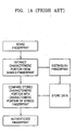
- An ultrasonic type fingerprint sensing system generally follows a fingerprint authentication process shown in FIG. 1A.
- the ultrasonic type fingerprint sensing system senses a fingerprint using a fingerprint sensor, extracts a characteristic portion from the sensed fingerprint, and stores the characteristic portion in a database (DB) to be used to distinguish the fingerprint from different types of fingerprints.
- the ultrasonic type fingerprint sensing system compares a characteristic portion of a fingerprint obtained during fingerprint authentication with the characteristic portion of the fingerprint stored in the DB to authenticate the obtained fingerprint.
- FIG. 1B is a cross-sectional view of an ultrasonic type fingerprint sensor disclosed in U.S. Pat. No. 5,587,533.
- an ultrasonic transducer 140, a mirror 156, a motor 160, an actuator 154, and a signal processor are separately fabricated and then put together.
- the ultrasonic type fingerprint sensor adopts a separately fabricated probe 102, which scans a fingerprint, and thus is costly and not easily applied to portable terminals.
- the ultrasonic type fingerprint sensor obtains an image of a fingerprint using a scan method, resulting in slow fingerprint authentication.
- a fingerprint sensor using ultrasonic waves includes: a complementary metal-oxide semiconductor structure which is formed on a substrate that is doped with a first type dopant; an insulating layer which is formed on the complementary metal-oxide semiconductor structure; a lower electrode which is formed in a central portion of the insulating layer; a piezoelectric region which is formed on the lower electrode; an upper electrode which is formed on the piezoelectric layer; and a fingerprint contact layer which is formed to cover a portion of an upper surface of the insulating layer on which the lower electrode has not been formed, the lower electrode, the piezoelectric region, and the upper electrode.
- the present invention provides a fingerprint sensor of an ultrasonic type in which components can be fabricated together using a micro-electric mechanical system (MEMS) process to have a thin film shape so as to increase a fingerprint authentication speed, and a fabrication method thereof.
- MEMS micro-electric mechanical system
- the complementary metal-oxide semiconductor structure may include: a region which is formed in a portion of the surface of the substrate by doping with a second type dopant; a source and a drain which are formed in the surface of the region doped with the second type dopant by doping with the first type dopant; and a source and a drain which are formed in a portion of the surface of the substrate by doping the portion the second type dopant so as to be opposite to the source and the drain doped with the first type dopant.
- the lower electrode may be electrically connected to the drain doped with the first type dopant and the source doped with the second type dopant.
- the lower electrode may be electrically connected to the drain doped with the first type dopant and the source doped with the second type dopant through via holes which penetrate through the insulating layer and are filled with a conductive material.
- the piezoelectric region may include at least one of PZT, PST, Quartz, (Pb, Sm)TiO 3 , PMN(Pb(MgNb)O 3 )-PT(PbTiO 3 ), PVDF, and PVDF-TrFe.
- the fingerprint contact layer may include a material having a similar acoustic impedance to that of the skin tissue of a person's finger.
- the fingerprint contact layer may include at least one of polymer materials comprising polyurethane, polystyrene, and rubber.
- the fingerprint sensor may have a matrix structure in which unit elements are arrayed.
- a method of fabricating a fingerprint sensor using ultrasonic waves including: forming a complementary metal-oxide semiconductor structure on a substrate that is doped with a first type dopant; forming an insulating layer on the complementary metal-oxide semiconductor structure and sequentially forming a lower electrode, a piezoelectric region, and an upper electrode on the insulating layer; removing side portions of the lower electrode, the piezoelectric region, and the upper electrode; and forming a fingerprint contact layer to cover a portion of an upper surface of the insulating layer, the lower electrode, the piezoelectric region, and the upper electrode.
- the formation of the insulating layer may include: forming the insulating layer on the complementary metal-oxide semiconductor structure; forming first and second via holes in the insulating layer to respectively face a drain of the complementary metal-oxide semiconductor structure having the first polarity and a source of the complementary metal-oxide semiconductor structure having a second polarity and then filling the first and second via holes with a conductive material; and sequentially forming the lower electrode, the piezoelectric region, and the upper electrode on the insulating layer and the first and second via holes.
- the piezoelectric region may include at least one of PZT, PST, Quartz, (Pb, Sm)TiO 3 , PMN(Pb(MgNb)O 3 )-PT(PbTiO 3 ), PVDF, and PVDF-TrFe.
- the fingerprint contact layer may include at least one of polymer materials including polyurethane, polystyrene, and rubber that have a similar acoustic impedance to that of the skin tissue of a person's finger.
- FIG. 2 is a cross-sectional view of a fingerprint sensor according to an embodiment of the present invention.
- a CMOS structure in which a negative-channel metal-oxide semiconductor (NMOS) structure and a positive-channel metal-oxide semiconductor (PMOS) structure are formed on an n-type or p-type substrate is formed as a lower structure of the fingerprint sensor according to the present invention.
- NMOS negative-channel metal-oxide semiconductor
- PMOS positive-channel metal-oxide semiconductor
- An n-type source 22a and an n-type drain 22b are formed in the portion of the surface of the n-type substrate 21 in which the p-type doped layer 23 has been formed.
- a p-type source 24a and a p-type drain 24b are formed in a portion of the surface of the n-type substrate 21 opposite to the n-type source 22a and the n-type drain 22b.
- a thin first insulating layer 25a is formed on the n-type substrate 21.
- a first gate 27a is formed on the first insulating layer 25a to face the n-type source 22a and the n-type drain 22b.
- a second gate 27b is formed on the first insulating layer 25a to face the p-type source 24a and the p-type drain 24b.
- a first electrode 26a is formed on the first insulating layer 25a to be electrically connected to the n-type source 22a. For the electrical connection of the first electrode 26a with the n-type source 22a, a portion of the first insulating layer 25a beneath which the n-type source 22a has been formed is removed.
- a second electrode 26b is formed on the first insulating layer 25a to be electrically connected to the p-type drain 24b. For the electrical connection of the second electrode 26b with the p-type drain 24b, a portion of the first insulating layer 25a beneath which the p-type drain 24b has been formed is removed.
- a second insulating layer 25b is formed on the above-described CMOS structure, i.e., on the first insulating layer 25a, the first and second gates 27a and 27b, and the first and second electrodes 26a and 26b.
- First and second via holes 28a and 28b are formed to penetrate through portions of the first and second insulating layers 25a and 25b, underneath which the n-type drain 22b and the p-type source 24a have been formed.
- the first and second via holes 28a and 28b are filled with a conductive material.
- the resultant structure refers to the lower structure of the fingerprint sensor according to the present invention.
- the lower structure of the fingerprint sensor according to the present invention has a structure in which the first and second via holes 28a and 28b are formed to penetrate through the portions of the first and second insulating layers 25a and 25b, underneath which the n-type drain 22b and the p-type source 24a of the CMOS structure are formed, and then filled with the conductive material.
- a lower electrode 31 is formed on the central portion of the second insulating layer 25b but not the side portions of the second insulating layer 25b and is electrically connected to the conductive material of the first via holes 28a and 28b.
- a piezoelectric region 32 is formed on the lower electrode 31, and then an upper electrode 33 is formed on the piezoelectric region 32.
- a fingerprint contact layer 34 is formed to cover a portion of the upper surface of the second insulating layer 25b, the lower electrode 31, the piezoelectric region 32, and the upper electrode 33.
- the piezoelectric region 32 is generally formed of a piezoelectric material such as PZT or the like.
- the fingerprint contact layer 34 is formed so as to include a material having a similar acoustic impedance to that of the skin tissue of a person' s finger.
- the fingerprint contact layer 34 may be formed of a polymer material such as polyurethane, polystyrene, rubber, or the like.
- the fingerprint sensor according to the present invention includes lower and upper structures as described above.
- the lower and upper structures are unit elements of the fingerprint sensor.
- the fingerprint sensor according to the present invention may have an M ⁇ N matrix structure in which such unit elements are arrayed.
- the fingerprint sensor according to the present invention has a structure in which unit elements each including the lower electrode 31, the piezoelectric region 32, and the upper electrode 33 are arrayed on the lower structure.
- the size of the unit elements of the fingerprint sensor according to the present invention i.e., the width of the unit elements of the fingerprint sensor, is about 50mm or less.
- the resonant frequency in the unit elements of the fingerprint sensor must be 30MHZ or more.
- the size of the unit elements must be 50mm or less.
- FIG. 3A is a cross-sectional view showing the fingerprint part of the end of a finger contacting the surface of the fingerprint sensor according to the present invention.
- the piezoelectric region 32 generates ultrasonic waves due to power applied by the lower and upper electrodes 31 and 33.
- reference character A denotes a portion of the fingerprint part of a person's finger which does not contact the surface of the fingerprint contact layer 34 that faces a unit element in the fingerprint sensor according to the present invention.
- reference character A denotes a valley between ridges of the fingerprint part of the person's finger.
- the ultrasonic waves generated by the piezoelectric region 32 are mostly reflected from the surface of the fingerprint contact layer 34 and then return to the inside of the fingerprint sensor according to the present invention.
- Reference character B denotes a portion of the fingerprint part of the person's finger contacting the surface of a unit element of the fingerprint sensor according to the present invention.
- ridges of the fingerprint part of the person's finger have a similar acoustic impedance to that of the fingerprint contact layer 34 and thus pass some of the ultrasonic waves therethrough.
- a portion of the finger contact layer 34 does not contact the ridges of the fingerprint part of the person's finger, some of the ultrasonic waves are reflected from the portion of the fingerprint contact layer 34. This is shown in FIG. 3C.
- Reference character C of FJG. 3A denotes a ridge of the fingerprint part of a person's finger where ultrasonic waves are absorbed.
- FIG. 3D shows ultrasonic waves that are not reflected from but pass through the surface of the fingerprint contact layer 34.
- FIG. 3E is a circuit diagram showing the operation of the fingerprint sensor according to the present invention.
- the fingerprint sensor which contacts the fingerprint part of a person' s finger, receives a signal generated from the reflected ultrasonic waves and transmits the signal to a controller (not shown).
- a signal generated from each unit element of the fingerprint sensor having the array structure is analyzed and location values of portions of the fingerprint sensor contacting the ridges of the fingerprint part of a person's finger are calculated to detect a fingerprint.
- the detected fingerprint undergoes the fingerprint authentication process of FIG. 1A.
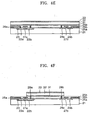
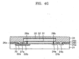
- FIGS. 4A through 4G An embodiment of a method of fabricating the fingerprint sensor according to the present invention will now be explained with reference to FIGS. 4A through 4G.
- FIGS. 4A through 4G are cross-sectional views explaining a method of fabricating a fingerprint sensor according to an embodiment of the present invention.
- FIG. 4A shows a general CMOS structure. Such a CMOS structure may be fabricated using a conventional method which will not be described here.
- a substrate 21 is doped with a dopant.
- an n-type or p-type substrate may be formed by doping it with an n-type or p-type dopant.
- the substrate 21 is n-type.
- a portion of the surface of the n-type substrate 21 is doped with a material having an opposite polarity to the n-type substrate 21, i.e., a second polarity.
- the portion of the surface of the n-type substrate 21 is doped with a p-type dopant to form a p-type doped layer 23.
- An n-type source 22a and an n-type drain 22b are formed in the surface of the n-type substrate 21 in which the p-type doped layer 23 has been formed.
- a p-type source 24a and a p-type drain 24b are formed in a portion of the surface of the n-type substrate 21 opposite to the n-type source 22a and the n-type drain 22b.
- a thin first insulating layer 25a is formed on the n-type substrate 21.
- a first gate 27a is formed on the first insulating layer 25a to face the n-type source 22a and the n-type drain 22b.
- a second gate 27b is formed on the first insulating layer 25a to face the p-type source 24a and the p-type drain 24b.
- a first electrode 26a is formed on the first insulating layer 25a to be electrically connected to the n-type source 22a. For the electrical connection of the first electrode 26a with the n-type source 22a, a portion of the first insulating layer 25a beneath which the n-type source 22a has been formed is removed.
- a second electrode 26b is formed on the first insulating layer 25a to be electrically connected to the p-type drain 24b. For the electrical connection of the second electrode 26b with the p-type drain 24b, a portion of the first insulating layer 25a beneath which the p-type drain 24b has been formed is removed.
- a second insulating layer 25b is formed on the first insulating layer 25a to a thickness of 0.01 - 1 ⁇ m and serves as a passivation layer.
- the second insulating layer 25b is formed of a silicon oxide film using plasma enhanced chemical vapor deposition (PECVD).
- PECVD plasma enhanced chemical vapor deposition
- portions of the second insulating layer 25b are removed up to the n-type drain 22b and the p-type source 24a using wet etching or reactive ion etching.
- the removal of the portions of the second insulating layer 25b results in forming first and second via holes 28a and 28b.
- the first and second via holes 28a and 28b are filled with a conductive material, for example, a metal such as tungsten or the like, using CVD or sputtering.
- a lower electrode 31 is formed of a metal such as Pt, Ti, Pd, Al, or Cu on the second insulating layer 25b, using sputtering or CVD, to a thickness of about 0.01 - 1 ⁇ m.
- the lower electrode 31 is covered with a piezoelectric material such as PZT, using a Sol-Gel process or sputtering, to form a piezoelectric region 32 having a thickness of about 0.5 - 20 ⁇ m.
- An upper electrode 33 is formed of a material such as Pt, Ti, Pd, Al, or Cu on the piezoelectric region 32, using sputtering or CVD, to have a thickness of about 0.01 - 1 ⁇ m.
- the piezoelectric region 32 is removed using lithography or etching, i.e., wet etching or reactive ion etching.
- the lower electrode 31 is connected to the conductive material which has filled the first and second via holes 28a and 28b.
- the piezoelectric region 32 is formed in a square shape to a width and length of about 50mm.
- lithography or etching makes the piezoelectric region 32 a predetermined size and the upper electrode 33 stripe-shaped so as to be connected to upper electrodes of other elements of the fingerprint sensor.
- the piezoelectric region 32 may be formed of a general piezoelectric material or an oxide-family or polymer-family piezoelectric material.
- a piezoelectric material may be PZT, PST, Quartz, (Pb, Sm)TiO 3 , PMN(Pb(MgNb)O 3 )-PT(PbTiO 3 ), PVDF, or PVDF-TrFe.
- a fingerprint contact layer 34 is formed to a thickness of about 10 ⁇ m or more using spin-coating or an e-beam to cover a portion of the upper surface of the second insulating layer 25b, the lower electrode 31, the piezoelectric region 32, and the upper electrode 33.
- the fingerprint contact layer 34 guides the path of ultrasonic waves generated by the piezoelectric region 32 and is formed of a material having a similar acoustic impedance to that of the skin tissue of a person's finger.
- the fingerprint contact layer 34 may be formed of a polymer material such as polyurethane, polystyrene, rubber, or the like. Accordingly, unit elements of the fingerprint sensor according to the present invention or an array type fingerprint sensor having an MxN matrix structure is completely fabricated.
- CMOS structure can be adopted to process a signal.
- piezoelectric region can be formed over the CMOS structure to generate ultrasonic waves.
- the fingerprint sensor can be simply fabricated.
- the fingerprint sensor can sense and authenticate a fingerprint at a high speed.
Landscapes
- Engineering & Computer Science (AREA)
- Human Computer Interaction (AREA)
- Physics & Mathematics (AREA)
- General Physics & Mathematics (AREA)
- Multimedia (AREA)
- Theoretical Computer Science (AREA)
- Image Input (AREA)
- Measurement Of The Respiration, Hearing Ability, Form, And Blood Characteristics Of Living Organisms (AREA)
- Metal-Oxide And Bipolar Metal-Oxide Semiconductor Integrated Circuits (AREA)
Claims (12)
- Un détecteur d'empreintes digitales utilisant des ondes ultrasons, comprenant :■ une structure à semi-conducteur à oxyde métallique complémentaire, formée sur un substrat ayant été dopé avec un premier type de dopant.■ Une couche isolante, formée sur la structure à semi-conducteur d'oxyde métallique complémentaire ;■ une électrode inférieure, formée dans une partie centrale de la couche isolante ;■ une région piézo-électrique, formée sur l'électrode inférieure ;■ une électrode supérieure, formée sur la couche piézo-électrique ; et■ une couche de contact d'empreinte digitale, formée pour couvrir une partie d'une surface supérieure de la couche isolante sur laquelle l'électrode inférieure n'a pas été formée, l'électrode inférieure, la région piézo-électrique, et l'électrode supérieure.
- Le détecteur d'empreintes digitales selon la revendication 1, dans lequel la structure à semi-conducteur à oxyde métallique complémentaire comprend :■ une région formée en une partie de la surface de substrat par dopage avec un deuxième type de dopant ;■ une source et un drain, formés dans la surface de la région ayant été dopée avec le deuxième type de dopant, en dopant avec le premier type de dopant, et■ une source et un drain, formés dans une partie de la surface du substrat par dopage de la portion avec le deuxième type de dopant, de manière à se trouver en regard de la source et du drain dopé avec le premier type de dopant.
- Le détecteur d'empreintes digitales selon la revendication 2, dans lequel l'électrode inférieure est connectée électriquement au drain, dopé avec le premier type de dopant, et à la source, dopée avec le deuxième type de dopant.
- Le détecteur d'empreintes digitales selon la revendication 3, dans lequel l'électrode inférieure est connectée électriquement au drain, dopé avec le premier type de dopant, et à la source dopée, avec le deuxième type de dopant, par des trous de traversée, pénétrant à travers la couche isolante et remplis d'un matériau conducteur.
- Le détecteur d'empreintes digitales selon l'une quelconque des revendications précédentes, dans lequel la région piézo-électrique comprend au moins l'un parmi PZT, PST, quartz, (Pb, Sm)-TiO3, PMN(Pb(MgNb)O3)-PT(PbTiO3), PVDF, et PVDF-TrFe.
- Le détecteur d'empreintes digitales selon l'une quelconque des revendications précédentes, dans lequel la couche de contact d'empreintes digitales comprend un matériau ayant une impédance acoustique similaire à celle du tissu de la peau du doigt d'une personne.
- Le détecteur d'empreintes digitales selon la revendication 6, dans lequel la couche de contact d'empreintes digitales comprend au moins l'un de matériaux polymères comprenant le polyuréthane, le polystyrène et le caoutchouc.
- Le détecteur d'empreintes digitales selon l'une quelconque des revendications précédentes, dans lequel le détecteur d'empreintes digitales comprend une structure matricielle, dans laquelle sont agencés en matrices des éléments unitaires.
- Un procédé de fabrication d'un détecteur d'empreintes digitales utilisant des ondes ultrasons, comprenant .■ la formation d'une structure à semi-conducteur de type oxyde métallique complémentaire sur un substrat dopé avec un premier type de dopant ;■ la formation d'une couche isolante sur la structure à semi-conducteur d'oxyde métallique complémentaire et, séquentiellement, la formation d'une électrode inférieure, d'une région piézo-électrique et d'une électrode supérieure sur la couche isolante ;■ l'élimination des parties latérales de l'électrode inférieure, de la région piézo-électrique, et de l'électrode supérieure ; et■ la formation d'une couche de contact d'empreintes digitales, pour couvrir une portion d'une surface supérieure de la couche isolante, de l'électrode inférieure, de la région piézo-électrique et de l'électrode supérieure.
- Le procédé selon la revendication 9 dans lequel la formation de la couche isolante comprend :■ la formation de la couche isolante sur la structure à semi-conducteur à oxyde métallique complémentaire ;■ la formation de premier et deuxième trous de traversée dans la couche isolante, pour être respectivement placés face à un drain de la structure à semi-conducteur à oxyde métallique complémentaire, ayant la première polarité, et une source de la structure à semi-conducteur à oxyde métallique complémentaire, ayant une deuxième polarité, et, ensuite, le remplissage des premier et deuxième trous de traversée par un matériau conducteur ; et■ séquentiellement, la formation de l'électrode inférieure de la région piézo-électrique et de l'électrode supérieure, sur la couche isolante, et les premier et deuxième trous de traversée.
- Le procédé selon la revendication 9 ou 10, dans lequel, la régio piézo-électrique comprend au moins l'un parmi PZT, PST, quartz, (Pb, Sm)TiO3, PMN(Pb(MgNb)O3-PT(PbTiO3), PVDF, et PVDF-TrFe.
- Le procédé selon la revendication 9, 10 ou 11 dans lequel la couche de contact d'empreinte digitale comprend au moins l'un des matériaux polymères comprenant le polyuréthane, le polystyrène et le caoutchouc, ayant une impédance acoustique similaire à celle du tissu de la peau du doigt d'une personne.
Applications Claiming Priority (2)
| Application Number | Priority Date | Filing Date | Title |
|---|---|---|---|
| KR2003081724 | 2003-11-18 | ||
| KR20030081724A KR100561851B1 (ko) | 2003-11-18 | 2003-11-18 | 지문 인식 센서 및 그 제조 방법 |
Publications (2)
| Publication Number | Publication Date |
|---|---|
| EP1533743A1 EP1533743A1 (fr) | 2005-05-25 |
| EP1533743B1 true EP1533743B1 (fr) | 2006-04-19 |
Family
ID=36314089
Family Applications (1)
| Application Number | Title | Priority Date | Filing Date |
|---|---|---|---|
| EP20040255047 Expired - Lifetime EP1533743B1 (fr) | 2003-11-18 | 2004-08-20 | Détecteur d'empreintes digitales et sa méthode de fabrication |
Country Status (6)
| Country | Link |
|---|---|
| US (1) | US7400750B2 (fr) |
| EP (1) | EP1533743B1 (fr) |
| JP (1) | JP4223465B2 (fr) |
| KR (1) | KR100561851B1 (fr) |
| CN (1) | CN100378997C (fr) |
| DE (1) | DE602004000683T2 (fr) |
Families Citing this family (140)
| Publication number | Priority date | Publication date | Assignee | Title |
|---|---|---|---|---|
| WO2006042144A2 (fr) * | 2004-10-07 | 2006-04-20 | Ultra-Scan Corporation | Balayage par ultrasons d'une empreinte digitale avec emploi d'une onde plane |
| US7558410B2 (en) * | 2004-12-01 | 2009-07-07 | Ultra-Scan Corporation | Fingerprint scanning station |
| US7738681B1 (en) * | 2005-11-01 | 2010-06-15 | Hewlett-Packard Development Company, L.P. | Fingerprint and physical attribute detection |
| KR100798481B1 (ko) * | 2006-11-15 | 2008-01-28 | 한국표준과학연구원 | 표면압력감지방식의 지문인식장치 |
| CN100514659C (zh) * | 2007-01-15 | 2009-07-15 | 南茂科技股份有限公司 | 指纹辨识器的薄膜封装构造 |
| CN100590643C (zh) * | 2007-01-17 | 2010-02-17 | 南茂科技股份有限公司 | 指纹辨识器的薄膜封装构造 |
| KR100867223B1 (ko) * | 2007-01-17 | 2008-11-06 | 경상대학교산학협력단 | 압전 센서를 이용한 개인인증 장치 및 방법 |
| CN101663558B (zh) * | 2007-04-05 | 2011-06-22 | 富士通半导体股份有限公司 | 表面形状传感器及其制造方法 |
| US20080258580A1 (en) * | 2007-04-20 | 2008-10-23 | Schneider John K | Reliability Improvement For Piezoelectric Imaging Array Device |
| US8805031B2 (en) * | 2008-05-08 | 2014-08-12 | Sonavation, Inc. | Method and system for acoustic impediography biometric sensing |
| US8331633B2 (en) * | 2008-05-08 | 2012-12-11 | Sonavation, Inc. | Method and system for multi-mode mechanical resonator |
| CN101875480B (zh) * | 2009-03-30 | 2014-09-17 | Nxp股份有限公司 | 前端微腔 |
| US8201739B2 (en) * | 2010-03-08 | 2012-06-19 | Ultra-Scan Corporation | Biometric sensor with delay layer |
| WO2011143279A1 (fr) | 2010-05-11 | 2011-11-17 | Ultra-Scan Corporation | Imagerie longitudinale réflexe à l'aide d'insonation ultrasonique par des capteurs |
| US9911911B2 (en) * | 2010-06-01 | 2018-03-06 | Qualcomm Incorporated | Multiple electrode plane wave generator |
| WO2011153188A1 (fr) * | 2010-06-01 | 2011-12-08 | Ultra-Scan Corporation | Générateur d'ondes planes à électrodes multiples |
| US9259961B2 (en) * | 2010-12-10 | 2016-02-16 | Palo Alto Research Center Incorporated | Large-area ultrasound contact imaging |
| CN102670241B (zh) * | 2011-03-17 | 2014-12-10 | 周正三 | 主动式生物特征感测器及使用其的电子装置 |
| KR101288178B1 (ko) * | 2011-11-30 | 2013-07-19 | 삼성전기주식회사 | 지문 인식 센서 및 지문 인식 방법 |
| US9633247B2 (en) | 2012-03-01 | 2017-04-25 | Apple Inc. | Electronic device with shared near field communications and sensor structures |
| KR101435450B1 (ko) * | 2012-11-26 | 2014-08-28 | (주)와이솔 | 지문 인식용 센서 패키지 및 그 제조 방법 |
| US10497747B2 (en) | 2012-11-28 | 2019-12-03 | Invensense, Inc. | Integrated piezoelectric microelectromechanical ultrasound transducer (PMUT) on integrated circuit (IC) for fingerprint sensing |
| US9618405B2 (en) | 2014-08-06 | 2017-04-11 | Invensense, Inc. | Piezoelectric acoustic resonator based sensor |
| US9511994B2 (en) | 2012-11-28 | 2016-12-06 | Invensense, Inc. | Aluminum nitride (AlN) devices with infrared absorption structural layer |
| US10726231B2 (en) | 2012-11-28 | 2020-07-28 | Invensense, Inc. | Integrated piezoelectric microelectromechanical ultrasound transducer (PMUT) on integrated circuit (IC) for fingerprint sensing |
| US9114977B2 (en) | 2012-11-28 | 2015-08-25 | Invensense, Inc. | MEMS device and process for RF and low resistance applications |
| US20140355387A1 (en) | 2013-06-03 | 2014-12-04 | Qualcomm Incorporated | Ultrasonic receiver with coated piezoelectric layer |
| US10036734B2 (en) | 2013-06-03 | 2018-07-31 | Snaptrack, Inc. | Ultrasonic sensor with bonded piezoelectric layer |
| WO2015009635A1 (fr) * | 2013-07-16 | 2015-01-22 | The Regents Of The University Of California | Système d'identification d'empreintes digitales à transducteurs ultrasonores micro-usinés (mut) |
| CN104424420B (zh) * | 2013-08-30 | 2017-07-04 | 鸿富锦精密工业(深圳)有限公司 | 电子装置 |
| US9817108B2 (en) | 2014-01-13 | 2017-11-14 | Qualcomm Incorporated | Ultrasonic imaging with acoustic resonant cavity |
| US9945818B2 (en) * | 2014-02-23 | 2018-04-17 | Qualcomm Incorporated | Ultrasonic authenticating button |
| CN104063696A (zh) * | 2014-07-02 | 2014-09-24 | 南昌欧菲生物识别技术有限公司 | 指纹识别检测组件及包含其的终端设备 |
| US9067779B1 (en) | 2014-07-14 | 2015-06-30 | Butterfly Network, Inc. | Microfabricated ultrasonic transducers and related apparatus and methods |
| US9524415B2 (en) * | 2014-07-18 | 2016-12-20 | Qualcomm Incorporated | Test techniques for assessing ultrasonic fingerprint sensors |
| EP2983108A3 (fr) | 2014-08-05 | 2016-07-13 | LG Innotek Co., Ltd. | Capteur d'empreintes digitales et dispositif tactile comprenant celui-ci |
| CN104134063B (zh) * | 2014-08-26 | 2018-01-30 | 南昌欧菲生物识别技术有限公司 | 指纹识别检测组件及其电子装置 |
| US9665763B2 (en) * | 2014-08-31 | 2017-05-30 | Qualcomm Incorporated | Finger/non-finger determination for biometric sensors |
| US9582705B2 (en) | 2014-08-31 | 2017-02-28 | Qualcomm Incorporated | Layered filtering for biometric sensors |
| US9195879B1 (en) | 2014-08-31 | 2015-11-24 | Qualcomm Incorporated | Air/object determination for biometric sensors |
| WO2016040333A2 (fr) * | 2014-09-08 | 2016-03-17 | Invensense, Inc. | Transducteur ultrasonore piézoélectrique micro-usiné (pmut) intégré (pmut) sur circuit intégré (ic) pour détection d'empreintes digitales |
| CN104201115A (zh) * | 2014-09-12 | 2014-12-10 | 苏州晶方半导体科技股份有限公司 | 晶圆级指纹识别芯片封装结构及封装方法 |
| US9613246B1 (en) * | 2014-09-16 | 2017-04-04 | Apple Inc. | Multiple scan element array ultrasonic biometric scanner |
| US9952095B1 (en) | 2014-09-29 | 2018-04-24 | Apple Inc. | Methods and systems for modulation and demodulation of optical signals |
| US9747488B2 (en) | 2014-09-30 | 2017-08-29 | Apple Inc. | Active sensing element for acoustic imaging systems |
| US9979955B1 (en) | 2014-09-30 | 2018-05-22 | Apple Inc. | Calibration methods for near-field acoustic imaging systems |
| US9607203B1 (en) | 2014-09-30 | 2017-03-28 | Apple Inc. | Biometric sensing device with discrete ultrasonic transducers |
| US9824254B1 (en) * | 2014-09-30 | 2017-11-21 | Apple Inc. | Biometric sensing device with discrete ultrasonic transducers |
| US10133904B2 (en) | 2014-09-30 | 2018-11-20 | Apple Inc. | Fully-addressable sensor array for acoustic imaging systems |
| US9984271B1 (en) | 2014-09-30 | 2018-05-29 | Apple Inc. | Ultrasonic fingerprint sensor in display bezel |
| US9904836B2 (en) * | 2014-09-30 | 2018-02-27 | Apple Inc. | Reducing edge effects within segmented acoustic imaging systems |
| CN104680125B (zh) * | 2014-11-24 | 2018-02-23 | 麦克思智慧资本股份有限公司 | 指纹识别元件及指纹识别装置 |
| KR102356455B1 (ko) * | 2015-01-28 | 2022-01-27 | 삼성전자주식회사 | 지문 인증 시스템 및 지문 인증 방법 |
| CN104657651B (zh) * | 2015-01-30 | 2018-02-06 | 业成光电(深圳)有限公司 | 电子装置 |
| TWI574028B (zh) * | 2015-06-22 | 2017-03-11 | 李美燕 | 集成式振波發射感測元、使用其之感測陣列及電子設備及其製造方法 |
| KR102626033B1 (ko) * | 2015-06-23 | 2024-01-18 | 이덱스 바이오메트릭스 아사 | 양면 지문 센서 |
| JP6276871B2 (ja) | 2015-06-26 | 2018-02-07 | サビック グローバル テクノロジーズ ビー.ブイ. | タッチ入力および触覚フィードバック用途のための一体型圧電カンチレバーアクチュエータ・トランジスタ |
| US9830497B2 (en) * | 2015-07-05 | 2017-11-28 | Qualcomm Incorporated | Correction of diffraction effects in an ultrasonic sensor |
| US9928398B2 (en) | 2015-08-17 | 2018-03-27 | Invensense, Inc. | Always-on sensor device for human touch |
| US11048902B2 (en) | 2015-08-20 | 2021-06-29 | Appple Inc. | Acoustic imaging system architecture |
| US10004432B2 (en) * | 2015-09-01 | 2018-06-26 | Qualcomm Incorporated | Pixel receiver with capacitance cancellation for ultrasonic imaging apparatus |
| US10275638B1 (en) | 2015-09-29 | 2019-04-30 | Apple Inc. | Methods of biometric imaging of input surfaces |
| CN105380632B (zh) * | 2015-10-23 | 2018-11-30 | 江苏久祥汽车电器集团有限公司 | 具有高安全性能的生物识别机器人系统 |
| CN105447470B (zh) * | 2015-12-02 | 2018-12-11 | 业成科技(成都)有限公司 | 电子装置 |
| CN105655480A (zh) | 2016-01-04 | 2016-06-08 | 京东方科技集团股份有限公司 | 一种压电薄膜传感器、压电薄膜传感器电路及制作方法 |
| KR101678012B1 (ko) | 2016-02-05 | 2016-11-21 | 주식회사 베프스 | 생체정보 인식장치 및 상기 생체정보 인식장치의 스캐닝 방법 |
| KR101661642B1 (ko) | 2016-03-11 | 2016-09-30 | 주식회사 베프스 | 생체정보 인식장치 및 상기 생체정보 인식장치의 스캐닝 방법 |
| KR101661634B1 (ko) | 2016-03-11 | 2016-09-30 | 주식회사 베프스 | 복수의 압전 소자를 선택적으로 활성화 시키는 방법 및 이를 위한 생체정보 인식장치 |
| CN208940092U (zh) * | 2016-04-19 | 2019-06-04 | 韩国科泰高科株式会社 | 图像扫描模块及包括其的电子机器 |
| CN105762272B (zh) * | 2016-04-29 | 2018-09-14 | 南京信息工程大学 | 基于巨压电效应的氧化锌纳米阵列应变传感器及其测量电路、标定系统和制备方法 |
| US10325915B2 (en) | 2016-05-04 | 2019-06-18 | Invensense, Inc. | Two-dimensional array of CMOS control elements |
| US10656255B2 (en) | 2016-05-04 | 2020-05-19 | Invensense, Inc. | Piezoelectric micromachined ultrasonic transducer (PMUT) |
| US10670716B2 (en) | 2016-05-04 | 2020-06-02 | Invensense, Inc. | Operating a two-dimensional array of ultrasonic transducers |
| US10315222B2 (en) | 2016-05-04 | 2019-06-11 | Invensense, Inc. | Two-dimensional array of CMOS control elements |
| US10445547B2 (en) | 2016-05-04 | 2019-10-15 | Invensense, Inc. | Device mountable packaging of ultrasonic transducers |
| US11673165B2 (en) | 2016-05-10 | 2023-06-13 | Invensense, Inc. | Ultrasonic transducer operable in a surface acoustic wave (SAW) mode |
| US10539539B2 (en) | 2016-05-10 | 2020-01-21 | Invensense, Inc. | Operation of an ultrasonic sensor |
| US10408797B2 (en) | 2016-05-10 | 2019-09-10 | Invensense, Inc. | Sensing device with a temperature sensor |
| US10706835B2 (en) | 2016-05-10 | 2020-07-07 | Invensense, Inc. | Transmit beamforming of a two-dimensional array of ultrasonic transducers |
| US10632500B2 (en) | 2016-05-10 | 2020-04-28 | Invensense, Inc. | Ultrasonic transducer with a non-uniform membrane |
| US10452887B2 (en) | 2016-05-10 | 2019-10-22 | Invensense, Inc. | Operating a fingerprint sensor comprised of ultrasonic transducers |
| US10600403B2 (en) | 2016-05-10 | 2020-03-24 | Invensense, Inc. | Transmit operation of an ultrasonic sensor |
| US10441975B2 (en) | 2016-05-10 | 2019-10-15 | Invensense, Inc. | Supplemental sensor modes and systems for ultrasonic transducers |
| US10562070B2 (en) | 2016-05-10 | 2020-02-18 | Invensense, Inc. | Receive operation of an ultrasonic sensor |
| US10089513B2 (en) * | 2016-05-30 | 2018-10-02 | Kyocera Corporation | Wiring board for fingerprint sensor |
| CN106056077B (zh) * | 2016-05-30 | 2019-07-30 | 京东方科技集团股份有限公司 | 一种集成电路器件、显示面板及显示设备 |
| US11003884B2 (en) | 2016-06-16 | 2021-05-11 | Qualcomm Incorporated | Fingerprint sensor device and methods thereof |
| JP6863384B2 (ja) * | 2016-09-09 | 2021-04-21 | Agc株式会社 | カバー部材、これを有する携帯情報端末及び表示装置 |
| TWI625077B (zh) * | 2016-09-30 | 2018-05-21 | Chip package structure | |
| KR20180061826A (ko) | 2016-11-30 | 2018-06-08 | 주식회사 베프스 | 생체정보 인식 장치, 시스템 및 방법 |
| KR101850127B1 (ko) * | 2017-03-16 | 2018-04-19 | 주식회사 베프스 | 초음파 지문 센서 제조 방법 |
| CN107203739A (zh) * | 2017-04-14 | 2017-09-26 | 杭州士兰微电子股份有限公司 | 超声波传感器及其制造方法 |
| CN107199169B (zh) * | 2017-04-14 | 2022-07-29 | 杭州士兰微电子股份有限公司 | 超声波换能器、超声波指纹传感器及其制造方法 |
| US10489627B2 (en) | 2017-04-28 | 2019-11-26 | The Board Of Trustees Of The Leland Stanford Junior University | Acoustic biometric touch scanner |
| US10846501B2 (en) | 2017-04-28 | 2020-11-24 | The Board Of Trustees Of The Leland Stanford Junior University | Acoustic biometric touch scanner |
| US9953205B1 (en) | 2017-04-28 | 2018-04-24 | The Board Of Trustees Of The Leland Stanford Junior University | Acoustic biometric touch scanner |
| US10891461B2 (en) | 2017-05-22 | 2021-01-12 | Invensense, Inc. | Live fingerprint detection utilizing an integrated ultrasound and infrared sensor |
| US10474862B2 (en) | 2017-06-01 | 2019-11-12 | Invensense, Inc. | Image generation in an electronic device using ultrasonic transducers |
| US20180373913A1 (en) | 2017-06-26 | 2018-12-27 | Qualcomm Incorporated | Ultrasonic fingerprint sensor for under-display applications |
| US10643052B2 (en) | 2017-06-28 | 2020-05-05 | Invensense, Inc. | Image generation in an electronic device using ultrasonic transducers |
| WO2019032590A1 (fr) | 2017-08-09 | 2019-02-14 | The Board Of Trustees Of The Leland Stanford Junior University | Scanner tactile biométrique interactif |
| CN109492466A (zh) * | 2017-09-12 | 2019-03-19 | 南昌欧菲生物识别技术有限公司 | 显示模组及电子装置 |
| CN111095267A (zh) * | 2017-09-22 | 2020-05-01 | 指纹卡有限公司 | 超声换能器装置、声学生物计量成像系统以及制造方法 |
| KR101907324B1 (ko) * | 2017-11-27 | 2018-10-11 | 재단법인대구경북과학기술원 | 초음파 센서, 초음파 센서의 제조 방법 및 보안 시스템 |
| US10984209B2 (en) | 2017-12-01 | 2021-04-20 | Invensense, Inc. | Darkfield modeling |
| WO2019109010A1 (fr) | 2017-12-01 | 2019-06-06 | Invensense, Inc. | Suivi de fond noir |
| US10997388B2 (en) | 2017-12-01 | 2021-05-04 | Invensense, Inc. | Darkfield contamination detection |
| US11151355B2 (en) | 2018-01-24 | 2021-10-19 | Invensense, Inc. | Generation of an estimated fingerprint |
| US10802651B2 (en) | 2018-01-30 | 2020-10-13 | Apple Inc. | Ultrasonic touch detection through display |
| KR102576093B1 (ko) | 2018-02-14 | 2023-09-11 | 삼성디스플레이 주식회사 | 생체 정보 센서 및 이를 포함하는 표시 장치 |
| US10755067B2 (en) | 2018-03-22 | 2020-08-25 | Invensense, Inc. | Operating a fingerprint sensor comprised of ultrasonic transducers |
| CN108764087B (zh) * | 2018-05-18 | 2021-10-15 | 上海思立微电子科技有限公司 | 电子设备、超声波指纹识别装置及其制造方法 |
| CN108846318B (zh) * | 2018-05-24 | 2021-08-31 | 业泓科技(成都)有限公司 | 超声波指纹识别装置及其制作方法以及应用其的电子装置 |
| CN108921115B (zh) * | 2018-07-10 | 2022-04-22 | 京东方科技集团股份有限公司 | 超声波指纹识别传感器及其制作方法 |
| KR102695040B1 (ko) | 2018-11-01 | 2024-08-13 | 삼성디스플레이 주식회사 | 표시 장치 및 그 제어 방법 |
| TWI702741B (zh) * | 2018-11-28 | 2020-08-21 | 茂丞科技股份有限公司 | 具懸浮結構的晶圓級超聲波晶片模組及其製造方法 |
| AU2019392906A1 (en) | 2018-12-07 | 2021-07-22 | Octant, Inc. | Systems for protein-protein interaction screening |
| US10936843B2 (en) | 2018-12-28 | 2021-03-02 | Invensense, Inc. | Segmented image acquisition |
| CN111403431B (zh) * | 2019-01-02 | 2023-09-05 | 京东方科技集团股份有限公司 | 柔性体及控制其发生形变的方法 |
| CN109815918B (zh) * | 2019-01-28 | 2021-11-05 | 京东方科技集团股份有限公司 | 指纹识别模组及其制作方法和驱动方法、显示装置 |
| US11188735B2 (en) | 2019-06-24 | 2021-11-30 | Invensense, Inc. | Fake finger detection using ridge features |
| US11216681B2 (en) | 2019-06-25 | 2022-01-04 | Invensense, Inc. | Fake finger detection based on transient features |
| US11216632B2 (en) | 2019-07-17 | 2022-01-04 | Invensense, Inc. | Ultrasonic fingerprint sensor with a contact layer of non-uniform thickness |
| US11176345B2 (en) | 2019-07-17 | 2021-11-16 | Invensense, Inc. | Ultrasonic fingerprint sensor with a contact layer of non-uniform thickness |
| US11232549B2 (en) | 2019-08-23 | 2022-01-25 | Invensense, Inc. | Adapting a quality threshold for a fingerprint image |
| US11392789B2 (en) | 2019-10-21 | 2022-07-19 | Invensense, Inc. | Fingerprint authentication using a synthetic enrollment image |
| EP4014158B1 (fr) | 2019-11-25 | 2024-09-18 | Samsung Electronics Co., Ltd. | Dispositif électronique comprenant un capteur d'empreintes digitales |
| CN115551650A (zh) | 2020-03-09 | 2022-12-30 | 应美盛公司 | 具有非均匀厚度的接触层的超声指纹传感器 |
| US11243300B2 (en) | 2020-03-10 | 2022-02-08 | Invensense, Inc. | Operating a fingerprint sensor comprised of ultrasonic transducers and a presence sensor |
| US11950512B2 (en) | 2020-03-23 | 2024-04-02 | Apple Inc. | Thin-film acoustic imaging system for imaging through an exterior surface of an electronic device housing |
| US11328165B2 (en) | 2020-04-24 | 2022-05-10 | Invensense, Inc. | Pressure-based activation of fingerprint spoof detection |
| KR102766528B1 (ko) | 2020-07-06 | 2025-02-13 | 삼성디스플레이 주식회사 | 광학 센서를 포함하는 표시 장치 및 광학 센서의 위치 측정 방법 |
| US11995909B2 (en) | 2020-07-17 | 2024-05-28 | Tdk Corporation | Multipath reflection correction |
| US12174295B2 (en) | 2020-08-07 | 2024-12-24 | Tdk Corporation | Acoustic multipath correction |
| WO2022049159A1 (fr) * | 2020-09-01 | 2022-03-10 | 3C Project Management Limited | Dispositif mems avec circuit cmos intégré |
| US12000967B2 (en) | 2021-03-31 | 2024-06-04 | Apple Inc. | Regional gain control for segmented thin-film acoustic imaging systems |
| US12039800B2 (en) | 2021-03-31 | 2024-07-16 | Apple Inc. | Signal processing for segmented thin-film acoustic imaging systems for portable electronic devices |
| US12416807B2 (en) | 2021-08-20 | 2025-09-16 | Tdk Corporation | Retinal projection display system |
| US12260050B2 (en) | 2021-08-25 | 2025-03-25 | Tdk Corporation | Differential receive at an ultrasonic transducer |
| CN115937913A (zh) * | 2022-11-30 | 2023-04-07 | 维沃移动通信有限公司 | 指纹识别模组和电子设备 |
Family Cites Families (7)
| Publication number | Priority date | Publication date | Assignee | Title |
|---|---|---|---|---|
| DE3610397A1 (de) * | 1986-03-27 | 1987-10-01 | Storck Wolfgang | Verfahren zum erkennen eines fingerabdruckes |
| US5224174A (en) * | 1990-11-07 | 1993-06-29 | Niagara Technology Incorporated | Surface feature mapping using high resolution c-scan ultrasonography |
| JP2557796B2 (ja) * | 1993-10-19 | 1996-11-27 | 株式会社エニックス | 圧電型面圧入力パネル |
| ATE444709T1 (de) * | 1999-08-09 | 2009-10-15 | Sonavation Inc | Piezoelektrischer dünnschichtfingerabdruckabtaster |
| US6720712B2 (en) * | 2000-03-23 | 2004-04-13 | Cross Match Technologies, Inc. | Piezoelectric identification device and applications thereof |
| WO2002037402A1 (fr) * | 2000-11-03 | 2002-05-10 | Stockburger, Andreas | Procede et dispositif pour identifier des objets a tester |
| JP3908911B2 (ja) * | 2001-02-16 | 2007-04-25 | シャープ株式会社 | イメージセンサの製造方法 |
-
2003
- 2003-11-18 KR KR20030081724A patent/KR100561851B1/ko not_active Expired - Fee Related
-
2004
- 2004-08-20 DE DE200460000683 patent/DE602004000683T2/de not_active Expired - Lifetime
- 2004-08-20 EP EP20040255047 patent/EP1533743B1/fr not_active Expired - Lifetime
- 2004-08-27 CN CNB2004100682844A patent/CN100378997C/zh not_active Expired - Fee Related
- 2004-08-30 US US10/928,133 patent/US7400750B2/en not_active Expired - Fee Related
- 2004-11-18 JP JP2004333836A patent/JP4223465B2/ja not_active Expired - Fee Related
Also Published As
| Publication number | Publication date |
|---|---|
| JP4223465B2 (ja) | 2009-02-12 |
| DE602004000683D1 (de) | 2006-05-24 |
| JP2005144186A (ja) | 2005-06-09 |
| KR20050047921A (ko) | 2005-05-23 |
| EP1533743A1 (fr) | 2005-05-25 |
| US20050105784A1 (en) | 2005-05-19 |
| US7400750B2 (en) | 2008-07-15 |
| DE602004000683T2 (de) | 2007-04-12 |
| CN1619816A (zh) | 2005-05-25 |
| CN100378997C (zh) | 2008-04-02 |
| KR100561851B1 (ko) | 2006-03-16 |
Similar Documents
| Publication | Publication Date | Title |
|---|---|---|
| EP1533743B1 (fr) | Détecteur d'empreintes digitales et sa méthode de fabrication | |
| US6643389B1 (en) | Narrow array capacitive fingerprint imager | |
| US6518083B2 (en) | Surface shape recognition sensor and method of manufacturing the same | |
| CN109154986B (zh) | 超声波指纹感应及传感器制造 | |
| KR100393191B1 (ko) | 압전체 박막을 이용한 지문인식 센서 | |
| CN107199169B (zh) | 超声波换能器、超声波指纹传感器及其制造方法 | |
| KR100479731B1 (ko) | 전기장지문센서장치및관련방법 | |
| US6317508B1 (en) | Scanning capacitive semiconductor fingerprint detector | |
| US5920640A (en) | Fingerprint sensor and token reader and associated methods | |
| US6720712B2 (en) | Piezoelectric identification device and applications thereof | |
| US6759264B2 (en) | Pressure type fingerprint sensor fabrication method | |
| US20030001459A1 (en) | Secure wireless sales transaction using print information to verify a purchaser's identity | |
| EP1482441A2 (fr) | Module de capteur de glissement et méthode correspondante | |
| CN107092880B (zh) | 超声波指纹传感器及其制造方法 | |
| WO2019018861A2 (fr) | Détection de transducteur à ultrasons défectueux dans un capteur à ultrasons | |
| JP2003284182A (ja) | 超音波センサ素子と超音波アレイセンサ装置とそれらの共振周波数の調整方法 | |
| JP2006268577A (ja) | 認証装置、認証システムおよび画像形成装置 | |
| Kwak et al. | Fingerprint imaging using CMUT impediography with glass waveguide | |
| JP3516944B2 (ja) | 表面形状認識用センサおよびこの製造方法 | |
| CN107169416B (zh) | 超声波指纹传感器及其制造方法 | |
| JP2000266506A (ja) | 表面形状認識用センサ | |
| KR100641103B1 (ko) | 임피던스 변환 방식 지문인식 센서 및 그 제조방법 | |
| CN118470757A (zh) | 一种超声波指纹传感器、电子设备及方法 | |
| CN119693974A (zh) | 一种超声波指纹识别模组 |
Legal Events
| Date | Code | Title | Description |
|---|---|---|---|
| PUAI | Public reference made under article 153(3) epc to a published international application that has entered the european phase |
Free format text: ORIGINAL CODE: 0009012 |
|
| AK | Designated contracting states |
Kind code of ref document: A1 Designated state(s): AT BE BG CH CY CZ DE DK EE ES FI FR GB GR HU IE IT LI LU MC NL PL PT RO SE SI SK TR |
|
| AX | Request for extension of the european patent |
Extension state: AL HR LT LV MK |
|
| GRAP | Despatch of communication of intention to grant a patent |
Free format text: ORIGINAL CODE: EPIDOSNIGR1 |
|
| 17P | Request for examination filed |
Effective date: 20050803 |
|
| GRAS | Grant fee paid |
Free format text: ORIGINAL CODE: EPIDOSNIGR3 |
|
| AKX | Designation fees paid |
Designated state(s): DE FR GB NL |
|
| GRAA | (expected) grant |
Free format text: ORIGINAL CODE: 0009210 |
|
| AK | Designated contracting states |
Kind code of ref document: B1 Designated state(s): DE FR GB NL |
|
| REG | Reference to a national code |
Ref country code: GB Ref legal event code: FG4D |
|
| REF | Corresponds to: |
Ref document number: 602004000683 Country of ref document: DE Date of ref document: 20060524 Kind code of ref document: P |
|
| ET | Fr: translation filed | ||
| PLBE | No opposition filed within time limit |
Free format text: ORIGINAL CODE: 0009261 |
|
| STAA | Information on the status of an ep patent application or granted ep patent |
Free format text: STATUS: NO OPPOSITION FILED WITHIN TIME LIMIT |
|
| 26N | No opposition filed |
Effective date: 20070122 |
|
| PGFP | Annual fee paid to national office [announced via postgrant information from national office to epo] |
Ref country code: DE Payment date: 20130828 Year of fee payment: 10 Ref country code: NL Payment date: 20130826 Year of fee payment: 10 |
|
| PGFP | Annual fee paid to national office [announced via postgrant information from national office to epo] |
Ref country code: GB Payment date: 20130827 Year of fee payment: 10 Ref country code: FR Payment date: 20130819 Year of fee payment: 10 |
|
| REG | Reference to a national code |
Ref country code: DE Ref legal event code: R119 Ref document number: 602004000683 Country of ref document: DE |
|
| REG | Reference to a national code |
Ref country code: NL Ref legal event code: V1 Effective date: 20150301 |
|
| GBPC | Gb: european patent ceased through non-payment of renewal fee |
Effective date: 20140820 |
|
| PG25 | Lapsed in a contracting state [announced via postgrant information from national office to epo] |
Ref country code: NL Free format text: LAPSE BECAUSE OF NON-PAYMENT OF DUE FEES Effective date: 20150301 |
|
| REG | Reference to a national code |
Ref country code: DE Ref legal event code: R119 Ref document number: 602004000683 Country of ref document: DE Effective date: 20150303 |
|
| REG | Reference to a national code |
Ref country code: FR Ref legal event code: ST Effective date: 20150430 |
|
| PG25 | Lapsed in a contracting state [announced via postgrant information from national office to epo] |
Ref country code: DE Free format text: LAPSE BECAUSE OF NON-PAYMENT OF DUE FEES Effective date: 20150303 Ref country code: GB Free format text: LAPSE BECAUSE OF NON-PAYMENT OF DUE FEES Effective date: 20140820 |
|
| PG25 | Lapsed in a contracting state [announced via postgrant information from national office to epo] |
Ref country code: FR Free format text: LAPSE BECAUSE OF NON-PAYMENT OF DUE FEES Effective date: 20140901 |