EP1533075B1 - Polishing pad having slurry utilization enhancing grooves - Google Patents
Polishing pad having slurry utilization enhancing grooves Download PDFInfo
- Publication number
- EP1533075B1 EP1533075B1 EP04256800A EP04256800A EP1533075B1 EP 1533075 B1 EP1533075 B1 EP 1533075B1 EP 04256800 A EP04256800 A EP 04256800A EP 04256800 A EP04256800 A EP 04256800A EP 1533075 B1 EP1533075 B1 EP 1533075B1
- Authority
- EP
- European Patent Office
- Prior art keywords
- polishing
- groove
- grooves
- mixing structures
- polishing pad
- Prior art date
- Legal status (The legal status is an assumption and is not a legal conclusion. Google has not performed a legal analysis and makes no representation as to the accuracy of the status listed.)
- Expired - Lifetime
Links
Images

Classifications
-
- B—PERFORMING OPERATIONS; TRANSPORTING
- B24—GRINDING; POLISHING
- B24B—MACHINES, DEVICES, OR PROCESSES FOR GRINDING OR POLISHING; DRESSING OR CONDITIONING OF ABRADING SURFACES; FEEDING OF GRINDING, POLISHING, OR LAPPING AGENTS
- B24B37/00—Lapping machines or devices; Accessories
- B24B37/11—Lapping tools
- B24B37/20—Lapping pads for working plane surfaces
- B24B37/26—Lapping pads for working plane surfaces characterised by the shape of the lapping pad surface, e.g. grooved
-
- B—PERFORMING OPERATIONS; TRANSPORTING
- B24—GRINDING; POLISHING
- B24B—MACHINES, DEVICES, OR PROCESSES FOR GRINDING OR POLISHING; DRESSING OR CONDITIONING OF ABRADING SURFACES; FEEDING OF GRINDING, POLISHING, OR LAPPING AGENTS
- B24B37/00—Lapping machines or devices; Accessories
- B24B37/04—Lapping machines or devices; Accessories designed for working plane surfaces
-
- B—PERFORMING OPERATIONS; TRANSPORTING
- B24—GRINDING; POLISHING
- B24B—MACHINES, DEVICES, OR PROCESSES FOR GRINDING OR POLISHING; DRESSING OR CONDITIONING OF ABRADING SURFACES; FEEDING OF GRINDING, POLISHING, OR LAPPING AGENTS
- B24B37/00—Lapping machines or devices; Accessories
- B24B37/11—Lapping tools
- B24B37/20—Lapping pads for working plane surfaces
- B24B37/24—Lapping pads for working plane surfaces characterised by the composition or properties of the pad materials
-
- Y—GENERAL TAGGING OF NEW TECHNOLOGICAL DEVELOPMENTS; GENERAL TAGGING OF CROSS-SECTIONAL TECHNOLOGIES SPANNING OVER SEVERAL SECTIONS OF THE IPC; TECHNICAL SUBJECTS COVERED BY FORMER USPC CROSS-REFERENCE ART COLLECTIONS [XRACs] AND DIGESTS
- Y10—TECHNICAL SUBJECTS COVERED BY FORMER USPC
- Y10S—TECHNICAL SUBJECTS COVERED BY FORMER USPC CROSS-REFERENCE ART COLLECTIONS [XRACs] AND DIGESTS
- Y10S451/00—Abrading
- Y10S451/921—Pad for lens shaping tool
Definitions
- the present invention generally relates to the field of chemical mechanical polishing. More particularly, the present invention is directed to a polishing pad having slurry utilization enhancing grooves.
- An example of a grooved polishing pad according to the preamble of claim 1 is disclosed in EP-A-1 114 697 .
- PVD physical vapor deposition
- CVD chemical vapor deposition
- PECVD plasma-enhanced chemical vapor deposition
- electrochemical plating common removal techniques include wet and dry isotropic and anisotropic etching, among others.
- Planarization is useful for removing undesired surface topography and surface defects, such as rough surfaces, agglomerated materials, crystal lattice damage, scratches and contaminated layers or materials.
- CMP chemical mechanical planarization
- a wafer carrier, or polishing head is mounted on a carrier assembly.
- the polishing head holds the wafer and positions the wafer in contact with a polishing layer of a polishing pad within a CMP apparatus.
- the carrier assembly provides a controllable pressure between the wafer and polishing pad.
- a slurry, or other polishing medium is flowed onto the polishing pad and into the gap between the wafer and polishing layer.
- the polishing pad and wafer are moved, typically rotated, relative to one another. The wafer surface is thus polished and made planar by chemical and mechanical action of the polishing layer and slurry on the surface.
- Important considerations in designing a polishing layer include the distribution of slurry across the face of the polishing layer, the flow of fresh slurry into the polishing region, the flow of used slurry from the polishing region and the amount of slurry that flows through the polishing zone essentially unutilized, among others.
- One way to address these considerations is to provide the polishing layer with grooves. Over the years, quite a few different groove patterns and configurations have been implemented. Prior art groove patterns include radial, concentric circular, Cartesian grid and spiral, among others. Prior art groove configurations include configurations wherein the depth of all the grooves are uniform among all grooves and configurations wherein the depth of the grooves varies from one groove to another.
- Circular grooves which do not connect to the outer periphery of the polishing layer, tend to consume less slurry than radial grooves, which provide the shortest possible path for slurry to reach the pad perimeter under the force of pad rotation.
- Cartesian grids of grooves which provide paths of various lengths to the outer periphery of the polishing layer, hold an intermediate position.
- each groove has a first portion that extends from the center of the pad radially to the longitudinal centerline of the wafer track.
- a second portion of each groove extends from the centerline terminus of the first portion to the outer periphery of the pad generally toward the direction of pad rotation.
- a pair of groove projections is present in each groove at a crotch formed by the intersection of the first and second portions.
- the Nakajima groove configuration allows fresh slurry flowing in the first portions to mix with "old" slurry flowing in the second portions and be delivered to the wafer track.
- Other examples of grooves that have been considered to reduce slurry consumption and maximize slurry utilization include, e.g., spiral grooves that are assumed to push slurry toward the center of the polishing layer under the force of pad rotation; zigzag or curved grooves that increase the effective flow resistance and the time required for liquid transit across the pad; and networks of short interconnected channels that retain liquid better under the force of pad rotation than the long straight thoroughfares of a Cartesian grid of grooves.
- EP-A-1 114 697 discloses a polishing pad having slurry distribution/retaining grooves formed on a surface thereof.
- the grooves are adapted to direct the flow of slurry inwardly from a perimeter portion of the pad/platen. In operation, the grooves provide uniform distribution of slurry to areas on a polishing pad/platen.
- a polishing pad useful for polishing a surface of a semiconductor substrate comprising: (a) a polishing layer having a polishing region configured to polish the surface of a workpiece; and (b) a plurality of grooves located in the polishing layer, each groove: (i) extending at least partially into the polishing region; and (ii) configured for receiving a portion of the polishing solution; at least some of the plurality of grooves each including a plurality of mixing structures configured to mix the polishing solution in that groove.
- a method of chemical mechanical polishing a semiconductor substrate comprising the steps of: (a) providing a polishing solution to a polishing pad that includes a polishing layer having a polishing region and including a plurality of grooves, each groove: (i) having an upper portion and a lower portion; (ii) extending at least partially into the polishing zone; and (iii) receiving a portion of the polishing solution; at least some of the plurality of grooves each including a plurality of mixing structures operatively configured to mix the polishing solution in that groove; (b) engaging the semiconductor substrate with the polishing layer in the polishing region; and (c) rotating the polishing pad relative to the semiconductor substrate to impart a flow into each groove of the plurality of grooves that interacts with at least some mixing structures of the plurality of mixing structures to mix the polishing solution located in the lower portion of that groove with the polishing solution located in the upper portions of that groove.
- a polishing system for use with a polishing solution to polish a surface of a semiconductor substrate, comprising: (a) polishing pad comprising: (i) a polishing layer having a polishing region configured to polish the surface of the semiconductor substrate; and (ii) a plurality of grooves located in the polishing layer, each groove: (A) extending at least partially into the polishing zone; and (B) configured for receiving a portion of the polishing solution; at least some of the plurality of grooves each including a plurality of mixing structures configured to mix the liquid in that groove, the plurality of mixing structures including a series of peaks and valleys; and (b) a polishing solution delivery system for delivering the polishing solution to the polishing pad.
- FIG. 1 is a partial schematic diagram and partial perspective view of a chemical mechanical polishing (CMP) system of the present invention
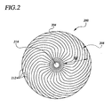
- FIG. 2 is a plan view of a polishing pad of the present invention suitable for use with the CMP system of FIG. 1;
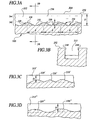
- FIG. 3A is an enlarged cross-sectional view of the polishing pad of FIG. 2 as taken along the longitudinal centerline of one of the grooves showing a plurality of mixing structures arranged within the groove
- FIG. 3B is a cross-sectional view of the polishing pad of FIG. 2 as taken along line 3B-3B of FIG. 3A
- FIG. 3C is an enlarged longitudinal cross-sectional view of the groove wherein the groove includes a plurality of alternative mixing structures arranged within the groove
- FIG. 3D is an enlarged longitudinal cross-sectional view of the groove wherein the groove includes a plurality of mixing structures and a nominal depth that varies linearly along the length of the groove;
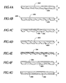
- FIGS. 4A-4G are perspective views of polishing pad grooves of the present invention illustrating various alternative mixing structures.
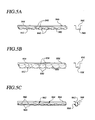
- FIGS. 5A-5C are perspective and corresponding cross-sectional views of polishing pad grooves of the present invention illustrating various more complex mixing structures.
- FIG. 1 shows in accordance with the present invention a chemical mechanical polishing (CMP) system, which is generally denoted by the numeral 100.
- CMP system 100 includes a polishing pad 104 having a polishing layer 108 that includes a plurality of grooves 112 configured for enhancing the utilization of a slurry 116, or other liquid polishing medium, applied to the polishing pad during polishing of a semiconductor substrate, such as semiconductor wafer 120 or other workpiece, such as glass, silicon wafer and magnetic information storage disk, among others.
- a semiconductor substrate such as semiconductor wafer 120 or other workpiece, such as glass, silicon wafer and magnetic information storage disk, among others.
- wafer workpiece
- Polishing pad 104 and its unique features are described in detail below.
- CMP system 100 may include a polishing platen 124 rotatable about an axis 126 by a platen driver 128.
- Platen 124 may have an upper surface 132 on which polishing pad 104 is mounted.
- a wafer carrier 136 rotatable about an axis 140 may be supported above polishing layer 108.
- Wafer carrier 136 may have a lower surface 144 that engages wafer 120.
- Wafer 120 has a surface 148 that faces polishing layer 108 and is planarized during polishing.
- Wafer carrier 136 may be supported by a carrier support assembly 152 adapted to rotate wafer 120 and provide a downward force F to press wafer surface 148 against polishing layer 108 so that a desired pressure exists between the wafer surface and the polishing layer during polishing.
- CMP system 100 may also include a slurry supply system 156 for supplying slurry 116 to polishing layer 108.
- Slurry supply system 156 may include a reservoir 160, e.g., a temperature controlled reservoir that holds slurry 116.
- a conduit 164 may carry slurry 116 from reservoir 160 to a location adjacent polishing pad 104 where the slurry is dispensed onto polishing layer 108.
- a flow control valve 168 may be used to control the dispensing of slurry 116 onto polishing pad 104.
- CMP system 100 may be provided with a system controller 172 for controlling the various components of the system, such as flow control valve 168 of slurry supply system 156, platen driver 128 and carrier support assembly 152, among others, during loading, polishing and unloading operations.
- system controller 172 includes a processor 176, memory 180 connected to the processor and support circuitry 184 for supporting the operation of the processor, memory and other components of the system controller.
- system controller 172 causes platen 124 and polishing pad 104 to rotate and activates slurry supply system 156 to dispense slurry 116 onto the rotating polishing pad. The slurry spreads out over polishing layer 108, including the gap beneath wafer 120 and polishing pad 104.
- System controller 172 also causes wafer carrier 136 to rotate at a selected speed, e.g., 0 rpm to 150 rpm, so that wafer surface 148 moves relative to the polishing layer 108.
- System controller 172 also controls wafer carrier 136 to provide a downward force F so as to induce a desired pressure, e.g., 0 psi to 15 psi, between wafer 120 and polishing pad 104.
- System controller 172 further controls the rotational speed of polishing platen 124, which is typically rotated at a speed of 0 to 150 rpm.
- FIG. 2 shows an exemplary polishing pad 200 that may be used as polishing pad 104 of FIG. 1 or with other polishing systems utilizing similar pads.
- Polishing pad 200 includes a polishing layer 204 that contains a polishing region 208, which confronts the surface of a wafer (not shown) during polishing.
- polishing pad 200 is designed for use in CMP system 100 of FIG. 1, wherein wafer 120 is rotated in a fixed position relative to platen 124, which itself rotates.
- polishing region 208 is annular in shape and has a width W equal to the diameter of the corresponding wafer, e.g., wafer 120 of FIG. 1.
- polishing region 208 would likewise be annular, but width W would be greater than the diameter of the wafer to account for the oscillation envelope. In other embodiments, polishing region 208 may extend across entire polishing layer 204.
- Polishing layer 204 includes a plurality of grooves 212 for enhancing the distribution and flow of slurry (not shown) throughout polishing region 208, among other reasons, such as to increase slurry retention time within the polishing region.
- grooves 212 are generally curved in shape and may be said to generally radiate outward from a central portion 216 of polishing layer.
- grooves 212 are shown thusly, those skilled in the art will readily appreciate that the underlying concepts of the present invention may be used with grooves defining any shape and pattern within polishing layer 204.
- grooves 212 may be any one of the other shapes discussed above in the background section, i.e., the radial, circular, Cartesian grid and spiral, to name a few.
- Polishing pad 200 may be of any conventional or other type construction.
- polishing pad 200 may be made of a microporous polyurethane, among other materials, and optionally include a compliant or rigid backing (not shown) to provide the proper support for the pad during polishing.
- Grooves 212 may be formed in polishing pad 200 using any process suitable for the material used to make the pad. For example, grooves 212 may be molded into polishing pad 200 or cut into the pad after the pad has been formed, among other ways. Those skilled in the art will understand how polishing pad 200 may be manufactured in accordance with the present invention.
- FIG. 3A shows a longitudinal cross-sectional view through one of grooves 212 of polishing pad 200 of FIG. 2.
- Groove 212 includes a plurality of mixing structures 220 (indicated generally by additional hatching) located along the length of the groove so as to defining the bottom 224 of the groove.
- mixing structures 220 define a series of peaks 228 (or, as mentioned below, plateaus) and valleys 232 that disturb the flow of slurry 236 in a lower portion 240 of the groove by an amount sufficient to inhibit the stratification of this flow.
- this disturbance causes some measure of mixing between slurry 236 in an upper portion 244 of groove 212 and the slurry in lower portion 240 of the groove.
- groove 212 includes spaced apart walls 248, which may be perpendicular to surface 252 of polishing layer as shown or, alternatively, may form an angle other than 90° with the surface. Also, as shown in FIG. 3B, groove 212 may have a bottom that is substantially parallel to surface 252 or, alternatively, may form a nonzero angle with the surface.
- mixing structures 220 may be defined relative to a nominal depth D of groove 212.
- Nominal depth D is the vertical distance between surface 252 of polishing layer 208 and a line obtained by connecting the lowest point on each valley 232 to the lowest point on each immediately adjacent valley.
- nominal depth D is uniform along the length of groove 212.
- nominal depth D of groove 212' may vary, depending upon the configurations of mixing structures 220' used.
- 3D illustrates how nominal depth D can vary linearly along the length of groove 212" in the presence of a plurality of uniformly sized and pitched mixing structures 220".
- nominal depth D may vary depending upon the selection and use of variously sized and shaped mixing structures.
- Mixing structures e.g., mixing structures 220 of FIG. 3A
- These ranges vary with the shapes of mixing structures 220 and the resulting valleys 232. Since there are many possible shapes, it is not practical to provide exact ranges, but rather general design principals.
- height H of mixing structures 220 must be great enough to effect at least some mixing, but not great enough that valleys 232 are so deep that flow separates and stagnates there.
- Pitch P of mixing structures 220 must be large enough that valleys 232 experience flow, but small enough that mixing of fresh and used slurry is not trivial and occurs along a significant length of groove 212.
- height H and pitch P of mixing structures 220 expected to result in good mixing capability are 10% to 50% of nominal depth D for height and one to four times nominal depth D for pitch P and preferably 15% to 30% of nominal depth D for height.
- mixing structures 220 are shown as being periodic and identical to one another, this need not be so. Rather, pitch P, height H, shape, or any combination of these, of mixing structures 220 may vary. Furthermore, while mixing structures 220 will typically be provided along the entire length of groove 212, they may be provided in one or more specific regions wherein mixing of slurry 236 is most desired. For example, mixing structures 220 may be present only in polishing region 208 of polishing layer 204. Similarly, although all grooves 212 on polishing pad 200 may be provided with mixing structures 220, this need not be so. If desired, only certain ones of grooves 212 of polishing pad 200 of FIG. 2, may be provided with mixing structures 220. For example, relative to grooves 212 of FIG. 2, every other groove or every third groove may not be provided with mixing structures 220, among other possibilities.
- FIGS. 4A-4G show a sample of alternative shapes that may be used for mixing structures within the grooves of polishing pads, e.g., polishing pads 104, 200 of FIGS. 1 and 2, respectively.
- each mixing structure 300 is triangular so as to form generally V-shaped valleys 304.
- FIG. 4B shows each mixing structure 400 as being skew-sawtooth-shaped so as to impart a pattern of unequal ascending and descending slopes to bottom 404 of groove 408.
- FIG. 4C shows hill-shaped mixing structures 500, 520 having two heights that alternate with one another.
- Mixing structures 600 of FIG. 4D are shaped so as to define scallop-shaped valleys 604.
- Mixing structures 700 of FIG. 4E each have an arch-shaped upper surface 704.
- Mixing structures 800 of FIG. 4F are generally trapezoidal in shape so as to define plateaus 804.
- FIG. 4G shows mixing structures 900 having shapes that are somewhat random among the mixing structures.
- FIGS. 5A-5C show a sample of additional alternative shapes that may be used for mixing structures within the grooves of a polishing pad of the present invention, e.g. grooves 112, 212 of polishing pads of FIGS. 1 and 2, respectively, in particular mixing structures having a height H that varies not only with distance along the groove, but also with distance across the groove.
- FIG. 5A shows mixing structures 940 that result when two identical geometries 942, 944 (where the sides of groove 946 meet the bottom of the groove) are shifted relative to one another along the length of the groove and connected by straight lines 948 at their corresponding points.
- FIG. 1 shows mixing structures 940 that result when two identical geometries 942, 944 (where the sides of groove 946 meet the bottom of the groove) are shifted relative to one another along the length of the groove and connected by straight lines 948 at their corresponding points.
- FIG. 5B shows mixing structures 950 that result when two identical geometries 952, 954 are shifted relative to one another along the depth of groove 956 and connected by straight lines 958 at their corresponding points.
- FIG. 5C shows mixing structures 960 formed as two distinct sets 962, 964 of structures occupying opposites sides of groove 966 such that, in general, the cross-sectional shape of the groove has a discontinuity in height.
Landscapes
- Engineering & Computer Science (AREA)
- Mechanical Engineering (AREA)
- Mechanical Treatment Of Semiconductor (AREA)
- Finish Polishing, Edge Sharpening, And Grinding By Specific Grinding Devices (AREA)
- Grinding-Machine Dressing And Accessory Apparatuses (AREA)
Applications Claiming Priority (2)
| Application Number | Priority Date | Filing Date | Title |
|---|---|---|---|
| US10/712,186 US7018274B2 (en) | 2003-11-13 | 2003-11-13 | Polishing pad having slurry utilization enhancing grooves |
| US712186 | 2003-11-13 |
Publications (2)
| Publication Number | Publication Date |
|---|---|
| EP1533075A1 EP1533075A1 (en) | 2005-05-25 |
| EP1533075B1 true EP1533075B1 (en) | 2007-07-18 |
Family
ID=34435661
Family Applications (1)
| Application Number | Title | Priority Date | Filing Date |
|---|---|---|---|
| EP04256800A Expired - Lifetime EP1533075B1 (en) | 2003-11-13 | 2004-11-04 | Polishing pad having slurry utilization enhancing grooves |
Country Status (7)
| Country | Link |
|---|---|
| US (1) | US7018274B2 (enExample) |
| EP (1) | EP1533075B1 (enExample) |
| JP (1) | JP4689241B2 (enExample) |
| KR (1) | KR101157649B1 (enExample) |
| CN (1) | CN100343958C (enExample) |
| DE (1) | DE602004007597T2 (enExample) |
| TW (1) | TWI339146B (enExample) |
Families Citing this family (19)
| Publication number | Priority date | Publication date | Assignee | Title |
|---|---|---|---|---|
| US7377840B2 (en) * | 2004-07-21 | 2008-05-27 | Neopad Technologies Corporation | Methods for producing in-situ grooves in chemical mechanical planarization (CMP) pads, and novel CMP pad designs |
| WO2005030439A1 (ja) * | 2003-09-26 | 2005-04-07 | Shin-Etsu Handotai Co., Ltd. | 研磨布及び研磨布の加工方法並びにそれを用いた基板の製造方法 |
| US6958002B1 (en) * | 2004-07-19 | 2005-10-25 | Rohm And Haas Electronic Materials Cmp Holdings, Inc. | Polishing pad with flow modifying groove network |
| KR101334012B1 (ko) * | 2005-07-25 | 2013-12-02 | 호야 가부시키가이샤 | 마스크 블랭크용 기판의 제조방법, 마스크 블랭크의제조방법 및 마스크의 제조방법 |
| JP5080769B2 (ja) * | 2006-09-15 | 2012-11-21 | 株式会社東京精密 | 研磨方法及び研磨装置 |
| US9180570B2 (en) | 2008-03-14 | 2015-11-10 | Nexplanar Corporation | Grooved CMP pad |
| CN102814725B (zh) * | 2011-06-08 | 2015-11-25 | 无锡华润上华科技有限公司 | 一种化学机械研磨方法 |
| JP6065208B2 (ja) * | 2012-12-25 | 2017-01-25 | 富士紡ホールディングス株式会社 | 研磨パッド及びその製造方法 |
| JP5919592B1 (ja) * | 2015-02-23 | 2016-05-18 | 防衛装備庁長官 | 研磨装置 |
| US9770092B2 (en) * | 2015-08-20 | 2017-09-26 | Taiwan Semiconductor Manufacturing Co., Ltd. | Brush, back surface treatment assembly and method for cleaning substrate |
| CN105500183B (zh) * | 2015-11-26 | 2018-08-10 | 上海集成电路研发中心有限公司 | 一种研磨垫及其使用周期检测方法 |
| SE539716C2 (en) * | 2016-06-15 | 2017-11-07 | Valmet Oy | Refine plate segment with pre-dam |
| US10688621B2 (en) * | 2016-08-04 | 2020-06-23 | Rohm And Haas Electronic Materials Cmp Holdings, Inc. | Low-defect-porous polishing pad |
| KR102702996B1 (ko) * | 2018-12-10 | 2024-09-04 | 삼성전자주식회사 | 연마 균일도를 제어할 수 있는 화학 기계적 연마 장치 |
| GB2582639B (en) * | 2019-03-29 | 2023-10-18 | Zeeko Innovations Ltd | Shaping apparatus, method and tool |
| CN113021181B (zh) * | 2021-03-22 | 2023-05-30 | 万华化学集团电子材料有限公司 | 一种高去除速率、低划伤化学机械抛光垫及其应用 |
| CN114619362B (zh) * | 2022-04-07 | 2024-04-12 | 南京理工大学 | 一种球阀研磨盘装置 |
| CN115922557B (zh) * | 2023-03-09 | 2023-07-25 | 长鑫存储技术有限公司 | 一种抛光组件及抛光设备 |
| DE102024109581A1 (de) * | 2024-04-05 | 2025-10-09 | Lapmaster Wolters Gmbh | Läppscheibe für eine Läppmaschine, Läppmaschine und Verfahren zum Läppen eines Werkstücks mit einer Läppmaschine |
Family Cites Families (19)
| Publication number | Priority date | Publication date | Assignee | Title |
|---|---|---|---|---|
| AT374206B (de) * | 1982-11-15 | 1984-03-26 | Hirsch Kurt | Verfahren und vorrichtung zum vorschaeumen von kunststoffen |
| US5093651A (en) * | 1990-10-11 | 1992-03-03 | Thomas Edward M | Intelligent smoke detector |
| JP3042593B2 (ja) * | 1995-10-25 | 2000-05-15 | 日本電気株式会社 | 研磨パッド |
| US5645469A (en) * | 1996-09-06 | 1997-07-08 | Advanced Micro Devices, Inc. | Polishing pad with radially extending tapered channels |
| US6273806B1 (en) * | 1997-05-15 | 2001-08-14 | Applied Materials, Inc. | Polishing pad having a grooved pattern for use in a chemical mechanical polishing apparatus |
| US5921855A (en) | 1997-05-15 | 1999-07-13 | Applied Materials, Inc. | Polishing pad having a grooved pattern for use in a chemical mechanical polishing system |
| US6093651A (en) | 1997-12-23 | 2000-07-25 | Intel Corporation | Polish pad with non-uniform groove depth to improve wafer polish rate uniformity |
| US6139402A (en) * | 1997-12-30 | 2000-10-31 | Micron Technology, Inc. | Method and apparatus for mechanical and chemical-mechanical planarization of microelectronic substrates |
| JPH11216663A (ja) * | 1998-02-03 | 1999-08-10 | Sony Corp | 研磨パッド、研磨装置および研磨方法 |
| JPH11267961A (ja) * | 1998-03-23 | 1999-10-05 | Sony Corp | 研磨パッド、研磨装置および研磨方法 |
| JP2000033553A (ja) * | 1998-05-11 | 2000-02-02 | Sony Corp | 研磨パッドおよび研磨方法 |
| JP2000000755A (ja) * | 1998-06-16 | 2000-01-07 | Sony Corp | 研磨パッド及び研磨方法 |
| KR20000025003A (ko) * | 1998-10-07 | 2000-05-06 | 윤종용 | 반도체 기판의 화학 기계적 연마에 사용되는 연마 패드 |
| US6110832A (en) * | 1999-04-28 | 2000-08-29 | International Business Machines Corporation | Method and apparatus for slurry polishing |
| US20020068516A1 (en) | 1999-12-13 | 2002-06-06 | Applied Materials, Inc | Apparatus and method for controlled delivery of slurry to a region of a polishing device |
| US6241596B1 (en) * | 2000-01-14 | 2001-06-05 | Applied Materials, Inc. | Method and apparatus for chemical mechanical polishing using a patterned pad |
| US6656019B1 (en) * | 2000-06-29 | 2003-12-02 | International Business Machines Corporation | Grooved polishing pads and methods of use |
| KR20030015567A (ko) * | 2001-08-16 | 2003-02-25 | 에스케이에버텍 주식회사 | 웨이브 형태의 그루브가 형성된 화학적 기계적 연마패드 |
| US6602123B1 (en) * | 2002-09-13 | 2003-08-05 | Infineon Technologies Ag | Finishing pad design for multidirectional use |
-
2003
- 2003-11-13 US US10/712,186 patent/US7018274B2/en not_active Expired - Lifetime
-
2004
- 2004-11-01 TW TW093133219A patent/TWI339146B/zh not_active IP Right Cessation
- 2004-11-04 DE DE602004007597T patent/DE602004007597T2/de not_active Expired - Lifetime
- 2004-11-04 EP EP04256800A patent/EP1533075B1/en not_active Expired - Lifetime
- 2004-11-12 KR KR1020040092276A patent/KR101157649B1/ko not_active Expired - Lifetime
- 2004-11-12 CN CNB2004100929813A patent/CN100343958C/zh not_active Expired - Lifetime
- 2004-11-15 JP JP2004330015A patent/JP4689241B2/ja not_active Expired - Lifetime
Also Published As
| Publication number | Publication date |
|---|---|
| DE602004007597T2 (de) | 2008-04-17 |
| DE602004007597D1 (de) | 2007-08-30 |
| TW200529978A (en) | 2005-09-16 |
| JP2005150745A (ja) | 2005-06-09 |
| CN1617308A (zh) | 2005-05-18 |
| US20050107009A1 (en) | 2005-05-19 |
| KR101157649B1 (ko) | 2012-06-18 |
| KR20050046599A (ko) | 2005-05-18 |
| JP4689241B2 (ja) | 2011-05-25 |
| EP1533075A1 (en) | 2005-05-25 |
| US7018274B2 (en) | 2006-03-28 |
| CN100343958C (zh) | 2007-10-17 |
| TWI339146B (en) | 2011-03-21 |
Similar Documents
| Publication | Publication Date | Title |
|---|---|---|
| EP1533075B1 (en) | Polishing pad having slurry utilization enhancing grooves | |
| US7125318B2 (en) | Polishing pad having a groove arrangement for reducing slurry consumption | |
| US7059949B1 (en) | CMP pad having an overlapping stepped groove arrangement | |
| US7059950B1 (en) | CMP polishing pad having grooves arranged to improve polishing medium utilization | |
| KR101107636B1 (ko) | 프로세스 의존성 홈 구조를 갖는 화학 기계식 연마 패드 | |
| US8062103B2 (en) | High-rate groove pattern | |
| US9308620B2 (en) | Permeated grooving in CMP polishing pads | |
| JP4820555B2 (ja) | 溝付き研磨パッド及び方法 | |
| EP2202031A2 (en) | High-rate polishing method | |
| US6974372B1 (en) | Polishing pad having grooves configured to promote mixing wakes during polishing | |
| US6958002B1 (en) | Polishing pad with flow modifying groove network | |
| US7520796B2 (en) | Polishing pad with grooves to reduce slurry consumption |
Legal Events
| Date | Code | Title | Description |
|---|---|---|---|
| PUAI | Public reference made under article 153(3) epc to a published international application that has entered the european phase |
Free format text: ORIGINAL CODE: 0009012 |
|
| 17P | Request for examination filed |
Effective date: 20041117 |
|
| AK | Designated contracting states |
Kind code of ref document: A1 Designated state(s): AT BE BG CH CY CZ DE DK EE ES FI FR GB GR HU IE IS IT LI LU MC NL PL PT RO SE SI SK TR |
|
| AX | Request for extension of the european patent |
Extension state: AL HR LT LV MK YU |
|
| AKX | Designation fees paid |
Designated state(s): DE FR GB IT |
|
| RAP1 | Party data changed (applicant data changed or rights of an application transferred) |
Owner name: ROHM AND HAAS ELECTRONIC MATERIALS CMP HOLDINGS, I |
|
| GRAP | Despatch of communication of intention to grant a patent |
Free format text: ORIGINAL CODE: EPIDOSNIGR1 |
|
| GRAS | Grant fee paid |
Free format text: ORIGINAL CODE: EPIDOSNIGR3 |
|
| GRAA | (expected) grant |
Free format text: ORIGINAL CODE: 0009210 |
|
| AK | Designated contracting states |
Kind code of ref document: B1 Designated state(s): DE FR GB IT |
|
| REG | Reference to a national code |
Ref country code: GB Ref legal event code: FG4D |
|
| REF | Corresponds to: |
Ref document number: 602004007597 Country of ref document: DE Date of ref document: 20070830 Kind code of ref document: P |
|
| ET | Fr: translation filed | ||
| PLBE | No opposition filed within time limit |
Free format text: ORIGINAL CODE: 0009261 |
|
| STAA | Information on the status of an ep patent application or granted ep patent |
Free format text: STATUS: NO OPPOSITION FILED WITHIN TIME LIMIT |
|
| 26N | No opposition filed |
Effective date: 20080421 |
|
| GBPC | Gb: european patent ceased through non-payment of renewal fee |
Effective date: 20081104 |
|
| PG25 | Lapsed in a contracting state [announced via postgrant information from national office to epo] |
Ref country code: GB Free format text: LAPSE BECAUSE OF NON-PAYMENT OF DUE FEES Effective date: 20081104 |
|
| PG25 | Lapsed in a contracting state [announced via postgrant information from national office to epo] |
Ref country code: IT Free format text: LAPSE BECAUSE OF NON-PAYMENT OF DUE FEES Effective date: 20071130 |
|
| REG | Reference to a national code |
Ref country code: FR Ref legal event code: PLFP Year of fee payment: 12 |
|
| REG | Reference to a national code |
Ref country code: FR Ref legal event code: PLFP Year of fee payment: 13 |
|
| REG | Reference to a national code |
Ref country code: FR Ref legal event code: PLFP Year of fee payment: 14 |
|
| REG | Reference to a national code |
Ref country code: FR Ref legal event code: PLFP Year of fee payment: 15 |
|
| PGFP | Annual fee paid to national office [announced via postgrant information from national office to epo] |
Ref country code: FR Payment date: 20221010 Year of fee payment: 19 |
|
| PGFP | Annual fee paid to national office [announced via postgrant information from national office to epo] |
Ref country code: DE Payment date: 20220621 Year of fee payment: 19 |
|
| REG | Reference to a national code |
Ref country code: DE Ref legal event code: R119 Ref document number: 602004007597 Country of ref document: DE |
|
| PG25 | Lapsed in a contracting state [announced via postgrant information from national office to epo] |
Ref country code: DE Free format text: LAPSE BECAUSE OF NON-PAYMENT OF DUE FEES Effective date: 20240601 |
|
| PG25 | Lapsed in a contracting state [announced via postgrant information from national office to epo] |
Ref country code: FR Free format text: LAPSE BECAUSE OF NON-PAYMENT OF DUE FEES Effective date: 20231130 |
|
| PG25 | Lapsed in a contracting state [announced via postgrant information from national office to epo] |
Ref country code: FR Free format text: LAPSE BECAUSE OF NON-PAYMENT OF DUE FEES Effective date: 20231130 Ref country code: DE Free format text: LAPSE BECAUSE OF NON-PAYMENT OF DUE FEES Effective date: 20240601 |