EP1532197B1 - Verfahren zum schweissen einer polymeren oberfläche mit einer elektrisch leitenden oder halbleitendem oberfläche - Google Patents
Verfahren zum schweissen einer polymeren oberfläche mit einer elektrisch leitenden oder halbleitendem oberfläche Download PDFInfo
- Publication number
- EP1532197B1 EP1532197B1 EP03773828A EP03773828A EP1532197B1 EP 1532197 B1 EP1532197 B1 EP 1532197B1 EP 03773828 A EP03773828 A EP 03773828A EP 03773828 A EP03773828 A EP 03773828A EP 1532197 B1 EP1532197 B1 EP 1532197B1
- Authority
- EP
- European Patent Office
- Prior art keywords
- polymer
- film
- conductive
- semiconductive
- organic film
- Prior art date
- Legal status (The legal status is an assumption and is not a legal conclusion. Google has not performed a legal analysis and makes no representation as to the accuracy of the status listed.)
- Expired - Lifetime
Links
Images
Classifications
-
- C—CHEMISTRY; METALLURGY
- C09—DYES; PAINTS; POLISHES; NATURAL RESINS; ADHESIVES; COMPOSITIONS NOT OTHERWISE PROVIDED FOR; APPLICATIONS OF MATERIALS NOT OTHERWISE PROVIDED FOR
- C09D—COATING COMPOSITIONS, e.g. PAINTS, VARNISHES OR LACQUERS; FILLING PASTES; CHEMICAL PAINT OR INK REMOVERS; INKS; CORRECTING FLUIDS; WOODSTAINS; PASTES OR SOLIDS FOR COLOURING OR PRINTING; USE OF MATERIALS THEREFOR
- C09D5/00—Coating compositions, e.g. paints, varnishes or lacquers, characterised by their physical nature or the effects produced; Filling pastes
- C09D5/44—Coating compositions, e.g. paints, varnishes or lacquers, characterised by their physical nature or the effects produced; Filling pastes for electrophoretic applications
- C09D5/4476—Coating compositions, e.g. paints, varnishes or lacquers, characterised by their physical nature or the effects produced; Filling pastes for electrophoretic applications comprising polymerisation in situ
-
- C—CHEMISTRY; METALLURGY
- C08—ORGANIC MACROMOLECULAR COMPOUNDS; THEIR PREPARATION OR CHEMICAL WORKING-UP; COMPOSITIONS BASED THEREON
- C08J—WORKING-UP; GENERAL PROCESSES OF COMPOUNDING; AFTER-TREATMENT NOT COVERED BY SUBCLASSES C08B, C08C, C08F, C08G or C08H
- C08J5/00—Manufacture of articles or shaped materials containing macromolecular substances
- C08J5/12—Bonding of a preformed macromolecular material to the same or other solid material such as metal, glass, leather, e.g. using adhesives
- C08J5/121—Bonding of a preformed macromolecular material to the same or other solid material such as metal, glass, leather, e.g. using adhesives by heating
-
- C—CHEMISTRY; METALLURGY
- C08—ORGANIC MACROMOLECULAR COMPOUNDS; THEIR PREPARATION OR CHEMICAL WORKING-UP; COMPOSITIONS BASED THEREON
- C08J—WORKING-UP; GENERAL PROCESSES OF COMPOUNDING; AFTER-TREATMENT NOT COVERED BY SUBCLASSES C08B, C08C, C08F, C08G or C08H
- C08J5/00—Manufacture of articles or shaped materials containing macromolecular substances
- C08J5/12—Bonding of a preformed macromolecular material to the same or other solid material such as metal, glass, leather, e.g. using adhesives
- C08J5/122—Bonding of a preformed macromolecular material to the same or other solid material such as metal, glass, leather, e.g. using adhesives using low molecular chemically inert solvents, swelling or softening agents
Definitions
- the present invention relates to a method for welding a polymer surface with a conductive or semiconductive surface, to the applications of this method as well as structures obtained by its implementation.
- Polymeric surface means a surface consisting of a polymer and corresponding to all or part of the surface of an object which may be composed exclusively of that polymer or formed of one or more other materials and at least a part of the surface is made of said polymer.
- the object may be an object comprising a conductive or semiconductive area of electricity and whose surface is made of a polymer.
- Conductive or semiconducting surface means a surface made of a conductive or semi-conducting material of electricity and corresponding to all or part of the surface of an object which may be exclusively composed of conducting or semiconductor material is formed of one or more other materials and at least a part of the surface of which is made of said conductive or semiconductor material.
- the method according to the invention is obviously capable of finding an application in all areas where it is necessary to secure a polymer, and in particular a thermofusible polymer, with a conductive surface or semiconductor electricity.
- the process according to the invention may make it possible, for example, to remedy the problems of peeling of paints and coatings to protect parts against corrosion.
- the biomedical field where the method according to the invention may be useful, for example, for covering implantable medical or surgical equipment such as stents, aneurysm guides, catheter guides, cardiac pacemakers, hip prostheses, cochlear implant electrodes, dental implants or electrophysiology electrodes, with biocompatible materials capable of providing controlled release of biologically active substances.
- the method according to the invention can also find application in the fields where it is necessary to achieve a solid mechanical fixation between two objects having conductive or semiconducting areas of electricity, and in particular when the fixing has to be carried out. at these areas.
- the method which is the subject of the invention can be very useful in the case where it is desirable for the attachment to be at temperatures lower than those required for direct thermal welding, whether for technical reasons (such as the sensitivity of the materials to heat) or economic, or when the attachment is intended to be done via a flexible connection.
- Such constraints are very present in the assembly of sensitive elements constituting micro-systems such as micro-sensors, and in particular in the assembly carried out by the so-called technology of "connectivity by polymer ball" still known in the English terminology. -signs "polymer flip chip” (PFC).
- organic materials have localized surface states: in chemical terms, they are said to have functional groups.
- to make chemistry on a polymer surface is "simple" insofar as it involves reacting functional groups together and, therefore, to take advantage of the experience acquired in organic chemistry.
- the surface of conductive or semi-conducting materials is made of delocalized electronic states (apart from surface defects): in chemical terms, the very notion of functional groupings disappears and we do not can further apply to the surface chemistry of conductive or semiconductor materials the experience gained in organic chemistry.
- complementary functional groups such as isocyanate groups ( EP-A-1 110 946 [1] ), siloxanes ( WO-A-00/51732 [2] ) or acid chlorides ( FR-A-2,781,232 [3] ), or by using bi-functional coupling agents or else primary chemical adhesion agents such as ⁇ -
- US Patent 6,022,597 [5] proposes to expose the surface to a reagent having nitrogen generating groups (azide groups for example) and to bombard this surface with particles (ions, electrons, protons, etc.) to transform the generating groups.
- nitrogen in nitrene groups capable of subsequently reacting with a large number of organic functional groups.
- the patent U.S. Patent No. 6,287,687 [6] proposes to functionalize a surface by applying a plasma treatment in which the plasma gas contains a monomer capable of polymerizing or co-polymerizing with other polymerizable compounds under the effect of irradiation.
- the patent U.S. 4,421,569 [7] provides for the functionalization of a surface by applying an aqueous suspension comprising a precursor monomer of a polymer, a prepolymer, metal salts and a catalyst, the metal salts for oxidizing said surface so as to create therein radicals capable of initiating the polymerization reactions of the monomer and the prepolymer.
- the surface of the conductive or semiconductor material can be further functionalized via radicals which are reacted by irradiation with heavy ions ( US Patent 6,306,975 [8] ), thermally ( WO-A-98/49206 [9] ) or photochemically as described in WO-A-99/16907 [10].
- Another type of solution consists, no longer in creating chemical bonds at the organic material / conductive or semiconductor material interface, but in forming a layer of the organic material on the conductive or semiconducting surface. which is insoluble in most known solvents, based on the fact that the physical forces present are sufficient to guarantee the adhesion of this organic material to said surface, provided that the interface is stable.
- this deposit can be obtained in particular by crosslinking the organic material during or after its deposition on the surface of the conductive or semiconductive material, this deposit can be carried out by centrifugation or "spin-coating", or by dipping or “dip-coating".
- This pathway is used in the biomedical field, for example to cover stents with polymeric reservoirs of active molecules, which are then stabilized by fibrin crosslinking ( EP-A-0 701 802 [11] ) or a chemical crosslinking agent ( WO-A-98/32474 [12] ), as well as in the field of micro-systems for making polymer pads for the mechanical assembly of micro-structures by PFC technology, or for the encapsulation of micro-systems ( US Patent 6,335,571 [13] ).
- the term "electrografting" of an organic film on a conductive or semiconductive surface an operation which consists in putting this surface in contact with at least one precursor of this organic film and to induce, by application to the conductive or semiconducting surface of one or more electrical potential sweeps, the covalent bonding of this precursor to said surface and thereby the formation of an organic film.
- the attachment of the precursor on the conductive or semiconducting surface may, when the latter is suitable, be accompanied by polymerization reactions of said precursor which in particular have the effect of increasing the thickness of said organic film.
- welding operation of a polymer surface with a conductive or semiconductive surface, an operation which consists in joining these two surfaces so that they form an undivided mass.
- this operation can also be performed cold, for example by means of a substance capable of dissolving or swelling the polymer surface and the organic electrografted film on the conductive or semiconductive surface - this type of operation being referred to in what follows by the term "gluing" - that hot, that is to say by a supply of thermal energy to cause melting of the surfaces in the presence - this type of operation being hereinafter called “thermofusion”, or even combining a bonding and a thermofusion.
- the method according to the invention makes it possible to subject the conductive or semiconductive surface to pretreatment, which consists of electrografting of an organic film, the film thus electrografted having the double advantage of being very adherent to the surface that gave birth to it, and to be organic as the polymer surface to be secured to the conductive or semiconductive surface.
- this film is generally low to very low (that is to say less than 1 ⁇ m, or even 500 nm), it turns out that, surprisingly, it is suitable for serve as a "germ” of welding and to allow the realization of a weld between the conductive or semi-conductive surface and a polymer surface, by simple contact of the latter and application of welding conditions.
- the electrografting of the organic film on the conductive or semiconductive surface may be electro-initiated grafting or electro-tracking deposition, in which case the organic film is a polymer film.
- electro-tracking deposit While, in the case of an electro-tracking deposit, the polymerization reactions of the precursor are electro-chemical as the attachment of this precursor on the conductive or semiconducting surface, and therefore remain related to maintaining a potential electric.
- electro-tracking deposit is the electropolymerization which uses as precursors, conductive monomers such as pyrrole, aniline, thiophene or EDOT (Ethylene Di-Oxy Thiophene).
- the electrografting of the organic polymer film be an electro-initiated grafting
- the inventors having, in fact, found that this type of electrografting has the advantage: (i ) leading to the formation of covalent bonds between the polymeric organic film and the conductive or semiconductive surface; (ii) allowing extreme localization of the polymer deposit on selected areas having a given output work; (iii) to allow a very precise control on the homogeneity of thickness, even on topographies of ohmic falls very rough (rough surfaces, worked surfaces comprising reasons with high ratio of aspect, ).
- the organic film being a polymer film
- the precursor is a precursor monomer or prepolymer of this film or a mixture of both.
- the electrografting of the polymer film comprises, in addition to the attachment of the precursor of this film to the conductive or semiconductive surface, polymerization chain reactions of this precursor. These polymerization reactions are carried out from the monomers and / or prepolymers which have clung to said surface under the effect of the electric potential, and results in a growth or "push" of polymer chains from this surface. Each polymer chain thus formed is thus covalently bonded to the conductive or semiconductive surface.
- the precursor monomers and prepolymers of the organic film may be chosen, in the first place, from organic compounds comprising vinyl groups, in which case the electro-initiation consists of an electro-reduction (or an electro-reduction). -oxidation), these monomers and / or prepolymers, and it is the monomers and / or prepolymers thus electro-reduced (or electro-oxidized) that initiate the polymerization reactions, which are, in this case, anionic (or cationic) .
- vinyl monomers such as acrylonitrile, methacrylonitrile, acrylates and methacrylates (acrylate and methyl methacrylate, acrylate and methacrylate) propyl acrylate and methacrylate, butyl acrylate and methacrylate, hydroxyethyl acrylate and methacrylates, glycidyl acrylate and methacrylate, polyethylene glycol dimethacrylate, polydimethylsiloxane acrylate and methacrylate), acrylamides and methacrylamides, cyanoacrylates, acrylic acid and methacrylic acid, styrene, vinyl halides, N-vinyl pyrrolidone, 2-vinyl pyridine, 4-vinyl pyridine and telechelic compounds with vinyl ends.
- vinyl monomers such as acrylonitrile, methacrylonitrile, acrylates and methacrylates (acrylate and methyl methacrylate, acrylate and methacrylate) propyl
- the monomers and prepolymers may also be chosen from organic compounds comprising cleavable cyclic groups by a nucleophilic or electrophilic attack, in which case the electrografting is carried out according to the same principle as the previous one, apart from the fact that the growth of the polymer chains results from the opening of the cycles of the monomers or prepolymers.
- the precursor of the organic film is chosen from diazonium salts, in particular aryl diazonium salts, sulphonium, phosphonium and iodonium salts, and their salts. mixtures, these salts being preferably functionalized by macromolecular fragments of polyethylene type and other polyolefins, polyethylene oxide, and more generally any oligomer or hot melt polymer.
- the electrografting of the organic film is preferably obtained by immersing the conductive or semiconductive surface in a solution containing the precursor (s) of said organic film and by connecting this surface to a potentiostat of in order to apply to it one or more electrical potential scans, these scans being continuous or discontinuous, sinusoidal or crenellated scans.
- the operation of welding the polymer surface with the conductive or semiconducting surface may be carried out, which operation preferably consists of a thermofusion or a collage or else in a thermofusion / bonding combination.
- the hot melt can be carried out by applying one surface to the other and supplying to the resulting assembly, possibly pressurized or under compression, a thermal energy, for example by heating or by application of electromagnetic radiation, sufficient to obtain the fusion of the two surfaces in the presence and, therefore, their interpenetration.
- Sufficient thermal energy corresponds, for example, to a temperature higher than that which, glass transition temperatures of the polymer surface to be welded and electro-grafted organic film on the conductive or semiconductive surface, is the highest.
- bonding agent preferably used as bonding agent is a substance, for example a solvent, which is capable of both dissolving or swelling the polymer surface to be welded and the electrografted organic film. on the conductive or semiconductive surface.
- the bonding may be carried out by coating the polymer surface and the conductive or semiconducting surface with bonding agent, then applying one surface on the other and drying the resulting assembly, optionally under reduced pressure and / or in press or under tightening.
- the polymer constituting the polymer surface to be welded may be purely organic or hybrid (that is to say organic-inorganic), hot-melt or thermoplastic provided that, in the latter case, it is capable of being solubilized or swollen by substance which is also a solvent or a swelling of the material forming the electrografted organic film.
- the electrografted organic film is itself a polymer film
- the polymer constituting the polymer surface to be welded can be both identical and different from the polymer constituting this organic film.
- Suitable polymers include polyethylenes, polypropylenes, polystyrenes, polyacrylonitriles, polysiloxanes, polyesters such as polylactic acid and polyglycolic acid, polyorthoesters, polycaprolactones, polybutyrolactones, polyacrylics, polymethacrylics, polyacrylamides , epoxy resins, ABS resins, polyvinyl chloride, polycarbonate, polytetrafluoroethylene and perfluorinated polyethers, phenoplast resins, polyurethanes, epoxy resins, their copolymers and their mixtures.
- thermosetting polymers are those which are preferred for use in the context of the present invention, even though thermosetting polymers may also be interesting candidates.
- the material likely to constitute the conductive or semiconducting surface it may be any material known to have conductive or semiconductive properties of electricity, such as metals (noble or not) and metal alloys, silicon, germanium or gallium arsenide.
- the process according to the invention has many advantages.
- first conductive or semiconductor material covered with an organic film, electrografted or not with a second conductive or semiconductive material which itself is not covered with a film organic.
- second conductive or semiconductive material which itself is not covered with a film organic.
- the welding operation can be performed after not only electro-grafting an organic film onto the surface of the second conductive or semiconductor material, but also inserting a polymer film between the organic films forming the surfaces of the two conductive or semiconductor materials.
- the organic film forming the surface of the first conductive or semiconductor material is an electrografted film, the electrografting making it possible to dispose of stronger interfaces than the other methods currently available to form an organic film on a surface.
- the method according to the invention makes it possible to weld together two conductive or semiconducting materials which are neither of them covered with a polymer film.
- the electrografted organic film on the conductive or semiconducting surface may or may not consist of the same polymer as that forming the polymer surface with which said conductive or semiconductive surface is intended to be soldered.
- the method according to the invention makes it possible very easily to obtain, on a conductive or semiconducting material, thick to very thick films, and in particular macroscopic films (i.e. more than 500 ⁇ m thick) and very adherent, whereas electrografting alone leads to the formation of films whose thickness does not exceed one micron.
- the films thus obtained may, for example, be plastic films made by extrusion or any other means, which is then welded to the conductive or semiconductor material. previously electro-grafted by a film of the same nature.
- the method according to the invention makes it possible to obtain, on a conductive or semiconductive surface, a polymer film which, normally, could not have been electrografted on this surface or with serious difficulties.
- electrografting is a complex process that does not allow the grafting of all polymers with the same efficiency on all conductive or semiconducting surfaces.
- certain polymers such as those obtained by polycondensation of monomers, do not lend themselves to electrografting.
- the method according to the invention offers a solution to this problem since it is sufficient to electro-graft, on the conductive or semiconductive surface, a polymer film that is both compatible with the one that was initially sought to be coated. this surface, and easy to electro-graft on said surface.
- the method according to the invention makes it possible to create very strong adhesion bonds between the welded surfaces.
- the subject of the invention is also a structure comprising two objects, one of which has a conductive or semi-conducting surface of electricity and the other of which comprises a polymer surface, these surfaces being welded to one another by intermediate of an organic film having a thickness of less than 1 ⁇ m which is electro-grafted onto said conductive or semiconductive surface of electricity.
- Also described is a structure comprising a conductive or semiconductive surface welded to a polymer surface via an organic film, wherein said organic film is bonded to said conductive or semiconductive surface by covalent bonds.
- Such structures are, for example, implantable medical or surgical devices such as stents, aneurysm guides, catheter guides, pacemakers, hip prostheses, cochlear implant electrodes, dental implants or electrophysiology electrodes, or micro-systems such as microphones -capteurs.
- implantable medical or surgical devices such as stents, aneurysm guides, catheter guides, pacemakers, hip prostheses, cochlear implant electrodes, dental implants or electrophysiology electrodes, or micro-systems such as microphones -capteurs.
- the invention also comprises other provisions which will emerge from the additional description which follows, which relates to embodiments of welds by the method according to the invention and their performance, and which is given for illustrative and non-limiting, with reference to the accompanying drawings.
- Example 1 Thermofusion welding of a gold wire on a gold blade
- butyl methacrylate (BuMA) is dissolved in a solution comprising 5 ⁇ 10 -2 mol / l of tetraethylammonium perchlorate in dimethyl formamide (DMF), at a concentration of 5 moles of butyl methacrylate. per liter of solution.
- DMF dimethyl formamide
- This solution is then immersed in a glass slide covered with an evaporated gold layer.
- This blade is connected to the working terminal of a potentiostat and serves as a working electrode.
- Both other electrodes of the device are a large platinum electrode, which serves as a counter-electrode, and a silver wire, used as a reference electrode.
- the wire is then deposited on the blade and held with a Mohr forceps. The whole is placed overnight in an oven heated to 200 ° C, which represents a temperature well below the melting temperature of gold (1064.43 ° C).
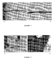
- the figure 1 represents two photographs taken under an optical microscope at zones where the thermofusion between the wire and the blade seems apparent, the photograph A corresponding to a magnification of 50x and photograph B corresponding to a magnification of 100x.
- a 316L stainless steel strip 10 cm long and 1 cm wide was dipped in a solution of 3.125 mol / l of methyl methacrylate (MMA), 10 -2 mol / l of 4-nitrophenyl diazonium tetrafluoroborate and 2.5 ⁇ 10 -2 mol / l of sodium nitrate in DMF.
- This blade serves as a working electrode in a three-electrode arrangement similar to that used in Example 1.
- This slide is subjected to a series of 50 potential sweeps under voltammetric conditions, between -0.1 and -3.0 V / (Ag + / Ag), at a speed of 100 mV / s.
- the slide is then rinsed with DMF, then with acetone, and finally dried under a stream of nitrogen.
- a polymethyl methacrylate (poly-MMA) film about 300 nm thick is obtained.
- a polystyrene film 10 cm long and 1 cm wide and 75 ⁇ m thick is then applied to the entire strip thus treated.
- the film is pressed on the blade at one of its ends using a Mohr forceps, so that the pressed area is about 2 cm long and 1 cm wide.
- the whole is placed in an oven at 200 ° C for 2 days.
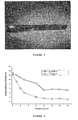
- the polystyrene film is welded to the stainless steel blade. It can be seen in particular that the blade can be lifted just by holding the assembly by the non-welded end of the polystyrene film, as illustrated by photographs A and B of FIG. figure 2 .
- Example 4 Thermofusion welding of two 316L stainless steel blades
- Two 316L stainless steel blades 10 cm long by 1 cm are pretreated identically. broadly by an electrografted poly-MMA film about 300 nm thick, according to a protocol similar to that described in Example 2.
- the two plates are superimposed and a polystyrene film 2 cm long and 1 cm wide and 75 ⁇ m thick is inserted between them at one of their ends.
- the sandwich thus obtained is clamped with a clamp, on an area measuring approximately 2 cm long and 1 cm wide.
- the whole is placed in an oven at 200 ° C for 2 days.
- Example 5 Bonding Bonding of a Polylactic Acid Film on a 316L Stainless Steel Blade
- This example illustrates the advantage provided by a bonding weld, produced by the process according to the invention, between a polylactic acid film (PLA) and a 316L stainless steel surface, on the stability of the interface resulting from this bonding. .
- PLA polylactic acid film
- the slides thus prepared are put in an oven at 40 ° C. for 4 hours. Each of them is then each introduced into a closed container containing an aqueous solution of PBS buffer pH 7.4, and placed in an incubator at 37 ° C with stirring.
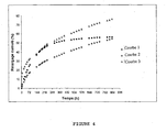
- Curves 2 and 3 show that after a "burst" of very rapid release due to a diffusion of pentoxifylline in excess, the pentoxifylline release profiles by PLA films welded to the stainless steel blades previously treated with an electro-grafted poly-BuMa film, become linear and ensure a gradual delivery of this compound. An inspection of these blades shows, moreover, no local deterioration (peeling for example) of PLA films. This means that the PLA / poly-BuMA interface is sufficiently solid to resist the release medium and suggests that the release would only be due to a progressive hydrolysis of the PLA at its surface in contact with the aqueous solution.
- this example demonstrates that the method according to the invention makes it possible to fix firmly, on a metal surface, a film of a biocompatible polymer such as PLA, without having to modify this polymer beforehand - which eliminates any risk of altering the biocompatibility - and in addition to including a fragile molecule, very sensitive to heat and temperature like pentoxifylline, in this film.
- a biocompatible polymer such as PLA
- the method according to the invention can be very useful for coating medical or surgical equipment, and in particular implants, with biocompatible materials, and in particular with materials for controlled release of biologically active substances.
- Example 6 Bonding Bonding of a Polyorthoester Film (POE) on a 316L Stainless Steel Blade
- This example also illustrates the advantage provided by a bonding weld, produced by the process according to the invention, between a polyorthoester film (POE) and a 316L stainless steel surface, on the stability of the interface resulting from this bonding.
- a bonding weld produced by the process according to the invention, between a polyorthoester film (POE) and a 316L stainless steel surface, on the stability of the interface resulting from this bonding.
- electrografting of a poly-BuMA film approximately 300 nm thick is carried out on a stainless steel blade 316L 10 cm long and 1 cm wide according to the same protocol as that described in Example 2.
- a solution of POE at 5% (m / m) in tetrahydrofuran (THF) is prepared, the latter being indeed a solvent for POE and a swelling of poly-BuMA.
- THF tetrahydrofuran
- a film with a thickness of about 500 nm POE is deposited on the stainless steel strip covered with the electro-grafted poly-BuMA film and on a non-pretreated stainless steel strip. an electro-grafted poly-BuMA film.
- the slides are dried in an oven at 40 ° C for 6 hours. They are then incubated according to the same protocol as that described in Example 5.
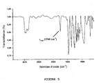
- the slides are taken out, drained and dried under a current of argon, and one appreciates the erosion of the POE films covering these blades while following the evolution of the transmittance of the band of carbonyl groups of POE with 1745 cm - 1 as measured by IRRAS spectroscopy, as a function of time.
- the figure 5 which corresponds to the IRRAS spectrum of a 500 nm thick POE film (ie the initial thickness of the POE films used in the present example) deposited on a stainless steel strip, shows the band of the carbonyl groups of the POE located at the wave number 1745 cm -1 and used to monitor the erosion of POE films.
- the figure 6 whose y-axis represents the transmittance (in percentages) of the band of carbonyl groups, while the x-axis represents the time (in days), represents the erosion profile of the POE film welded onto the stainless steel blade pretreated with an electro-grafted poly-BuMa film (curve 2) and that of the POE film deposited on the unpretreated stainless steel strip (curve 1) ).
Landscapes
- Chemical & Material Sciences (AREA)
- Organic Chemistry (AREA)
- Engineering & Computer Science (AREA)
- Materials Engineering (AREA)
- Health & Medical Sciences (AREA)
- Chemical Kinetics & Catalysis (AREA)
- Medicinal Chemistry (AREA)
- Manufacturing & Machinery (AREA)
- Polymers & Plastics (AREA)
- Life Sciences & Earth Sciences (AREA)
- Molecular Biology (AREA)
- Wood Science & Technology (AREA)
- Manufacture Of Macromolecular Shaped Articles (AREA)
- Lining Or Joining Of Plastics Or The Like (AREA)
- Adhesives Or Adhesive Processes (AREA)
- Polyoxymethylene Polymers And Polymers With Carbon-To-Carbon Bonds (AREA)
- Materials For Medical Uses (AREA)
Claims (16)
- Verfahren zum Verschweißen von zwei Objekten miteinander, von denen eines eine Polymeroberfläche umfasst und das andere eine elektrisch leitende oder halbleitende Oberfläche umfaßt, dadurch gekennzeichnet, dass es umfaßt:a) Elektropfropfen eines organischen Films auf die leitende oder halbleitende Oberfläche, und anschließendb) einen Arbeitsschritt des Verschweißens der Polymeroberfläche mit der derart gepfropften leitenden oder halbleitenden Oberfläche.
- Verfahren nach Anspruch 1, dadurch gekennzeichnet, dass das Elektropfropfen des organischen Films ein elektroinitiiertes Pfropfen ist.
- Verfahren nach Anspruch 2, dadurch gekennzeichnet, dass der organische Film ein Polymerfilm ist.
- Verfahren nach Anspruch 3, dadurch gekennzeichnet, dass der Polymerfilm ausgehend von Monomeren und/oder Präpolymeren erhalten wird, die partiell oder vollständig durch Vinylgruppen funktionalisiert sind.
- Verfahren nach Anspruch 4, dadurch gekennzeichnet, dass der Polymerfilm ausgehend von einem Vinylmonomer erhalten wird, welches ausgewählt ist aus Acrylonitril, Methacrylonitril, den Acrylaten und Methacrylaten, den Acrylamiden und Methacrylamiden, den Cyanoacrylaten, Acrylsäure und Methacrylsäure, Styrol, den Vinylhalogeniden, N-Vinyl Pyrrolidon, 2-Vinylpyridin, 4-Vinylpyridin und den telechelischen Verbindungen mit Vinylenden.
- Verfahren nach Anspruch 3, dadurch gekennzeichnet, dass der Polymerfilm ausgehend von Monomeren und/oder Präpolymeren erhalten wird, die partiell oder vollständig durch zyklische Gruppen funktionalisiert sind, welche durch einen nukleophilen oder elektrophilen Angriff spaltbar sind.
- Verfahren nach Anspruch 2, dadurch gekennzeichnet, dass der organische Film erhalten wird ausgehend von Diazonium-, Sulfonium-, Phosphonium-, lodoniumsalzen und ihren Mischungen.
- Verfahren nach einem der vorhergehenden Ansprüche, dadurch gekennzeichnet, dass der Arbeifisschritt des Verschweißens aus einer Thermofusion oder einer Verklebung oder einer Kombination der beiden besteht.
- Verfahren nach Anspruch 8, dadurch gekennzeichnet, dass die Verklebung mit Hilfe einer Substanz durchgeführt wird, die dazu ausgelegt ist, die zu verschweißende Polymeroberfläche sowie den auf die leitende oder halbleitende Oberfläche elektrogepfropften organischen Film aufzulösen oder aufzublähen.
- Verfahren nach einem der vorhergehenden Ansprüche, dadurch gekennzeichnet, dass das Polymer, welches die Polymeroberfläche bildet, ausgewählt ist aus den Polyethylenen, den Polypropylenen, den Polystyrolen, den Polyacrylonitrilen, den Polysiloxanen, den Polyestern, den Polyorthoestern, den Polycaprolaktonen, den Polybutyrolaktonen, den Polyacrylen, den Polymethacrylen, den Polyacrylamiden, den Epoxidharzen, ihren Copolymeren und ihren Mischungen.
- Verfahren nach einem der vorhergehenden Ansprüche, dadurch gekennzeichnet, dass das Polymer, welches die Polymeroberfläche bildet, ein thermofusionsfähiges Polymer ist.
- Verfahren nach einem der vorhergehenden Anspruche, dadurch gekennzeichnet, dass die Polymeroberfläche ein Polymerfilm ist, welcher ein leitendes oder halbleitendes Material bedeckt.
- Anwendung des Verfahrens nach einem der Ansprüche 1 bis 12 auf die Herstellung oder die Erneuerung von Verbundmaterialien, die für die Luftfahrt-, die Raumfahrt-, die Automobil-, die Biomedizin-, die Mikroelektronik- und die Mikrosystem-Industrien bestimmt sind.
- Anwendung des Verfahrens nach einem der Ansprüche 1 bis 12 auf die Herstellung von implantierbarem medizinischen und chirurgischen Material.
- Anwendung des Verfahrens nach einem der Ansprüche 1 bis 12 auf den Zusammenbau empfindlicher Elemente als Bestandteil von Mikrosystemen oder auf die Einkapselung von Mikrosystemen.
- Struktur mit zwei Objekten, von denen eines eine elektrisch leistende oder halbleitende Oberfläche umfasst und das andere eine Polymeroberfläche umfasst, wobei diese Oberflächen miteinander verschweißt sind mit Hilfe eines organischen Films mit einer Dicke von weniger als 1 µm, der auf die elektrisch leitende oder halbleitende Oberfläche elektrogepfropft ist.
Applications Claiming Priority (3)
| Application Number | Priority Date | Filing Date | Title |
|---|---|---|---|
| FR0210565A FR2843756B1 (fr) | 2002-08-26 | 2002-08-26 | Procede de soudage d'une surface polymere avec une surface conductrice ou semi-conductrice et ses applications |
| FR0210565 | 2002-08-26 | ||
| PCT/FR2003/050037 WO2004018548A2 (fr) | 2002-08-26 | 2003-08-25 | Procede de soudage d'une surface polymere avec une surface conductrice ou semi-conductrice |
Publications (2)
| Publication Number | Publication Date |
|---|---|
| EP1532197A2 EP1532197A2 (de) | 2005-05-25 |
| EP1532197B1 true EP1532197B1 (de) | 2012-06-13 |
Family
ID=31198301
Family Applications (1)
| Application Number | Title | Priority Date | Filing Date |
|---|---|---|---|
| EP03773828A Expired - Lifetime EP1532197B1 (de) | 2002-08-26 | 2003-08-25 | Verfahren zum schweissen einer polymeren oberfläche mit einer elektrisch leitenden oder halbleitendem oberfläche |
Country Status (9)
| Country | Link |
|---|---|
| US (1) | US7605050B2 (de) |
| EP (1) | EP1532197B1 (de) |
| JP (1) | JP4339253B2 (de) |
| AU (2) | AU2003282208A1 (de) |
| BR (1) | BRPI0314404B1 (de) |
| CA (1) | CA2496118C (de) |
| ES (1) | ES2389468T3 (de) |
| FR (1) | FR2843756B1 (de) |
| WO (1) | WO2004018548A2 (de) |
Families Citing this family (31)
| Publication number | Priority date | Publication date | Assignee | Title |
|---|---|---|---|---|
| US20100038119A1 (en) * | 1999-08-27 | 2010-02-18 | Lex Kosowsky | Metal Deposition |
| US20100038121A1 (en) * | 1999-08-27 | 2010-02-18 | Lex Kosowsky | Metal Deposition |
| WO2001017320A1 (en) | 1999-08-27 | 2001-03-08 | Lex Kosowsky | Current carrying structure using voltage switchable dielectric material |
| US20100040896A1 (en) * | 1999-08-27 | 2010-02-18 | Lex Kosowsky | Metal Deposition |
| EP1969627A4 (de) | 2005-11-22 | 2010-01-20 | Shocking Technologies Inc | Halbleiteranordnungen mit spannungsumschaltbaren materialien für überspannungsschutz |
| JP5236503B2 (ja) * | 2006-02-28 | 2013-07-17 | コミサリア ア レネルジィ アトミーク エ オ ゼネ ルジイ アルテアナティーフ | 水溶液から導電性または半導電性表面上に有機フィルムを形成する方法 |
| JP5650377B2 (ja) | 2006-02-28 | 2015-01-07 | アルシメールAlchimer | 導電性または半導電性表面上に有機電気グラフト化被膜を形成する方法 |
| FR2902102B1 (fr) | 2006-06-07 | 2011-11-18 | Univ Paris 13 | Procede de greffage de polymeres bioactifs sur des materiaux prothetiques |
| CA2653156C (en) * | 2006-06-13 | 2012-12-18 | Christophe Bureau | Drug eluting stent with a biodegradable release layer attached with an electro-grafted primer coating |
| US11039942B2 (en) * | 2006-06-13 | 2021-06-22 | Sino Medical Sciences Technology Inc. | Drug eluting stent and method of use of the same for enabling restoration of functional endothelial cell layers |
| KR20090055017A (ko) | 2006-09-24 | 2009-06-01 | 쇼킹 테크놀로지스 인코포레이티드 | 스탭 전압 응답을 가진 전압 가변 유전 재료를 위한 조성물및 그 제조 방법 |
| WO2008090555A2 (en) * | 2007-01-22 | 2008-07-31 | Elutex Ltd. | Medical devices having a matrix adhered thereof |
| FR2929137B1 (fr) * | 2008-03-28 | 2011-03-11 | Commissariat Energie Atomique | Procede d'electrogreffage localise sur des substrats conducteurs ou semi-conducteurs en presence d'une microelectrode |
| US9226391B2 (en) | 2009-01-27 | 2015-12-29 | Littelfuse, Inc. | Substrates having voltage switchable dielectric materials |
| US8399773B2 (en) | 2009-01-27 | 2013-03-19 | Shocking Technologies, Inc. | Substrates having voltage switchable dielectric materials |
| US8272123B2 (en) | 2009-01-27 | 2012-09-25 | Shocking Technologies, Inc. | Substrates having voltage switchable dielectric materials |
| WO2010110909A1 (en) | 2009-03-26 | 2010-09-30 | Shocking Technologies, Inc. | Components having voltage switchable dielectric materials |
| FR2954330B1 (fr) * | 2009-12-23 | 2013-01-04 | Valois Sas | Procede de traitement de surface d'un dispositif de distribution de produit fluide. |
| FR2954326B1 (fr) * | 2009-12-23 | 2013-01-18 | Valois Sas | Procede de traitement de surface d'un dispositif de distribution de produit fluide. |
| WO2011082379A1 (en) * | 2010-01-03 | 2011-07-07 | Alchimer, S.A. | Solar cells |
| US20110162701A1 (en) * | 2010-01-03 | 2011-07-07 | Claudio Truzzi | Photovoltaic Cells |
| US9224728B2 (en) | 2010-02-26 | 2015-12-29 | Littelfuse, Inc. | Embedded protection against spurious electrical events |
| US9320135B2 (en) | 2010-02-26 | 2016-04-19 | Littelfuse, Inc. | Electric discharge protection for surface mounted and embedded components |
| US9082622B2 (en) | 2010-02-26 | 2015-07-14 | Littelfuse, Inc. | Circuit elements comprising ferroic materials |
| US8647535B2 (en) | 2011-01-07 | 2014-02-11 | International Business Machines Corporation | Conductive metal and diffusion barrier seed compositions, and methods of use in semiconductor and interlevel dielectric substrates |
| CN103536971A (zh) * | 2012-07-12 | 2014-01-29 | 赛诺医疗科学技术有限公司 | 药物可控释放的药物洗脱医疗器械及其制备方法 |
| FR3014116A1 (fr) * | 2013-12-04 | 2015-06-05 | Commissariat Energie Atomique | Primaire d'adherence pour peinture |
| US11097986B2 (en) | 2015-05-29 | 2021-08-24 | Raytheon Technologies Corporation | Preceramic ionic systems |
| WO2019202067A1 (en) * | 2018-04-20 | 2019-10-24 | Aveni | Method for temporary or permanent wafer bonding |
| US11121302B2 (en) | 2018-10-11 | 2021-09-14 | SeeQC, Inc. | System and method for superconducting multi-chip module |
| CN111893534A (zh) * | 2020-06-13 | 2020-11-06 | 郑州大学 | 一种生物镁合金表面聚己内酯涂层的制备方法 |
Family Cites Families (19)
| Publication number | Priority date | Publication date | Assignee | Title |
|---|---|---|---|---|
| DE152573C (de) | 1903-04-18 | |||
| DD152573A1 (de) * | 1980-07-14 | 1981-12-02 | Wolfgang Kleber | Herstellungsverfahren fuer durch klebverbindungen zusammengesetzte erzeugnisse |
| US4421569A (en) | 1982-05-07 | 1983-12-20 | Sharon Tube Corp. | Corrosion protection of steel pipes |
| DE3327012A1 (de) * | 1983-07-27 | 1985-02-07 | Basf Ag, 6700 Ludwigshafen | Verfahren zur elektrochemischen polymerisation von pyrrolen, anode zur durchfuehrung dieses verfahrens sowie nach diesem verfahren erhaltene produkte |
| JP2929651B2 (ja) * | 1990-03-14 | 1999-08-03 | 株式会社ブリヂストン | ゴム系複合材料の製造方法 |
| US5599352A (en) | 1992-03-19 | 1997-02-04 | Medtronic, Inc. | Method of making a drug eluting stent |
| KR100242404B1 (ko) * | 1995-08-28 | 2000-03-02 | 에모토 간지 | 유기 피복 도금 강판 및 그의 제조방법 |
| US6136274A (en) | 1996-10-07 | 2000-10-24 | Irori | Matrices with memories in automated drug discovery and units therefor |
| WO1998022542A2 (en) | 1996-11-08 | 1998-05-28 | Ikonos Corporation | Chemical functionalization of surfaces |
| US5997517A (en) | 1997-01-27 | 1999-12-07 | Sts Biopolymers, Inc. | Bonding layers for medical device surface coatings |
| GB2324530A (en) | 1997-04-25 | 1998-10-28 | Polybiomed Ltd | Introduction of functional groups on polymers |
| US6335571B1 (en) * | 1997-07-21 | 2002-01-01 | Miguel Albert Capote | Semiconductor flip-chip package and method for the fabrication thereof |
| US5858653A (en) | 1997-09-30 | 1999-01-12 | Surmodics, Inc. | Reagent and method for attaching target molecules to a surface |
| US6287687B1 (en) | 1998-05-08 | 2001-09-11 | Asten, Inc. | Structures and components thereof having a desired surface characteristic together with methods and apparatuses for producing the same |
| FR2780200B1 (fr) * | 1998-06-22 | 2003-09-05 | Commissariat Energie Atomique | Dispositif et procede de formation d'un dispositif presentant une cavite a atmosphere controlee |
| FR2781232B1 (fr) | 1998-07-15 | 2000-09-08 | Centre Nat Rech Scient | Polymere reactif utilisable pour la separation et l'adsorption de substances organiques, et materiau le contenant |
| US6444326B1 (en) | 1999-03-05 | 2002-09-03 | Restek Corporation | Surface modification of solid supports through the thermal decomposition and functionalization of silanes |
| DE19962272A1 (de) | 1999-12-23 | 2001-06-28 | Basf Ag | Isocyanatgruppen aufweisende Bausteine sowie ihre Verwendung zur Funktionalisierung oder Modifizierung von Verbindungen oder Oberflächen |
| EP1425315A2 (de) | 2001-06-04 | 2004-06-09 | University of Liege | Verfahren zur abscheidung einer stark adhärenten polymerbeschichtung auf eine elektrisch leitfähige oberfläche |
-
2002
- 2002-08-26 FR FR0210565A patent/FR2843756B1/fr not_active Expired - Fee Related
-
2003
- 2003-08-25 ES ES03773828T patent/ES2389468T3/es not_active Expired - Lifetime
- 2003-08-25 CA CA2496118A patent/CA2496118C/fr not_active Expired - Lifetime
- 2003-08-25 US US10/525,592 patent/US7605050B2/en not_active Expired - Lifetime
- 2003-08-25 BR BRPI0314404A patent/BRPI0314404B1/pt not_active IP Right Cessation
- 2003-08-25 WO PCT/FR2003/050037 patent/WO2004018548A2/fr not_active Ceased
- 2003-08-25 EP EP03773828A patent/EP1532197B1/de not_active Expired - Lifetime
- 2003-08-25 AU AU2003282208A patent/AU2003282208A1/en not_active Abandoned
- 2003-08-25 JP JP2004530315A patent/JP4339253B2/ja not_active Expired - Lifetime
-
2009
- 2009-09-07 AU AU2009213012A patent/AU2009213012B2/en not_active Expired
Also Published As
| Publication number | Publication date |
|---|---|
| FR2843756B1 (fr) | 2005-04-22 |
| JP4339253B2 (ja) | 2009-10-07 |
| EP1532197A2 (de) | 2005-05-25 |
| US20050255631A1 (en) | 2005-11-17 |
| CA2496118A1 (fr) | 2004-03-04 |
| WO2004018548A3 (fr) | 2004-04-08 |
| BR0314404A (pt) | 2005-07-19 |
| ES2389468T3 (es) | 2012-10-26 |
| AU2009213012B2 (en) | 2011-04-28 |
| AU2009213012A1 (en) | 2009-10-08 |
| AU2003282208A1 (en) | 2004-03-11 |
| WO2004018548A2 (fr) | 2004-03-04 |
| BRPI0314404B1 (pt) | 2016-09-27 |
| CA2496118C (fr) | 2012-09-25 |
| US7605050B2 (en) | 2009-10-20 |
| FR2843756A1 (fr) | 2004-02-27 |
| JP2005536601A (ja) | 2005-12-02 |
Similar Documents
| Publication | Publication Date | Title |
|---|---|---|
| EP1532197B1 (de) | Verfahren zum schweissen einer polymeren oberfläche mit einer elektrisch leitenden oder halbleitendem oberfläche | |
| EP1595001B1 (de) | Oberflächenbeschichtungsverfahren | |
| DK2920230T3 (en) | JOINT POLYMER AND SURFACE MODIFIED SOLID PART | |
| CN108884182B (zh) | 导电聚合物 | |
| FR2929618A1 (fr) | Procede pour assembler deux surfaces ou une surface avec une molecule d'interet | |
| FR2843757A1 (fr) | Procede de garniture d'une surface par un film organique | |
| JP4403459B2 (ja) | 官能化された電気導体または半導体表面を含む固体支持体、その調製方法及びその使用 | |
| EP4045550B1 (de) | Polymergele zur herstellung von polymerbürsten | |
| EP1490444B1 (de) | Verfahren zur fixierung von makroobjekten auf einer elektrischleitenden oder halbleitenden fläche durch elektropfropfen, so erhaltene flächen und deren verwendung | |
| FR2910006A1 (fr) | Procede de preparation d'un film organique a la surface d'un support solide dans des conditions non-electrochimiques, support solide ainsi obtenu et kit de preparation | |
| FR2910007A1 (fr) | Procede de preparation d'un film organique a la surface d'un support solide dans des conditions non-electrochimiques, support solide ainsi obtenu et kit de preparation | |
| FR2921516A1 (fr) | Procede d'electrogreffage localise sur des substrats semi-conducteurs photosensibles | |
| EP2720806B1 (de) | Verfahren zur funktionalisierung einer oberfläche mit einem bestimmten objekt oder molekül | |
| JP2014502672A (ja) | 基体の表面にポリマー層を電気触媒反応で化学的にグラフトさせることによるコーティング方法 | |
| EP1476756B1 (de) | Komponente für ein mikrosystem zur biologischen oder biochemischen analyse | |
| Jodeiri | Development of 3D printed enzymatic biofuel cells for powering implantable biomedical devices | |
| EP1476755A1 (de) | Werbundmaterial für mykrosystem für biologische oder biochemische analyse | |
| Kim et al. | Electrochemically active, anti-biofouling polymer adlayers on indium-tin-oxide electrodes | |
| FR2977812A1 (fr) | Procede de preparation d'un film organique hydrophobe a la surface d'un support solide |
Legal Events
| Date | Code | Title | Description |
|---|---|---|---|
| PUAI | Public reference made under article 153(3) epc to a published international application that has entered the european phase |
Free format text: ORIGINAL CODE: 0009012 |
|
| 17P | Request for examination filed |
Effective date: 20050128 |
|
| AK | Designated contracting states |
Kind code of ref document: A2 Designated state(s): AT BE BG CH CY CZ DE DK EE ES FI FR GB GR HU IE IT LI LU MC NL PT RO SE SI SK TR |
|
| AX | Request for extension of the european patent |
Extension state: AL LT LV MK |
|
| DAX | Request for extension of the european patent (deleted) | ||
| RAP1 | Party data changed (applicant data changed or rights of an application transferred) |
Owner name: ALCHIMER S.A. Owner name: COMMISSARIAT A L'ENERGIE ATOMIQUE |
|
| RAP1 | Party data changed (applicant data changed or rights of an application transferred) |
Owner name: ALCHIMER S.A. Owner name: COMMISSARIAT A L'ENERGIE ATOMIQUE ET AUX ENERGIES |
|
| RAP1 | Party data changed (applicant data changed or rights of an application transferred) |
Owner name: ALCHIMEDICS Owner name: COMMISSARIAT A L'ENERGIE ATOMIQUE ET AUX ENERGIES |
|
| 17Q | First examination report despatched |
Effective date: 20110302 |
|
| RTI1 | Title (correction) |
Free format text: METHOD OF SOLDERING A POLYMER SURFACE WITH AN ELECTRICALLY CONDUCTIVE OR SEMICONDUCTIVE SURFACE AND APPLICATIONS OF SAME |
|
| GRAP | Despatch of communication of intention to grant a patent |
Free format text: ORIGINAL CODE: EPIDOSNIGR1 |
|
| GRAS | Grant fee paid |
Free format text: ORIGINAL CODE: EPIDOSNIGR3 |
|
| GRAA | (expected) grant |
Free format text: ORIGINAL CODE: 0009210 |
|
| AK | Designated contracting states |
Kind code of ref document: B1 Designated state(s): AT BE BG CH CY CZ DE DK EE ES FI FR GB GR HU IE IT LI LU MC NL PT RO SE SI SK TR |
|
| REG | Reference to a national code |
Ref country code: GB Ref legal event code: FG4D Free format text: NOT ENGLISH |
|
| REG | Reference to a national code |
Ref country code: AT Ref legal event code: REF Ref document number: 561980 Country of ref document: AT Kind code of ref document: T Effective date: 20120615 Ref country code: CH Ref legal event code: EP |
|
| REG | Reference to a national code |
Ref country code: IE Ref legal event code: FG4D Free format text: LANGUAGE OF EP DOCUMENT: FRENCH |
|
| REG | Reference to a national code |
Ref country code: DE Ref legal event code: R096 Ref document number: 60341293 Country of ref document: DE Effective date: 20120809 |
|
| REG | Reference to a national code |
Ref country code: NL Ref legal event code: VDEP Effective date: 20120613 |
|
| REG | Reference to a national code |
Ref country code: ES Ref legal event code: FG2A Ref document number: 2389468 Country of ref document: ES Kind code of ref document: T3 Effective date: 20121026 |
|
| PG25 | Lapsed in a contracting state [announced via postgrant information from national office to epo] |
Ref country code: FI Free format text: LAPSE BECAUSE OF FAILURE TO SUBMIT A TRANSLATION OF THE DESCRIPTION OR TO PAY THE FEE WITHIN THE PRESCRIBED TIME-LIMIT Effective date: 20120613 Ref country code: CY Free format text: LAPSE BECAUSE OF FAILURE TO SUBMIT A TRANSLATION OF THE DESCRIPTION OR TO PAY THE FEE WITHIN THE PRESCRIBED TIME-LIMIT Effective date: 20120613 Ref country code: SE Free format text: LAPSE BECAUSE OF FAILURE TO SUBMIT A TRANSLATION OF THE DESCRIPTION OR TO PAY THE FEE WITHIN THE PRESCRIBED TIME-LIMIT Effective date: 20120613 |
|
| REG | Reference to a national code |
Ref country code: AT Ref legal event code: MK05 Ref document number: 561980 Country of ref document: AT Kind code of ref document: T Effective date: 20120613 |
|
| PG25 | Lapsed in a contracting state [announced via postgrant information from national office to epo] |
Ref country code: SI Free format text: LAPSE BECAUSE OF FAILURE TO SUBMIT A TRANSLATION OF THE DESCRIPTION OR TO PAY THE FEE WITHIN THE PRESCRIBED TIME-LIMIT Effective date: 20120613 Ref country code: GR Free format text: LAPSE BECAUSE OF FAILURE TO SUBMIT A TRANSLATION OF THE DESCRIPTION OR TO PAY THE FEE WITHIN THE PRESCRIBED TIME-LIMIT Effective date: 20120914 |
|
| PG25 | Lapsed in a contracting state [announced via postgrant information from national office to epo] |
Ref country code: EE Free format text: LAPSE BECAUSE OF FAILURE TO SUBMIT A TRANSLATION OF THE DESCRIPTION OR TO PAY THE FEE WITHIN THE PRESCRIBED TIME-LIMIT Effective date: 20120613 Ref country code: RO Free format text: LAPSE BECAUSE OF FAILURE TO SUBMIT A TRANSLATION OF THE DESCRIPTION OR TO PAY THE FEE WITHIN THE PRESCRIBED TIME-LIMIT Effective date: 20120613 Ref country code: CZ Free format text: LAPSE BECAUSE OF FAILURE TO SUBMIT A TRANSLATION OF THE DESCRIPTION OR TO PAY THE FEE WITHIN THE PRESCRIBED TIME-LIMIT Effective date: 20120613 Ref country code: SK Free format text: LAPSE BECAUSE OF FAILURE TO SUBMIT A TRANSLATION OF THE DESCRIPTION OR TO PAY THE FEE WITHIN THE PRESCRIBED TIME-LIMIT Effective date: 20120613 Ref country code: AT Free format text: LAPSE BECAUSE OF FAILURE TO SUBMIT A TRANSLATION OF THE DESCRIPTION OR TO PAY THE FEE WITHIN THE PRESCRIBED TIME-LIMIT Effective date: 20120613 |
|
| BERE | Be: lapsed |
Owner name: ALCHIMEDICS Effective date: 20120831 Owner name: COMMISSARIAT A L'ENERGIE ATOMIQUE ET AUX ENERGIES Effective date: 20120831 |
|
| PG25 | Lapsed in a contracting state [announced via postgrant information from national office to epo] |
Ref country code: PT Free format text: LAPSE BECAUSE OF FAILURE TO SUBMIT A TRANSLATION OF THE DESCRIPTION OR TO PAY THE FEE WITHIN THE PRESCRIBED TIME-LIMIT Effective date: 20121015 |
|
| REG | Reference to a national code |
Ref country code: CH Ref legal event code: PL |
|
| PG25 | Lapsed in a contracting state [announced via postgrant information from national office to epo] |
Ref country code: MC Free format text: LAPSE BECAUSE OF NON-PAYMENT OF DUE FEES Effective date: 20120831 Ref country code: NL Free format text: LAPSE BECAUSE OF FAILURE TO SUBMIT A TRANSLATION OF THE DESCRIPTION OR TO PAY THE FEE WITHIN THE PRESCRIBED TIME-LIMIT Effective date: 20120613 |
|
| PLBE | No opposition filed within time limit |
Free format text: ORIGINAL CODE: 0009261 |
|
| STAA | Information on the status of an ep patent application or granted ep patent |
Free format text: STATUS: NO OPPOSITION FILED WITHIN TIME LIMIT |
|
| PG25 | Lapsed in a contracting state [announced via postgrant information from national office to epo] |
Ref country code: CH Free format text: LAPSE BECAUSE OF NON-PAYMENT OF DUE FEES Effective date: 20120831 Ref country code: DK Free format text: LAPSE BECAUSE OF FAILURE TO SUBMIT A TRANSLATION OF THE DESCRIPTION OR TO PAY THE FEE WITHIN THE PRESCRIBED TIME-LIMIT Effective date: 20120613 Ref country code: LI Free format text: LAPSE BECAUSE OF NON-PAYMENT OF DUE FEES Effective date: 20120831 |
|
| 26N | No opposition filed |
Effective date: 20130314 |
|
| PG25 | Lapsed in a contracting state [announced via postgrant information from national office to epo] |
Ref country code: BE Free format text: LAPSE BECAUSE OF NON-PAYMENT OF DUE FEES Effective date: 20120831 |
|
| REG | Reference to a national code |
Ref country code: DE Ref legal event code: R097 Ref document number: 60341293 Country of ref document: DE Effective date: 20130314 |
|
| PG25 | Lapsed in a contracting state [announced via postgrant information from national office to epo] |
Ref country code: BG Free format text: LAPSE BECAUSE OF FAILURE TO SUBMIT A TRANSLATION OF THE DESCRIPTION OR TO PAY THE FEE WITHIN THE PRESCRIBED TIME-LIMIT Effective date: 20120913 |
|
| PG25 | Lapsed in a contracting state [announced via postgrant information from national office to epo] |
Ref country code: TR Free format text: LAPSE BECAUSE OF FAILURE TO SUBMIT A TRANSLATION OF THE DESCRIPTION OR TO PAY THE FEE WITHIN THE PRESCRIBED TIME-LIMIT Effective date: 20120613 |
|
| PG25 | Lapsed in a contracting state [announced via postgrant information from national office to epo] |
Ref country code: LU Free format text: LAPSE BECAUSE OF NON-PAYMENT OF DUE FEES Effective date: 20120825 |
|
| PG25 | Lapsed in a contracting state [announced via postgrant information from national office to epo] |
Ref country code: HU Free format text: LAPSE BECAUSE OF FAILURE TO SUBMIT A TRANSLATION OF THE DESCRIPTION OR TO PAY THE FEE WITHIN THE PRESCRIBED TIME-LIMIT Effective date: 20030825 |
|
| REG | Reference to a national code |
Ref country code: FR Ref legal event code: PLFP Year of fee payment: 14 |
|
| REG | Reference to a national code |
Ref country code: FR Ref legal event code: PLFP Year of fee payment: 15 |
|
| REG | Reference to a national code |
Ref country code: FR Ref legal event code: PLFP Year of fee payment: 16 |
|
| PGFP | Annual fee paid to national office [announced via postgrant information from national office to epo] |
Ref country code: IT Payment date: 20220831 Year of fee payment: 20 Ref country code: IE Payment date: 20220819 Year of fee payment: 20 Ref country code: GB Payment date: 20220824 Year of fee payment: 20 Ref country code: ES Payment date: 20220919 Year of fee payment: 20 Ref country code: DE Payment date: 20220822 Year of fee payment: 20 |
|
| PGFP | Annual fee paid to national office [announced via postgrant information from national office to epo] |
Ref country code: FR Payment date: 20220822 Year of fee payment: 20 |
|
| REG | Reference to a national code |
Ref country code: DE Ref legal event code: R071 Ref document number: 60341293 Country of ref document: DE |
|
| REG | Reference to a national code |
Ref country code: ES Ref legal event code: FD2A Effective date: 20230901 |
|
| REG | Reference to a national code |
Ref country code: GB Ref legal event code: PE20 Expiry date: 20230824 |
|
| REG | Reference to a national code |
Ref country code: IE Ref legal event code: MK9A |
|
| PG25 | Lapsed in a contracting state [announced via postgrant information from national office to epo] |
Ref country code: IE Free format text: LAPSE BECAUSE OF EXPIRATION OF PROTECTION Effective date: 20230825 Ref country code: GB Free format text: LAPSE BECAUSE OF EXPIRATION OF PROTECTION Effective date: 20230824 Ref country code: ES Free format text: LAPSE BECAUSE OF EXPIRATION OF PROTECTION Effective date: 20230826 |