EP1529301B1 - Elektrothermisch betätigter mikroelektromechanischer schalter mit bistabilem knickbalken - Google Patents
Elektrothermisch betätigter mikroelektromechanischer schalter mit bistabilem knickbalken Download PDFInfo
- Publication number
- EP1529301B1 EP1529301B1 EP03759192A EP03759192A EP1529301B1 EP 1529301 B1 EP1529301 B1 EP 1529301B1 EP 03759192 A EP03759192 A EP 03759192A EP 03759192 A EP03759192 A EP 03759192A EP 1529301 B1 EP1529301 B1 EP 1529301B1
- Authority
- EP
- European Patent Office
- Prior art keywords
- electro
- thermal actuator
- mems switch
- current passes
- mems
- Prior art date
- Legal status (The legal status is an assumption and is not a legal conclusion. Google has not performed a legal analysis and makes no representation as to the accuracy of the status listed.)
- Expired - Lifetime
Links
- 239000004020 conductor Substances 0.000 claims description 17
- 238000004891 communication Methods 0.000 claims description 10
- 230000005540 biological transmission Effects 0.000 claims description 6
- 238000000034 method Methods 0.000 claims description 5
- 230000007935 neutral effect Effects 0.000 description 11
- 238000010438 heat treatment Methods 0.000 description 6
- 239000000463 material Substances 0.000 description 5
- 238000003780 insertion Methods 0.000 description 4
- 230000037431 insertion Effects 0.000 description 4
- 230000008901 benefit Effects 0.000 description 3
- 238000004519 manufacturing process Methods 0.000 description 3
- 230000004913 activation Effects 0.000 description 2
- 238000010586 diagram Methods 0.000 description 2
- 238000005516 engineering process Methods 0.000 description 2
- 230000005669 field effect Effects 0.000 description 2
- 238000002955 isolation Methods 0.000 description 2
- 238000005459 micromachining Methods 0.000 description 2
- 239000000758 substrate Substances 0.000 description 2
- XUIMIQQOPSSXEZ-UHFFFAOYSA-N Silicon Chemical compound [Si] XUIMIQQOPSSXEZ-UHFFFAOYSA-N 0.000 description 1
- 230000009849 deactivation Effects 0.000 description 1
- 229910052710 silicon Inorganic materials 0.000 description 1
- 239000010703 silicon Substances 0.000 description 1
- 238000010897 surface acoustic wave method Methods 0.000 description 1
Images




Classifications
-
- H—ELECTRICITY
- H01—ELECTRIC ELEMENTS
- H01H—ELECTRIC SWITCHES; RELAYS; SELECTORS; EMERGENCY PROTECTIVE DEVICES
- H01H1/00—Contacts
- H01H1/0036—Switches making use of microelectromechanical systems [MEMS]
-
- H—ELECTRICITY
- H01—ELECTRIC ELEMENTS
- H01H—ELECTRIC SWITCHES; RELAYS; SELECTORS; EMERGENCY PROTECTIVE DEVICES
- H01H1/00—Contacts
- H01H1/0036—Switches making use of microelectromechanical systems [MEMS]
- H01H2001/0042—Bistable switches, i.e. having two stable positions requiring only actuating energy for switching between them, e.g. with snap membrane or by permanent magnet
-
- H—ELECTRICITY
- H01—ELECTRIC ELEMENTS
- H01H—ELECTRIC SWITCHES; RELAYS; SELECTORS; EMERGENCY PROTECTIVE DEVICES
- H01H37/00—Thermally-actuated switches
- H01H2037/008—Micromechanical switches operated thermally
-
- H—ELECTRICITY
- H01—ELECTRIC ELEMENTS
- H01H—ELECTRIC SWITCHES; RELAYS; SELECTORS; EMERGENCY PROTECTIVE DEVICES
- H01H37/00—Thermally-actuated switches
- H01H37/02—Details
- H01H37/32—Thermally-sensitive members
- H01H37/52—Thermally-sensitive members actuated due to deflection of bimetallic element
- H01H37/54—Thermally-sensitive members actuated due to deflection of bimetallic element wherein the bimetallic element is inherently snap acting
- H01H37/5409—Bistable switches; Resetting means
Definitions
- MEMS microelectromechanical systems
- MEMS switches i.e., contacts, relays, shunts, etc.
- FET field-effect transistor
- MEMS switches are generally much slower than solid-state switches. This limitation precludes applying MEMS switches in certain technologies where sub-microsecond switching is required, such as switching an antenna between transmit and receive in highspeed wireless communication devices.
- Smart antenna switching applications typically require switching speeds ranging from milliseconds to seconds depending on the systems.
- FIGS. 1 and 1A illustrate a prior art MEMS switch 10 that includes a beam 12 which is electro-thermally buckled.
- Beam 12 is formed of a high thermal expansion conductor 14 and a low thermal expansion dielectric 16.
- Conductor 14 and dielectric 16 are restrained at opposing ends by anchors 18A, 18B.
- FIG. 2 illustrates another prior art MEMS switch 30 that includes a beam 32 which is secured at opposite ends to anchors 34A, 34B.
- Beam 32 is secured to anchors 34A, 34B in a manner that places beam 32 under compressive stress. The compressive stress causes beam 32 to buckle. Beam 32 needs to remain in a buckled state for MEMS switch 30 to operate appropriately.
- a lateral actuation electrode 36 is positioned adjacent to beam 32 at the level beam 32 would occupy were it not buckled from the compressive stress. This level of beam 32 is referred to as the neutral position and is indicated in FIG. 2 with line 38.
- a voltage is applied to lateral actuation electrode 36 to generate an electrostatic force that pulls beam 32 up or down toward its neutral position.
- the inertia of beam 32 carries it past the neutral position to the other side where beam 32 electrically connects contacts (not shown) to allow signals to pass between the contacts.
- MEMS switch 30 does not require any power to maintain beam 32 in either the up or down position.
- One drawback associated with MEMS switch 30 is that large actuation voltages are required with electrostatic actuation in general, and in particular when electrostatic actuation is used to maneuver a buckled beam.
- WO 99/16096 A discloses a MEMS, according to the preamble of claim 1.
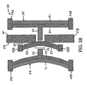
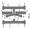
- a microelectromechanical systems (MEMS) switch 50 that includes a beam 52, a first electro-thermal actuator 54 and a second electro-thermal actuator 56 is shown in FIGS. 3A , 3B , 3C and 3D .
- the beam 52 has a first side 58 and a second side 60.
- First electro-thermal actuator 54 includes a first stud 62 that applies a force to the first side 58 of beam 52 as current passes through first electro-thermal actuator 54.
- second electro-thermal actuator 56 includes a second stud 64 that applies a force to the second side 60 of beam 52 as current passes through second electro-thermal actuator 56.
- Actuators 54, 56 may be connected to a circuit by bond pads or other conventional means so that the circuit can direct the supply of current to actuators 54, 56.
- beam 52 is fixed at opposing ends to anchors 68A, 68B. Beam 52 is under a compressive stress such that beam 52 is buckled.
- First electro-thermal actuator 54 is fixed at opposing ends to anchors 69A, 69B, and in some embodiments is made up of a high thermal expansion conductor 70 and a low thermal expansion dielectric 71.
- the resistive heating causes the first electro-thermal actuator 54 to buckle outward on the side of conductor 70 due to the difference in thermal expansion between conductor 70 and dielectric 71.
- Second electro-thermal actuator 56 is fixed at opposing ends to anchors 79A, 79B and may be similarly formed of a high thermal expansion conductor 80 and a low thermal expansion dielectric 81.
- the resistive heating causes second electro-thermal actuator 56 to buckle outward on the side of conductor 80 due to the difference in thermal expansion between conductor 80 and dielectric 81.
- second electro-thermal actuator 56 will continuously engage beam 52, while in other embodiments actuator 56 will engage beam 52 only until beam 52 moves past its neutral position. Once beam 52 moves past the neutral position, the compressive stress will cause beam 52 to buckle outward away from contacts 67A, 67B. Contact between actuators 54, 56 and beam 52 when beam 52 is engaged with contacts 67A, 67 B can cause interference with signals that are transferred between contacts 67A, 67B through beam 52.
- beam 100 is shown in FIG. 5 where beam 100 is unreleased and includes a dielectric body 102 covered with an electrical conductor 104. Electrical conductor 104 facilitates transferring signals between isolated contacts that become electrically connected by beam 100 during operation of a MEMS switch that includes beam 100.
- FIGS. 6A, 6B and 6C Another example beam 110 that may be used in MEMS switch 50 is shown in FIGS. 6A, 6B and 6C .
- Beam 110 is shown in an unreleased state in FIG. 6A and in a released state in FIG. 6B .
- Beam 110 has the same arc-shape before and after release such that it is not under compressive stress.
- one of the first and second electro-thermal actuators 54, 56 buckles beam 110 such that it is deflected into an opposing arc (see FIG. 6C ). Beam 110 is then forced by the other of the first and second actuators 54, 56 back into its original arc-shaped, unstressed state.
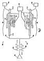
- FIG. 8 shows a schematic circuit diagram of a MEMS-based wireless communication system 800 that includes MEMS switches 830, 840.
- MEMS switches 830 and 840 are the same as MEMS switch 50 described above.
- MEMS switches 830, 840 have intrinsic advantages over their conventional solid-state counterparts (e.g., field-effect transistor (FET) switches), including superior power efficiency, low insertion loss and excellent isolation.
- FET field-effect transistor
- MEMS switches 830, 840 are suitable for switching an antenna 810 between transmit and receive in some wireless communication devices where sub-microsecond switching is not required.
- System 800 includes an antenna 810 for receiving a signal 814 and transmitting a signal 820.
- MEMS switches 830, 840 are electrically connected to antenna 810 via a branch circuit 844 having a first branch wire 846 and a second branch wire 848.
- a voltage source controller 912 selectively activates MEMS switches 830 and 840 so that received signal 814 can be transmitted from antenna 810 to receiver electronics 930 for processing, while transmitted signal 820 generated by transmitter electronics 940 can be passed to antenna 810 for transmission.
- MEMS switches 830, 840 are off when beams 52 are disengaged from respective contacts 67A, 67B.
- MEMS switches 830, 840 are individually turned on by selectively applying an actuation voltage to a respective first electro-thermal actuator 54 that is in each MEMS switch 830, 840. Applying an actuation voltage to the first electro-thermal actuators 54 causes each first electro-thermal actuator 54 to buckle.
- each respective MEMS switch 830, 840 buckles, it applies a force to beam 52 that is sufficient to buckle beam 52.
- beam 52 buckles it electrically connects contacts 67A, 67B such that a desired one of the corresponding signals 814, 820 passes between contacts 67A, 67B along the corresponding first or second branch wire 846, 848.
- MEMS switches 830, 840 are each turned off by selectively applying an actuation voltage to the respective second electro-thermal actuators 56 such that the second electro-thermal actuators 56 buckle and apply a force to respective beams 52 that is sufficient to buckle beams 52 away from contacts 67A, 67B.
- voltage source controller 912 includes logic for selectively supplying voltages to actuators 54, 56 in each MEMS switch 830, 840 permitting selective activation and deactivation of MEMS switches 830, 840.
- reciever electronics 930 electrically connected to MEMS switch 830
- transmitter electronics 940 electrically connected to MEMS switch 840.
- MEMS switches of the example embodiments described herein may also be used in smart antenna applications where insertion loss is the most important parameter.
- Smart antenna applications relate to switching between a plurality of antennas within a wireless communication device. Antenna switching is often used in wireless communication applications where there are signal variations.
Landscapes
- Physics & Mathematics (AREA)
- Electromagnetism (AREA)
- Micromachines (AREA)
- Thermally Actuated Switches (AREA)
- Variable-Direction Aerials And Aerial Arrays (AREA)
- Push-Button Switches (AREA)
- Mechanical Light Control Or Optical Switches (AREA)
Claims (19)
- Schalter (50) eines mikroelektromechanischen Systems (MEMS), umfassend:einen Balken (52), welcher eine erste Seite (58) und eine zweite Seite (60) aufweist;einen ersten elektrothermischen Aktor (54), welcher eine Kraft auf die erste Seite (58) des Balkens (52) aufbringt, wenn Strom durch den ersten elektrothermischen Aktor (54) fließt; undeinen zweiten elektrothermischen Aktor (56), welcher eine Kraft auf die zweite Seite (60) des Balkens (52) aufbringt, wenn Strom durch den zweiten elektrothermischen Aktor (56) fließt,dadurch gekennzeichnet, dass der erste (54) und der zweite (56) elektrothermische Aktor je einen Leiter (70, 86) mit hoher thermischer Ausdehnung und ein Dielektrikum (71, 81) mit niedriger thermischer Ausdehnung umfasst.
- MEMS-Schalter nach Anspruch 1, wobei der erste elektrothermische Aktor eine erste Erhebung aufweist, welche die erste Seite des Balkens betätigt, und der zweite elektrothermische Aktor eine zweite Erhebung aufweist, welche die zweite Seite des Balkens betätigt.
- MEMS-Schalter nach Anspruch 1, ferner umfassend eine Übertragungsleitung, welche wenigstens ein Paar elektrisch isolierter Kontakte aufweist, wobei der Balken die Kontakte elektrisch verbindet, wenn Strom durch den ersten elektrothermischen Aktor fließt.
- MEMS-Schalter nach Anspruch 3, wobei der zweite elektrothermische Aktor den Balken von den Kontakten trennt, wenn Strom durch den zweiten elektrothermischen Aktor fließt.
- MEMS-Schalter nach Anspruch 3, wobei der erste elektrothermische Aktor den Balken nicht berührt, wenn der Balken die Kontakte in der Übertragungsleitung elektrisch verbindet.
- MEMS-Schalter nach Anspruch 5, wobei der zweite elektrothermische Aktor den Balken nicht berührt, wenn der Balken die Kontakte in der Übertragungsleitung elektrisch verbindet, wenn nicht Strom durch den zweiten elektrothermischen Aktor fließt.
- MEMS-Schalter nach Anspruch 1, wobei der Balken an gegenüberliegenden Enden an Verankerungen befestigt ist.
- MEMS-Schalter nach Anspruch 7, wobei der Balken unter einer Druckspannung gewölbt ist.
- MEMS-Schalter nach Anspruch 7, wobei der Balken bogenförmig ist.
- MEMS-Schalter nach Anspruch 9, wobei der Balken sich umwölbt, wenn der erste elektrothermische Aktor eine Kraft auf den Balken aufbringt.
- MEMS-Schalter nach Anspruch 10, wobei der erste elektrothermische Aktor und der zweite elektrothermische Aktor je an gegenüberliegenden Enden an Verankerungen befestigt sind.
- MEMS-Schalter nach Anspruch 11, wobei der erste elektrothermische Aktor sich wölbt, wenn Strom durch den ersten elektrothermischen Aktor fließt, und der zweite elektrothermische Aktor sich wölbt, wenn Strom durch den zweiten elektrothermischen Aktor fließt.
- MEMS-Schalter nach Anspruch 1, wobei der Balken einen dielektrischen Hauptkörper aufweist, welcher mit einem elektrischen Leiter bedeckt ist.
- Mikroelektromechanischer (MEMS-)Schalter, umfassend:einen Balken (52), welcher eine erste Seite (58) und eine zweite Seite (60) aufweist;einen ersten elektrothermischen Aktor (54), welcher an jedem Ende an einer Verankerung (69A, 69B) befestigt ist, und welcher einen Leiter (70) mit hoher thermischer Ausdehnung und ein Dielektrikum (71) mit niedriger thermischer Ausdehnung aufweist, wobei der erste elektrothermische Aktor (54) sich wölbt, wenn Strom durch den ersten elektrothermischen Aktor (54) fließt, um eine Kraft auf die erste Seite (58) des Balkens (52) aufzubringen;einen zweiten elektrothermischen Aktor (56), welcher an jedem Ende an einer Verankerung (79A, 79B) befestigt ist, und welcher einen Leiter (80) mit hoher thermischer Ausdehnung und ein Dielektrikum (81) mit niedriger thermischer Ausdehnung aufweist, wobei der zweite elektrothermische Aktor (56) sich wölbt, wenn Strom durch den zweiten elektrothermischen Aktor (56) fließt, um eine Kraft auf die zweite Seite (60) des Balkens (52) aufzubringen; undeine übertragungsleitung (66), welche wenigstens ein Paar elektrisch isolierter Kontakte (67A, 67B) aufweist, wobei der erste elektrothermische Aktor (54) den Balken (52) mit den Kontakten (67A, 67B) elektrisch verbindet, wenn Strom durch den ersten elektrothermischen Aktor (54) fließt, und wobei der zweite elektrothermische Aktor (56) den Balken (52) von den Kontakten (67A, 67B) trennt, wenn Strom durch den zweiten elektrothermischen Aktor (56) fließt.
- MEMS-Schalter nach Anspruch 14, wobei der Balken an gegenüberliegenden Enden an Verankerungen befestigt ist.
- MEMS-Schalter nach Anspruch 15, wobei der Balken unter einer Druckspannung gewölbt ist.
- Kommunikationssystem, umfassend:einen ersten MEMS-Schalter (830), welcher einen Balken (52) aufweist, der eine erste Seite (58) und eine zweite Seite (60) aufweist, einen ersten elektrothermischen Aktor (54), welcher eine Kraft auf die erste Seite (58) des Balkens (52) aufbringt, wenn Strom durch den ersten elektrothermischen Aktor (54) fließt, und einen zweiten elektrothermischen Aktor (56), welcher eine Kraft auf die zweite Seite (60) des Balkens (52) aufbringt, wenn Strom durch den zweiten elektrothermischen Aktor (56) fließt;einen zweiten MEMS-Schalter (840), welcher einen Balken aufweist, der eine erste Seite und eine zweite Seite aufweist, einen ersten elektrothermischen Aktor, welcher eine Kraft auf die erste Seite des Balkens aufbringt, wenn Strom durch den ersten elektrothermischen Aktor fließt, und einen zweiten elektrothermischen Aktor, welcher eine Kraft auf die zweite Seite des Balkens aufbringt, wenn Strom durch den zweiten elektrothermischen Aktor fließt; undeine Spannungssteuerung (912), welche elektrisch mit dem ersten und dem zweiten Aktor verbunden ist, um wahlweise den ersten (830) und den zweiten (840) MEMS-Schalter zu aktivieren.
- Kommunikationssystem nach Anspruch 17, wobei der erste und der zweite MEMS-Schalter elektrisch mit einer Antenne verbunden sind, und wobei der erste MEMS-Schalter elektrisch mit Empfängerelektronik verbunden ist, welche ein erstes Signal empfängt und verarbeitet, das durch die Antenne empfangen wird, und der zweite MEMS-Schalter elektrisch mit Senderelektronik verbunden ist, welche ein zweites Signal erzeugt, das durch die Antenne zu senden ist.
- Kommunikationssystem nach Anspruch 17, wobei jeder der Balken in dem ersten und dem zweiten MEMS-Schalter unter einer Druckspannung gewölbt ist.
Applications Claiming Priority (3)
| Application Number | Priority Date | Filing Date | Title |
|---|---|---|---|
| US218290 | 1994-03-25 | ||
| US10/218,290 US6753582B2 (en) | 2002-08-14 | 2002-08-14 | Buckling beam bi-stable microelectromechanical switch using electro-thermal actuation |
| PCT/US2003/025632 WO2004017351A2 (en) | 2002-08-14 | 2003-08-13 | Buckling beam bi-stable microelectromechanical switch using electro-thermal actuation |
Publications (2)
| Publication Number | Publication Date |
|---|---|
| EP1529301A2 EP1529301A2 (de) | 2005-05-11 |
| EP1529301B1 true EP1529301B1 (de) | 2010-04-28 |
Family
ID=31714519
Family Applications (1)
| Application Number | Title | Priority Date | Filing Date |
|---|---|---|---|
| EP03759192A Expired - Lifetime EP1529301B1 (de) | 2002-08-14 | 2003-08-13 | Elektrothermisch betätigter mikroelektromechanischer schalter mit bistabilem knickbalken |
Country Status (10)
| Country | Link |
|---|---|
| US (1) | US6753582B2 (de) |
| EP (1) | EP1529301B1 (de) |
| JP (1) | JP4143066B2 (de) |
| CN (1) | CN1675728B (de) |
| AT (1) | ATE466373T1 (de) |
| AU (1) | AU2003274912A1 (de) |
| DE (1) | DE60332351D1 (de) |
| MY (1) | MY135407A (de) |
| TW (1) | TWI310953B (de) |
| WO (1) | WO2004017351A2 (de) |
Families Citing this family (26)
| Publication number | Priority date | Publication date | Assignee | Title |
|---|---|---|---|---|
| KR100513723B1 (ko) * | 2002-11-18 | 2005-09-08 | 삼성전자주식회사 | Mems스위치 |
| US6985650B2 (en) * | 2003-08-05 | 2006-01-10 | Xerox Corporation | Thermal actuator and an optical waveguide switch including the same |
| US6983088B2 (en) * | 2003-08-05 | 2006-01-03 | Xerox Corporation | Thermal actuator and an optical waveguide switch including the same |
| US6985651B2 (en) * | 2003-08-05 | 2006-01-10 | Xerox Corporation | Thermal actuator with offset beam segment neutral axes and an optical waveguide switch including the same |
| GB2410371B (en) * | 2004-01-22 | 2007-04-04 | Microsaic Systems Ltd | Microengineered broadband electrical switches |
| US7362199B2 (en) * | 2004-03-31 | 2008-04-22 | Intel Corporation | Collapsible contact switch |
| US7221817B2 (en) | 2004-08-13 | 2007-05-22 | Xerox Corporation | Beam switch structures and methods |
| US7046539B1 (en) | 2004-11-02 | 2006-05-16 | Sandia Corporation | Mechanical memory |
| US7312678B2 (en) * | 2005-01-05 | 2007-12-25 | Norcada Inc. | Micro-electromechanical relay |
| KR100967210B1 (ko) | 2005-09-27 | 2010-07-05 | 삼성전자주식회사 | 형상 메모리 소자 |
| CN1923670B (zh) * | 2006-09-21 | 2011-01-05 | 上海交通大学 | 用于直线推进的多弧结构的改性su8电热微执行器 |
| JP2008103777A (ja) * | 2006-10-17 | 2008-05-01 | Ritsumeikan | マイクロメカニカル共振器 |
| KR100882148B1 (ko) | 2007-06-22 | 2009-02-06 | 한국과학기술원 | 정전 구동기, 그 구동방법 및 이를 이용한 응용소자 |
| US20090146773A1 (en) * | 2007-12-07 | 2009-06-11 | Honeywell International Inc. | Lateral snap acting mems micro switch |
| US8232858B1 (en) * | 2008-02-20 | 2012-07-31 | Sandia Corporation | Microelectromechanical (MEM) thermal actuator |
| TWI384518B (zh) * | 2008-04-15 | 2013-02-01 | Pei Zen Chang | 低吸附電壓之射頻微機電開關及其製造方法 |
| DE102009018365A1 (de) * | 2009-04-23 | 2010-11-04 | Albert-Ludwigs-Universität Freiburg | Thermopneumatischer Aktor und Verfahren zum Herstellen eines solchen |
| CN101719575B (zh) * | 2010-01-13 | 2012-08-29 | 上海交通大学 | 电热驱动的面内双稳态射频微开关 |
| CN101814866B (zh) * | 2010-04-16 | 2012-08-01 | 大连理工大学 | 一种电热驱动微结构的制作方法 |
| US9438139B2 (en) | 2012-08-06 | 2016-09-06 | Board Of Trustees Of Michigan State University | Energy harvesting devices for low frequency applications |
| US10018238B2 (en) * | 2013-11-01 | 2018-07-10 | Sabanci University | Variable negative stiffness actuation |
| US10480671B2 (en) | 2014-11-24 | 2019-11-19 | Genesis Advanced Technology Inc. | Control element with buckled member |
| US10014462B2 (en) * | 2015-01-22 | 2018-07-03 | Carnegie Mellon University | Piezoelectric nanoelectromechanical relays |
| FR3043269B1 (fr) * | 2015-10-29 | 2017-12-22 | Sagemcom Energy & Telecom Sas | Organe de coupure a commande thermique. compteur electrique equipe de l’organe de coupure. |
| CN109103708B (zh) * | 2018-07-16 | 2024-04-05 | 河北科技大学 | 一种电插头可循环过热保护自动熔断器及其使用方法 |
| CN116443805A (zh) * | 2023-02-10 | 2023-07-18 | 北京燕东微电子股份有限公司 | Mems器件及其制备方法 |
Family Cites Families (3)
| Publication number | Priority date | Publication date | Assignee | Title |
|---|---|---|---|---|
| US5994816A (en) * | 1996-12-16 | 1999-11-30 | Mcnc | Thermal arched beam microelectromechanical devices and associated fabrication methods |
| US6310419B1 (en) * | 2000-04-05 | 2001-10-30 | Jds Uniphase Inc. | Resistor array devices including switch contacts operated by microelectromechanical actuators and methods for fabricating the same |
| US6407478B1 (en) * | 2000-08-21 | 2002-06-18 | Jds Uniphase Corporation | Switches and switching arrays that use microelectromechanical devices having one or more beam members that are responsive to temperature |
-
2002
- 2002-08-14 US US10/218,290 patent/US6753582B2/en not_active Expired - Lifetime
-
2003
- 2003-07-15 TW TW092119235A patent/TWI310953B/zh active
- 2003-07-22 MY MYPI20032750A patent/MY135407A/en unknown
- 2003-08-13 WO PCT/US2003/025632 patent/WO2004017351A2/en not_active Ceased
- 2003-08-13 JP JP2004529474A patent/JP4143066B2/ja not_active Expired - Fee Related
- 2003-08-13 CN CN038192853A patent/CN1675728B/zh not_active Expired - Fee Related
- 2003-08-13 AU AU2003274912A patent/AU2003274912A1/en not_active Abandoned
- 2003-08-13 AT AT03759192T patent/ATE466373T1/de not_active IP Right Cessation
- 2003-08-13 EP EP03759192A patent/EP1529301B1/de not_active Expired - Lifetime
- 2003-08-13 DE DE60332351T patent/DE60332351D1/de not_active Expired - Lifetime
Also Published As
| Publication number | Publication date |
|---|---|
| AU2003274912A8 (en) | 2004-03-03 |
| AU2003274912A1 (en) | 2004-03-03 |
| TW200405379A (en) | 2004-04-01 |
| WO2004017351A2 (en) | 2004-02-26 |
| WO2004017351A3 (en) | 2004-07-29 |
| CN1675728A (zh) | 2005-09-28 |
| JP2005536031A (ja) | 2005-11-24 |
| US6753582B2 (en) | 2004-06-22 |
| ATE466373T1 (de) | 2010-05-15 |
| JP4143066B2 (ja) | 2008-09-03 |
| DE60332351D1 (de) | 2010-06-10 |
| EP1529301A2 (de) | 2005-05-11 |
| CN1675728B (zh) | 2010-12-08 |
| US20040032000A1 (en) | 2004-02-19 |
| TWI310953B (en) | 2009-06-11 |
| MY135407A (en) | 2008-04-30 |
Similar Documents
| Publication | Publication Date | Title |
|---|---|---|
| US6753582B2 (en) | Buckling beam bi-stable microelectromechanical switch using electro-thermal actuation | |
| KR101081759B1 (ko) | 마이크로 전자기계적 시스템 스위치 | |
| JP4418465B2 (ja) | マルチステブルマイクロ電子機械スイッチスイッチ及びその製造方法 | |
| KR20040110064A (ko) | 고정되지 않은 정전기적으로 작동되는 미세 전자 기계시스템 스위치 | |
| US7450797B2 (en) | Beam switch structures and methods | |
| JP2007516560A (ja) | 電力消費量の小さな双安定型マイクロスイッチ | |
| KR101541915B1 (ko) | 이중 액추에이터 및 공유 게이트를 갖는 mems 마이크로스위치 | |
| WO1999063562B1 (en) | Low-voltage, electrostatic type microelectromechanical system switches for radio-frequency applications | |
| EP2200063B1 (de) | Mikroelektromechanischer Systemschalter | |
| KR20040057710A (ko) | Mems 가변 광감쇄기 | |
| Seki et al. | Thermal buckling actuator for micro relays | |
| US7453339B2 (en) | Electromechanical switch | |
| KR20080001241A (ko) | Mems 스위치 및 그 제조방법 | |
| US6927352B2 (en) | Lateral displacement multiposition microswitch | |
| US7683746B2 (en) | Electro-mechanical switch | |
| US7116855B2 (en) | Optical shuttle system and method used in an optical switch | |
| JP4355717B2 (ja) | コーム構造のアクチュエータを含むrf−memsスイッチ | |
| US20060114085A1 (en) | System and method for routing input signals using single pole single throw and single pole double throw latching micro-magnetic switches | |
| US6995440B2 (en) | MEMS switch having hexsil beam and method of integrating MEMS switch with a chip | |
| KR101030549B1 (ko) | 마이크로전자기계시스템을 이용한 알에프 스위치 | |
| US20060221430A1 (en) | Versatile system for a locking electro-thermal actuated MEMS switch | |
| KR20040099808A (ko) | 멤스 알에프 스위치 | |
| KR100893893B1 (ko) | 점착현상을 방지할 수 있는 rf mems 스위치 |
Legal Events
| Date | Code | Title | Description |
|---|---|---|---|
| PUAI | Public reference made under article 153(3) epc to a published international application that has entered the european phase |
Free format text: ORIGINAL CODE: 0009012 |
|
| 17P | Request for examination filed |
Effective date: 20050309 |
|
| AK | Designated contracting states |
Kind code of ref document: A2 Designated state(s): AT BE BG CH CY CZ DE DK EE ES FI FR GB GR HU IE IT LI LU MC NL PT RO SE SI SK TR |
|
| AX | Request for extension of the european patent |
Extension state: AL LT LV MK |
|
| DAX | Request for extension of the european patent (deleted) | ||
| GRAP | Despatch of communication of intention to grant a patent |
Free format text: ORIGINAL CODE: EPIDOSNIGR1 |
|
| GRAS | Grant fee paid |
Free format text: ORIGINAL CODE: EPIDOSNIGR3 |
|
| GRAA | (expected) grant |
Free format text: ORIGINAL CODE: 0009210 |
|
| AK | Designated contracting states |
Kind code of ref document: B1 Designated state(s): AT BE BG CH CY CZ DE DK EE ES FI FR GB GR HU IE IT LI LU MC NL PT RO SE SI SK TR |
|
| REG | Reference to a national code |
Ref country code: GB Ref legal event code: FG4D |
|
| REG | Reference to a national code |
Ref country code: CH Ref legal event code: EP |
|
| REG | Reference to a national code |
Ref country code: IE Ref legal event code: FG4D |
|
| REF | Corresponds to: |
Ref document number: 60332351 Country of ref document: DE Date of ref document: 20100610 Kind code of ref document: P |
|
| REG | Reference to a national code |
Ref country code: NL Ref legal event code: VDEP Effective date: 20100428 |
|
| PG25 | Lapsed in a contracting state [announced via postgrant information from national office to epo] |
Ref country code: NL Free format text: LAPSE BECAUSE OF FAILURE TO SUBMIT A TRANSLATION OF THE DESCRIPTION OR TO PAY THE FEE WITHIN THE PRESCRIBED TIME-LIMIT Effective date: 20100428 Ref country code: ES Free format text: LAPSE BECAUSE OF FAILURE TO SUBMIT A TRANSLATION OF THE DESCRIPTION OR TO PAY THE FEE WITHIN THE PRESCRIBED TIME-LIMIT Effective date: 20100808 Ref country code: SE Free format text: LAPSE BECAUSE OF FAILURE TO SUBMIT A TRANSLATION OF THE DESCRIPTION OR TO PAY THE FEE WITHIN THE PRESCRIBED TIME-LIMIT Effective date: 20100428 |
|
| PG25 | Lapsed in a contracting state [announced via postgrant information from national office to epo] |
Ref country code: FI Free format text: LAPSE BECAUSE OF FAILURE TO SUBMIT A TRANSLATION OF THE DESCRIPTION OR TO PAY THE FEE WITHIN THE PRESCRIBED TIME-LIMIT Effective date: 20100428 Ref country code: SI Free format text: LAPSE BECAUSE OF FAILURE TO SUBMIT A TRANSLATION OF THE DESCRIPTION OR TO PAY THE FEE WITHIN THE PRESCRIBED TIME-LIMIT Effective date: 20100428 Ref country code: AT Free format text: LAPSE BECAUSE OF FAILURE TO SUBMIT A TRANSLATION OF THE DESCRIPTION OR TO PAY THE FEE WITHIN THE PRESCRIBED TIME-LIMIT Effective date: 20100428 |
|
| PG25 | Lapsed in a contracting state [announced via postgrant information from national office to epo] |
Ref country code: GR Free format text: LAPSE BECAUSE OF FAILURE TO SUBMIT A TRANSLATION OF THE DESCRIPTION OR TO PAY THE FEE WITHIN THE PRESCRIBED TIME-LIMIT Effective date: 20100729 Ref country code: CY Free format text: LAPSE BECAUSE OF FAILURE TO SUBMIT A TRANSLATION OF THE DESCRIPTION OR TO PAY THE FEE WITHIN THE PRESCRIBED TIME-LIMIT Effective date: 20100428 |
|
| PG25 | Lapsed in a contracting state [announced via postgrant information from national office to epo] |
Ref country code: DK Free format text: LAPSE BECAUSE OF FAILURE TO SUBMIT A TRANSLATION OF THE DESCRIPTION OR TO PAY THE FEE WITHIN THE PRESCRIBED TIME-LIMIT Effective date: 20100428 Ref country code: PT Free format text: LAPSE BECAUSE OF FAILURE TO SUBMIT A TRANSLATION OF THE DESCRIPTION OR TO PAY THE FEE WITHIN THE PRESCRIBED TIME-LIMIT Effective date: 20100830 Ref country code: EE Free format text: LAPSE BECAUSE OF FAILURE TO SUBMIT A TRANSLATION OF THE DESCRIPTION OR TO PAY THE FEE WITHIN THE PRESCRIBED TIME-LIMIT Effective date: 20100428 |
|
| PG25 | Lapsed in a contracting state [announced via postgrant information from national office to epo] |
Ref country code: SK Free format text: LAPSE BECAUSE OF FAILURE TO SUBMIT A TRANSLATION OF THE DESCRIPTION OR TO PAY THE FEE WITHIN THE PRESCRIBED TIME-LIMIT Effective date: 20100428 Ref country code: CZ Free format text: LAPSE BECAUSE OF FAILURE TO SUBMIT A TRANSLATION OF THE DESCRIPTION OR TO PAY THE FEE WITHIN THE PRESCRIBED TIME-LIMIT Effective date: 20100428 Ref country code: RO Free format text: LAPSE BECAUSE OF FAILURE TO SUBMIT A TRANSLATION OF THE DESCRIPTION OR TO PAY THE FEE WITHIN THE PRESCRIBED TIME-LIMIT Effective date: 20100428 Ref country code: BE Free format text: LAPSE BECAUSE OF FAILURE TO SUBMIT A TRANSLATION OF THE DESCRIPTION OR TO PAY THE FEE WITHIN THE PRESCRIBED TIME-LIMIT Effective date: 20100428 |
|
| PLBE | No opposition filed within time limit |
Free format text: ORIGINAL CODE: 0009261 |
|
| STAA | Information on the status of an ep patent application or granted ep patent |
Free format text: STATUS: NO OPPOSITION FILED WITHIN TIME LIMIT |
|
| PG25 | Lapsed in a contracting state [announced via postgrant information from national office to epo] |
Ref country code: IT Free format text: LAPSE BECAUSE OF FAILURE TO SUBMIT A TRANSLATION OF THE DESCRIPTION OR TO PAY THE FEE WITHIN THE PRESCRIBED TIME-LIMIT Effective date: 20100428 Ref country code: MC Free format text: LAPSE BECAUSE OF NON-PAYMENT OF DUE FEES Effective date: 20100831 |
|
| REG | Reference to a national code |
Ref country code: CH Ref legal event code: PL |
|
| 26N | No opposition filed |
Effective date: 20110131 |
|
| GBPC | Gb: european patent ceased through non-payment of renewal fee |
Effective date: 20100813 |
|
| PG25 | Lapsed in a contracting state [announced via postgrant information from national office to epo] |
Ref country code: CH Free format text: LAPSE BECAUSE OF NON-PAYMENT OF DUE FEES Effective date: 20100831 Ref country code: LI Free format text: LAPSE BECAUSE OF NON-PAYMENT OF DUE FEES Effective date: 20100831 |
|
| REG | Reference to a national code |
Ref country code: FR Ref legal event code: ST Effective date: 20110502 |
|
| REG | Reference to a national code |
Ref country code: DE Ref legal event code: R119 Ref document number: 60332351 Country of ref document: DE Effective date: 20110301 |
|
| PG25 | Lapsed in a contracting state [announced via postgrant information from national office to epo] |
Ref country code: IE Free format text: LAPSE BECAUSE OF NON-PAYMENT OF DUE FEES Effective date: 20100813 Ref country code: FR Free format text: LAPSE BECAUSE OF NON-PAYMENT OF DUE FEES Effective date: 20100831 Ref country code: DE Free format text: LAPSE BECAUSE OF NON-PAYMENT OF DUE FEES Effective date: 20110301 |
|
| PG25 | Lapsed in a contracting state [announced via postgrant information from national office to epo] |
Ref country code: GB Free format text: LAPSE BECAUSE OF NON-PAYMENT OF DUE FEES Effective date: 20100813 |
|
| PG25 | Lapsed in a contracting state [announced via postgrant information from national office to epo] |
Ref country code: HU Free format text: LAPSE BECAUSE OF FAILURE TO SUBMIT A TRANSLATION OF THE DESCRIPTION OR TO PAY THE FEE WITHIN THE PRESCRIBED TIME-LIMIT Effective date: 20101029 Ref country code: LU Free format text: LAPSE BECAUSE OF NON-PAYMENT OF DUE FEES Effective date: 20100813 Ref country code: BG Free format text: LAPSE BECAUSE OF FAILURE TO SUBMIT A TRANSLATION OF THE DESCRIPTION OR TO PAY THE FEE WITHIN THE PRESCRIBED TIME-LIMIT Effective date: 20100428 |
|
| PG25 | Lapsed in a contracting state [announced via postgrant information from national office to epo] |
Ref country code: TR Free format text: LAPSE BECAUSE OF FAILURE TO SUBMIT A TRANSLATION OF THE DESCRIPTION OR TO PAY THE FEE WITHIN THE PRESCRIBED TIME-LIMIT Effective date: 20100428 |
|
| PG25 | Lapsed in a contracting state [announced via postgrant information from national office to epo] |
Ref country code: BG Free format text: LAPSE BECAUSE OF FAILURE TO SUBMIT A TRANSLATION OF THE DESCRIPTION OR TO PAY THE FEE WITHIN THE PRESCRIBED TIME-LIMIT Effective date: 20100728 |