EP1524643A2 - Dispositif pour commander des éléments luminescents capacitifs - Google Patents
Dispositif pour commander des éléments luminescents capacitifs Download PDFInfo
- Publication number
- EP1524643A2 EP1524643A2 EP04023950A EP04023950A EP1524643A2 EP 1524643 A2 EP1524643 A2 EP 1524643A2 EP 04023950 A EP04023950 A EP 04023950A EP 04023950 A EP04023950 A EP 04023950A EP 1524643 A2 EP1524643 A2 EP 1524643A2
- Authority
- EP
- European Patent Office
- Prior art keywords
- electrical charge
- charge recovery
- voltage
- pixel data
- driver device
- Prior art date
- Legal status (The legal status is an assumption and is not a legal conclusion. Google has not performed a legal analysis and makes no representation as to the accuracy of the status listed.)
- Withdrawn
Links
Images

Classifications
-
- G—PHYSICS
- G09—EDUCATION; CRYPTOGRAPHY; DISPLAY; ADVERTISING; SEALS
- G09G—ARRANGEMENTS OR CIRCUITS FOR CONTROL OF INDICATING DEVICES USING STATIC MEANS TO PRESENT VARIABLE INFORMATION
- G09G3/00—Control arrangements or circuits, of interest only in connection with visual indicators other than cathode-ray tubes
- G09G3/20—Control arrangements or circuits, of interest only in connection with visual indicators other than cathode-ray tubes for presentation of an assembly of a number of characters, e.g. a page, by composing the assembly by combination of individual elements arranged in a matrix no fixed position being assigned to or needed to be assigned to the individual characters or partial characters
- G09G3/22—Control arrangements or circuits, of interest only in connection with visual indicators other than cathode-ray tubes for presentation of an assembly of a number of characters, e.g. a page, by composing the assembly by combination of individual elements arranged in a matrix no fixed position being assigned to or needed to be assigned to the individual characters or partial characters using controlled light sources
- G09G3/28—Control arrangements or circuits, of interest only in connection with visual indicators other than cathode-ray tubes for presentation of an assembly of a number of characters, e.g. a page, by composing the assembly by combination of individual elements arranged in a matrix no fixed position being assigned to or needed to be assigned to the individual characters or partial characters using controlled light sources using luminous gas-discharge panels, e.g. plasma panels
- G09G3/288—Control arrangements or circuits, of interest only in connection with visual indicators other than cathode-ray tubes for presentation of an assembly of a number of characters, e.g. a page, by composing the assembly by combination of individual elements arranged in a matrix no fixed position being assigned to or needed to be assigned to the individual characters or partial characters using controlled light sources using luminous gas-discharge panels, e.g. plasma panels using AC panels
- G09G3/296—Driving circuits for producing the waveforms applied to the driving electrodes
-
- G—PHYSICS
- G09—EDUCATION; CRYPTOGRAPHY; DISPLAY; ADVERTISING; SEALS
- G09G—ARRANGEMENTS OR CIRCUITS FOR CONTROL OF INDICATING DEVICES USING STATIC MEANS TO PRESENT VARIABLE INFORMATION
- G09G3/00—Control arrangements or circuits, of interest only in connection with visual indicators other than cathode-ray tubes
- G09G3/20—Control arrangements or circuits, of interest only in connection with visual indicators other than cathode-ray tubes for presentation of an assembly of a number of characters, e.g. a page, by composing the assembly by combination of individual elements arranged in a matrix no fixed position being assigned to or needed to be assigned to the individual characters or partial characters
- G09G3/22—Control arrangements or circuits, of interest only in connection with visual indicators other than cathode-ray tubes for presentation of an assembly of a number of characters, e.g. a page, by composing the assembly by combination of individual elements arranged in a matrix no fixed position being assigned to or needed to be assigned to the individual characters or partial characters using controlled light sources
- G09G3/28—Control arrangements or circuits, of interest only in connection with visual indicators other than cathode-ray tubes for presentation of an assembly of a number of characters, e.g. a page, by composing the assembly by combination of individual elements arranged in a matrix no fixed position being assigned to or needed to be assigned to the individual characters or partial characters using controlled light sources using luminous gas-discharge panels, e.g. plasma panels
- G09G3/288—Control arrangements or circuits, of interest only in connection with visual indicators other than cathode-ray tubes for presentation of an assembly of a number of characters, e.g. a page, by composing the assembly by combination of individual elements arranged in a matrix no fixed position being assigned to or needed to be assigned to the individual characters or partial characters using controlled light sources using luminous gas-discharge panels, e.g. plasma panels using AC panels
- G09G3/291—Control arrangements or circuits, of interest only in connection with visual indicators other than cathode-ray tubes for presentation of an assembly of a number of characters, e.g. a page, by composing the assembly by combination of individual elements arranged in a matrix no fixed position being assigned to or needed to be assigned to the individual characters or partial characters using controlled light sources using luminous gas-discharge panels, e.g. plasma panels using AC panels controlling the gas discharge to control a cell condition, e.g. by means of specific pulse shapes
- G09G3/293—Control arrangements or circuits, of interest only in connection with visual indicators other than cathode-ray tubes for presentation of an assembly of a number of characters, e.g. a page, by composing the assembly by combination of individual elements arranged in a matrix no fixed position being assigned to or needed to be assigned to the individual characters or partial characters using controlled light sources using luminous gas-discharge panels, e.g. plasma panels using AC panels controlling the gas discharge to control a cell condition, e.g. by means of specific pulse shapes for address discharge
-
- G—PHYSICS
- G09—EDUCATION; CRYPTOGRAPHY; DISPLAY; ADVERTISING; SEALS
- G09G—ARRANGEMENTS OR CIRCUITS FOR CONTROL OF INDICATING DEVICES USING STATIC MEANS TO PRESENT VARIABLE INFORMATION
- G09G3/00—Control arrangements or circuits, of interest only in connection with visual indicators other than cathode-ray tubes
- G09G3/20—Control arrangements or circuits, of interest only in connection with visual indicators other than cathode-ray tubes for presentation of an assembly of a number of characters, e.g. a page, by composing the assembly by combination of individual elements arranged in a matrix no fixed position being assigned to or needed to be assigned to the individual characters or partial characters
- G09G3/22—Control arrangements or circuits, of interest only in connection with visual indicators other than cathode-ray tubes for presentation of an assembly of a number of characters, e.g. a page, by composing the assembly by combination of individual elements arranged in a matrix no fixed position being assigned to or needed to be assigned to the individual characters or partial characters using controlled light sources
- G09G3/28—Control arrangements or circuits, of interest only in connection with visual indicators other than cathode-ray tubes for presentation of an assembly of a number of characters, e.g. a page, by composing the assembly by combination of individual elements arranged in a matrix no fixed position being assigned to or needed to be assigned to the individual characters or partial characters using controlled light sources using luminous gas-discharge panels, e.g. plasma panels
- G09G3/288—Control arrangements or circuits, of interest only in connection with visual indicators other than cathode-ray tubes for presentation of an assembly of a number of characters, e.g. a page, by composing the assembly by combination of individual elements arranged in a matrix no fixed position being assigned to or needed to be assigned to the individual characters or partial characters using controlled light sources using luminous gas-discharge panels, e.g. plasma panels using AC panels
- G09G3/296—Driving circuits for producing the waveforms applied to the driving electrodes
- G09G3/2965—Driving circuits for producing the waveforms applied to the driving electrodes using inductors for energy recovery
-
- G—PHYSICS
- G09—EDUCATION; CRYPTOGRAPHY; DISPLAY; ADVERTISING; SEALS
- G09G—ARRANGEMENTS OR CIRCUITS FOR CONTROL OF INDICATING DEVICES USING STATIC MEANS TO PRESENT VARIABLE INFORMATION
- G09G2310/00—Command of the display device
- G09G2310/06—Details of flat display driving waveforms
- G09G2310/066—Waveforms comprising a gently increasing or decreasing portion, e.g. ramp
-
- G—PHYSICS
- G09—EDUCATION; CRYPTOGRAPHY; DISPLAY; ADVERTISING; SEALS
- G09G—ARRANGEMENTS OR CIRCUITS FOR CONTROL OF INDICATING DEVICES USING STATIC MEANS TO PRESENT VARIABLE INFORMATION
- G09G2330/00—Aspects of power supply; Aspects of display protection and defect management
- G09G2330/02—Details of power systems and of start or stop of display operation
- G09G2330/021—Power management, e.g. power saving
-
- G—PHYSICS
- G09—EDUCATION; CRYPTOGRAPHY; DISPLAY; ADVERTISING; SEALS
- G09G—ARRANGEMENTS OR CIRCUITS FOR CONTROL OF INDICATING DEVICES USING STATIC MEANS TO PRESENT VARIABLE INFORMATION
- G09G2330/00—Aspects of power supply; Aspects of display protection and defect management
- G09G2330/04—Display protection
- G09G2330/045—Protection against panel overheating
-
- G—PHYSICS
- G09—EDUCATION; CRYPTOGRAPHY; DISPLAY; ADVERTISING; SEALS
- G09G—ARRANGEMENTS OR CIRCUITS FOR CONTROL OF INDICATING DEVICES USING STATIC MEANS TO PRESENT VARIABLE INFORMATION
- G09G2340/00—Aspects of display data processing
- G09G2340/16—Determination of a pixel data signal depending on the signal applied in the previous frame
Definitions
- the present invention relates to a device for driving capacitive light emitting elements.
- Display panels that include capacitive light emitting elements are often called capacitive display panels and marketed as wall-mounted TVs.
- Typical wall-mounted TVs are plasma display panels (hereinafter called 'PDP') and electroluminescence display panels (hereinafter called 'ELDP').
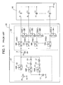
- Fig. 1 of the attached drawings shows part of a driver device that drives a capacitive display panel to emit light by applying a variety of drive pulses to the capacitive display panel.
- This driver device is disclosed in Japanese Patent Kokai (Laid-Open Application) No. 2002-156941.
- a PDP 10 has a plurality of row electrodes (not shown) and a plurality of column electrodes Z 1 to Z m arranged to intersect one another. Discharge cells (not shown), which correspond with pixels, are formed at the points of intersection between the row and column electrodes.
- a column electrode driver circuit 20 includes a power supply circuit 21, which generates a resonance pulse supply voltage in accordance with switching signals SW1 to SW3, and a pixel data pulse generation circuit 22, which generates a pixel data pulse applied to each of the column electrodes Z 1 to Z m on the basis of the resonance pulse supply voltage.
- the pixel data pulse generation circuit 22 includes switching elements SWZ 1 to SWZ m and SWZ 10 to SWZ m0 .
- the switching elements SWZ 1 to SWZ m and SWZ 10 to SWZ m0 are each controlled to become an ON state or an OFF state (turned on or off) individually in accordance with one display line's worth of (m) pixel data bits DB 1 to DB m that designate the states (lit or unlit) of the discharge cells on the basis of an inputted picture signal.
- Each of the switching elements SWZ 1 to SWZ m enters the ON state as long as the pixel data bit DB i supplied thereto is logic level 1, for example, and applies the resonance pulse supply voltage of the supply line 2 to the corresponding column electrode Z i (Z 1 to Z m ).
- the switching element SWZ i0 (SWZ 10 to SWZ m0 ) enters the ON state and applies the ground potential to the corresponding column electrode Z i (Z 1 to Z m ).
- Switching signals SW1 to SW3 which repeatedly set the switching elements S1 to S3 to the ON state in the order of the switching elements S1, S3, and then S2, are supplied to operate the power supply circuit 21.
- the capacitor C1 When only the switching element S1 enters the ON state in accordance with the switching signal SW1, the capacitor C1 is discharged and the discharge current thereof is released to the power supply line 2 via the coil L1 and diode D1. If the switching element SWZ i of the pixel data pulse generation circuit 22 is in the ON state, the discharge current flows into the column electrode Z i of the PDP 10 via the switching element SWZ i , the load capacitor C 0 that is parasitic on the column electrode Z i is charged, and an accumulation of electrical charge occurs within the load capacitor C 0 . Therefore, the potential of the power supply line 2 gradually rises because of the resonance action caused by the coil L1 and the load capacitor C 0 . This voltage increase is the rising edge of the high-voltage pixel data pulse.
- a power supply voltage Va generated by a DC power supply B1 is applied to the power supply line 2.
- the power supply voltage Va is the maximum voltage of the high-voltage pixel data pulse.
- the load capacitor C 0 that is parasitic on the column electrode Z i of the PDP 10 is discharged.
- the discharge current flows into the capacitor C1 via the column electrode Z i , the switching element SWZ i , the power supply line 2, the coil L2, the diode D2, and the switching element S2, whereby the capacitor C1 is charged. That is, the electrical charge that has accumulated in the load capacitor C 0 of the PDP 10 is gradually recovered by the capacitor C1 provided in the power supply circuit 21.
- the voltage of the power supply line 2 gradually drops in accordance with the time constant that is determined by the coil L2 and load capacitor C 0 . This decrease of the voltage is the trailing edge of the high-voltage pixel data pulse.
- the electrical charge that has accumulated in the PDP 10 as a capacitive load is recovered by the capacitor C1 and reused, whereby a reduced consumption of electrical power is achieved.
- the switching element SWZ 1 When the switching element SWZ 1 enters the ON state in response to the pixel data bit DB 1 of logic level 1, for example, the resonance pulse supply voltage, whose variation between the leading and trailing edges thereof is gradual and whose maximum voltage is Va, is supplied to the column electrode Z 1 as a high-voltage pixel data pulse.
- the switching element SWZ 10 when the pixel data bit DB 1 is logic level 0, the switching element SWZ 10 enters the ON state, and therefore a low-voltage (ground potential) pixel data pulse is applied to the column electrode Z 1 . Part of the electrical charge that has accumulated in the load capacitor C 0 of the PDP 10 is consumed via the current path including the column electrode Z 1 and switching element SWZ 10 .
- the switching element SWZ 1 is fixed in the ON state and the SWZ 10 in the OFF state during this interval.
- the resonance pulse supply voltage applied to the power supply line 2 maintains the maximum voltage Va but the resonance amplitude gradually decreases. This is equal to applying a DC power supply voltage to the power supply line 2 (DC drive state).
- a resonance circuit that includes the capacitor C1, coils L1 and L2 and the load capacitor C 0 of the PDP 10 enters the DC drive state and this creates the risk of a faulty operation due to the localized generation of heat, noise generation, and so forth.
- One object of the present invention is to provide a driver device for driving capacitive light emitting elements that can achieve size reduction, increased reliability and reduced electrical power consumption while heat radiation is suppressed.
- an improved driver device for driving a plurality of capacitive light emitting elements by applying a plurality of drive pulses to the capacitive light emitting elements via a plurality of drive electrodes in accordance with pixel data derived from an inputted picture signal.
- the driver device includes an electrical charge recovery circuit that has a capacitor, to one end of which a reference voltage is applied and a coil, one end of which is connected to the other end of the capacitor.
- the driver device also includes a plurality of electrical charge recovery switches provided for the drive electrodes respectively. Each electric charge recovery switch has a first switching element associated with one drive electrode to send a current corresponding with electrical charge that has accumulated in the capacitor to the associated drive electrode via the other end of the coil.
- Each electric charge recovery switch also has a second switching element that sends a current corresponding with electrical charge that has accumulated in the associated capacitive light emitting element to the other end of the coil via the associated drive electrode.
- the driver device also includes a plurality of output buffers provided for the drive electrodes respectively. Each output buffer has a third switching element that applies a predetermined high voltage to the associated drive electrode in accordance with the pixel data. Each output buffer also has a fourth switching element that applies the reference voltage to the associated drive electrode in accordance with the pixel data.
- the driver device also includes a drive control circuit that determines, for each of the drive electrodes, whether a voltage of the drive electrode concerned has shifted from the high voltage to the low voltage or from the low voltage to the high voltage on the basis of the pixel data.
- the drive control circuit sets either the first or second switching element of the electrical charge recovery switch associated with the drive electrode to the ON state over a predetermined period. If the voltage shift has not occurred on the drive electrode concerned, the drive control circuit sets the first and second switching elements of the electrical charge recovery switch associated with the drive electrode to the OFF state.
- a display device that adopts a PDP as a display panel having a plurality of capacitive light emitting elements will be described.
- a PDP 10 includes a plurality of row electrodes Y 1 to Y n and X 1 to X n , which are arranged to extend in the row (width) direction of the screen, and a plurality of column electrodes Z 1 to Z m , which are arranged to extend in the column (height) direction of the screen. Discharge spaces (not shown) are interposed between the row electrodes Y 1 to Y n and X 1 to X n and the column electrodes Z 1 to Z m .
- the row electrodes Y 1 to Y n and X 1 to X n are orthogonal to the column electrodes Z 1 to Z m .
- a single display line is defined by a pair of row electrodes X i and Y i . That is, n display lines consisting of first to nth display lines is formed in the PDP 10. Discharge cells are formed at the points of intersection between the display lines and the column electrodes Z. The discharge cells serve as pixels. That is, discharge cells corresponding with respective pixels are formed in the PDP 10 in the form of a matrix with n rows and m columns.
- a first row electrode driver circuit 30 generates a sustaining pulse, which allows only those discharge cells in which a wall charge remains to discharge, and applies the sustaining pulse to the row electrodes X 1 to X n of the PDP 10.
- a second row electrode driver circuit 40 generates a reset pulse, which initializes all the discharge cells, a scanning pulse, which sequentially selects one display line that becomes the pixel data write target, and a sustaining pulse, which allows only those discharge cells in which a wall charge remains to discharge. The second row electrode driver circuit 40 then applies these pulses to the row electrodes Y 1 to Y n .
- a drive control circuit 50 generates switching signals (as described later) SWH 1 to SWH m , SWL 1 to SWL m , SWU 1 to SWU m , and SWD 1 to SWD m on the basis of an inputted picture signal and supplies these switching signals to the column electrode driver circuit 200.
- the column electrode driver circuit 200 generates m pixel data pulses corresponding with the first to mth columns of the PDP 10 in accordance with the switching signals SWH 1 to SWH m , SWL 1 to SWL m , SWU 1 to SWU m , and SWD 1 to SWD m and applies these pixel data pulses to the column electrodes Z 1 to Z m of the PDP 10.
- the discharge cells belonging to the row electrode Y i to which the scanning pulse is applied are selectively discharged in accordance with the pixel data pulses. Specifically, those discharge cells to which the scanning pulse and a high-voltage pixel data pulse are applied are discharged, and other discharge cells to which the scanning pulse and a low-voltage pixel data pulse are applied are not discharged.
- each of the discharge cells is set to either a state where a wall charge is not present or a state where a wall charge remains.
- a sustaining pulse is applied by the row electrode driver circuits 30 and 40, only those discharge cells in which electrical charge remains are discharged to emit light.
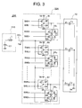
- Fig. 3 shows the internal configuration of the column electrode driver circuit 200.
- the column electrode driver 200 is the driver device of the present invention.
- the column electrode driver circuit 200 includes an electrical charge recovery circuit 210 and a pixel data pulse generation circuit 220.
- the electrical charge recovery circuit 210 has a capacitor C1 and an inductance coil L.
- One electrode of the capacitor C1 is grounded at the ground potential Vs of the PDP 10 and the other electrode is connected to one end of the coil L.
- the other end of the coil L is electrically connected via a discharge/charge line DCL to a discharge/charge terminal TM that is provided in the pixel data pulse generation circuit 220.
- the pixel data pulse generation circuit 220 includes m output buffers B 1 to B m corresponding with the column electrodes Z 1 to Z m of the PDP 10, m electrical charge recovery switches DS 1 to DS m , and the discharge/charge terminal TM.
- the terminal TM is an external terminal.
- Each of the output buffers B 1 to B m includes a p-channel-type MOS (Metal Oxide Semiconductor) transistor QP (referred to simply as 'transistor QP' hereinafter) and an n-channel-type MOS transistor QN (hereinafter referred to simply as 'transistor QN').
- the DC power supply voltage Va is applied to the source electrode of the transistor QP of each output buffer B i , and the source electrode of the transistor QN of each output buffer B i is grounded at ground potential Vs.
- the drain electrode of the transistor QP is connected to the drain electrode of the transistor QN, the node between these drain electrodes being the output terminal of the output buffer B i .
- the column electrode Z i (Z 1 to Z m ) is connected to the output terminal of the corresponding output buffer B i (B 1 to B m ).
- a switching signal SWH i is supplied to the gate electrode of the transistor QP of the corresponding output buffer B i .
- the switching signal SWH 1 is supplied to the gate electrode of the transistor QP of the output buffer B 1
- the switching signal SWH 2 is supplied to the gate electrode of the transistor QP of the output buffer B 2
- the switching signal SWH 3 is supplied to the gate electrode of the transistor QP of the output buffer B 3 .
- a switching signals SWL i is supplied to the gate electrode of the transistor QN of the corresponding output buffer B i .
- the switching signal SWL 1 is supplied to the gate electrode of the transistor QN of the output buffer B 1
- the switching signal SWL 2 is supplied to the gate electrode of the transistor QN of the output buffer B 2
- the switching signal SWL 3 is supplied to the gate electrode of the transistor QN of the output buffer B 3 .
- the output buffer B i applies the power supply voltage Va to the column electrode Z i of the PDP 10 via the output terminal of the output buffer B i .
- the output buffer B i applies the ground potential Vs to the column electrode Z i of the PDP 10 via the output terminal of the output buffer B i .
- Each of the electrical charge recovery switches DS 1 to DS m includes a p-channel-type MOS transistor QU (hereinafter referred to simply as 'transistor QU' ) and a p-channel-type MOS transistor QD (hereinafter referred to simply as 'transistor QD').
- the source electrodes S of the transistors QU and QD are connected to one another.
- the drain electrodes D of the transistors QD of the electrical charge recovery switches DS 1 to DS m are commonly connected to the discharge/charge terminal TM.
- the drain electrode D of the transistor QU of each electrical charge recovery switch DS i is connected to the corresponding column electrode Z i .
- the source electrodes S of the transistors QU and QD are connected to one another.
- the source electrode S of the transistor QU is also connected to an n-channel-type semiconductor formation region where the transistor QU is constructed, and the source electrode S of the transistor QD is also connected to an n-channel-type semiconductor formation region where the transistor QD is constructed.
- a switching signal SWU i is supplied to the gate electrode of the transistor QU in the corresponding electrical charge recovery switch DS i . That is, the switching signal SWU 1 is supplied to the gate electrode of the transistor QU of the electrical charge recovery switch DS 1 , the switching signal SWU 2 is supplied to the gate electrode of the transistor QU of the electrical charge recovery switch DS 2 , and the switching signal SWU 3 is supplied to the gate electrode of the transistor QU of the electrical charge recovery switch DS 3 .
- a switching signal SWD i is supplied to the gate electrode of the transistor QD in the corresponding electrical charge recovery switch DS i .
- the switching signal SWD 1 is supplied to the gate electrode of the transistor QD of the electrical charge recovery switch DS 1
- the switching signal SWD 2 is supplied to the gate electrode of the transistor QD of the electrical charge recovery switch DS 2
- the switching signal SWD 3 is supplied to the gate electrode of the transistor QD of the electrical charge recovery switch DS 3 .
- the drive control circuit 50 converts an inputted picture signal to 8-bit pixel data, for example, for each pixel and divides the pixel data into respective bit digits to obtain pixel data bits DB.
- the drive control circuit 50 determines, for each column, the logic level of each pixel data bit DB in the pixel data bit string in the order of the display lines.
- the pixel data bit string is a (vertical) string of pixel data bits DB with respect to the first to nth display lines that belong to the column concerned.
- the drive control circuit 50 determines whether the logic level has shifted from 0 to 1 or from 1 to 0.
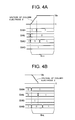
- the drive control circuit 50 determines that a shift from logic level 0 to 1 occurs, the drive control circuit 50 supplies the switching signals SWH, SWL, SWU and SWD that are indicated by the switching sequence S LH in Fig. 4A to the output buffer B and electrical charge recovery switch DS that belong to the column concerned.
- the transistors QP and QN of the output buffer B first both enter an OFF state in accordance with the logic-level-0 switching signal SWL and the logic-level-1 switching signal SWH.
- the transistors QD and QU of the electrical charge recovery switch DS enter the OFF state and ON state respectively in accordance with the logic-level-0 switching signal SWU and the logic-level-1 switching signal SWD.
- a current that corresponds with the electrical charge that has accumulated in the capacitor C1 of the electrical charge recovery circuit 210 flows into the column electrode Z via the coil L, discharge/charge terminal TM, the parasitic diode D1 that is parasitic across the drain and source of the transistor QD, and the transistor QU, whereby the load capacitor C 0 that is parasitic on the column electrode Z is charged. Therefore, under the resonance action of the coil L and load capacitor C 0 , the voltage of the column electrode Z gradually rises as shown in Fig. 4A. This voltage increase is the leading edge of the pixel data pulse. That is, the leading edge of the pixel data pulse is generated by using the electrical charge that has accumulated in the capacitor C1 of the electrical charge recovery circuit 210.
- the transistor QP of the output buffer B enters the ON state and the power supply voltage Va is applied directly to the column electrode Z.
- the power supply voltage Va is the maximum voltage value of the high-voltage pixel data pulse.
- the switching signal SWU switches from logic level 0 to logic level 1 and the transistors QD and QU of the electrical charge recovery switch DS both enter the OFF state.
- the release of the electrical charge from the capacitor C1 of the electrical charge recovery circuit 210 to the load capacitor C 0 of the PDP 10 ends.
- the drive control circuit 50 when it is determined that the logic level of the pixel data bit DB has shifted from 1 to 0, the drive control circuit 50 generates switching signals SWH, SWL, SWU and SWD as indicated by the switching sequence S HL of Fig. 4B.
- the transistors QP and QN of the output buffer B first both enter the OFF state in accordance with the logic-level-0 switching signal SWL and the logic-level-1 switching signal SWH.
- the transistors QU and QD of the electrical charge recovery switch DS enter the OFF state and the ON state respectively in accordance with the logic-level-0 switching signal SWD and logic-level-1 switching signal SWU.
- the trailing edge of the pixel data pulse is generated as a result of recovery of the electrical charge, that has accumulated in the load capacitor C 0 of the PDP 10, by the capacitor C1 of the electrical charge recovery circuit 210.
- the switching signal SWL shifts from logic level 0 to 1
- the transistor QN of the output buffer B enters the ON state and the column electrode Z is grounded at 0 volt.
- the 0 volt is the low-voltage pixel data pulse.
- the switching signal SWD switches from logic level 0 to logic level 1 and the transistors QD and QU of the electrical charge recovery switch DS both enter the OFF state. Accordingly, the electrical charge recovery from the load capacitor C 0 of the PDP 10 by the capacitor C1 of the electrical charge recovery circuit 210 ends.
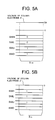
- the electrical charge recovery switches DS and output buffers B are controlled in accordance with the switching sequence S HH as shown in Fig. 5A.
- the transistors QD and QU of the electrical charge recovery switches DS both enter the OFF state and the transistors QP of the output buffers B enter the ON state, such that the power supply voltage Va is applied directly to the column electrodes Z. Because the transistors QD and QU of the electrical charge recovery switches DS are both in the OFF state, the electrical charge recovery is not effected by the electrical charge recovery circuit 210.
- the electrical charge recovery switches DS and output buffers B are controlled in accordance with the switching sequence S LL as shown in Fig. 5B.
- the transistors QD and QU of the electrical charge recovery switches DS both enter the OFF state and the transistors QN of the output buffers B enter the ON state, whereby the column electrodes Z are set at ground potential (0 volt).
- the drive control circuit 50 executes the above described drive individually with respect to the electrical charge recovery switches DS 1 to DS m and the output buffers B 1 to B m on the basis of the pixel data bits DB 1 to DB m that correspond with the first to mth columns of the PDP 10.
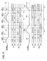
- Fig. 6 shows part of the operation based on the switching sequences S HL and S LH , which are carried out on the electrical charge recovery switches DS 1 and DS 2 and output buffers B 1 and B 2 associated with the column electrodes Z 1 and Z 2 respectively.
- the string of pixel data bits DB 1 which corresponds with the display lines belonging to the first column of the PDP 10
- the string of pixel data bits DB 2 which correspond with the respective display lines belonging to the second column, is '0,1,0,1'.
- the switching sequences S LH and S HL are executed alternately on the electrical charge recovery switch DS 2 and the output buffer B 2 as shown in Fig. 6.
- the low-voltage (0 volt) pixel data pulse DP L corresponding with a logic-level-0 pixel data bit DB 2 and the high-voltage (power supply voltage Va) pixel data pulse DP H corresponding with a logic-level-1 pixel data bit DB 2 are repeated alternately and applied to the column electrode Z 2 .
- the timing to shift the voltage of the column electrode Z 1 from a high voltage (power supply voltage Va) to a low voltage (0 volt) and the timing to shift the voltage of the column electrode Z 2 from a low voltage to a high voltage are shifted (offset) with respect to one another.
- the timing to shift the voltage of the column electrode Z 1 from a low voltage (0 volt) to a high voltage (power supply voltage Va) and the timing to shift the voltage of the column electrode Z 2 from a high voltage to a low voltage are shifted with respect to one another. That is, the drive control circuit 50 sets the transistor QU in one electrical charge recovery switch DS and the transistor QD in another electrical charge recovery switch DS to the ON state at different timings. Further, the drive control circuit 50 sets the transistor QD in one electrical charge recovery switch DS and the transistor QU in another electrical charge recovery switch DS to the ON state at different timings.
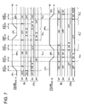
- the pulse width of the low-voltage pixel data pulse DP L is wider than that of the high-voltage pixel data pulse DP H in Fig. 6, the high-voltage pixel data pulse DP H may have a larger pulse width as shown in Fig. 7.
- the column electrode drive circuit 200 shown in Fig. 3 first determines, for each of the 1st to mth columns of the PDP 10, whether the logic level of each pixel data bit in a series of pixel data bits DB for the column concerned has shifted from 1 to 0 or from 0 to 1.
- the transistors QP and QN of the output buffer B associated with the column are both set to the OFF state.
- the electrical charge recovery operation switching sequence S HL or S LH ) by the electrical charge recovery circuit 210 is executed by setting the electrical charge recovery switch DS (either the transistor QU or QD) associated with the column to the ON state over a predetermined period. The leading and trailing edges of the pixel data pulse are generated by means of this electrical charge recovery operation. Then, the electrical charge recovery operation is terminated by setting the electrical charge recovery switch DS (both transistors QU and QD) to the OFF state.
- the transistor QP or QN of the output buffer B is set to the ON state in accordance with the pixel data bit DB, whereby the power supply voltage Va or 0 volt is applied directly to the column electrode Z over a predetermined interval.
- the electrical charge recovery operation switching sequence S HL or S LH ) by the charge recovery circuit 210 is executed by setting the electrical charge recovery switch DS (either transistor QU or QD) belonging to the column to the ON state once again, whereby the trailing edge or rising edge of the pixel data pulse is generated.
- the electrical charge recovery switch DS belonging to the column is always set to the OFF state. Meanwhile, by setting either the transistor QP or QN of the output buffer B to the ON state in accordance with the pixel data bit DB, the power supply voltage Va or 0 volt is applied to the column electrode Z directly (switching sequence S HH or S LL ).
- the column electrode drive circuit 200 shown in Fig. 3 first determines, for each column, whether the string of pixel data bits DB for the column concerned have successively the same logic level, so as to determine whether the voltage of the column electrode Z changes.
- the voltage of the column electrode Z changes from Va to 0 volt or from 0 volt to Va
- either the transistor QU or QD of the electrical charge recovery switch DS is set to the ON state so that the electrical charge recovery circuit 210 performs the electrical charge recovery, whereby the trailing edge or rising edge of the pixel data pulse is generated.
- both transistors QU and QD of the electrical charge recovery switch DS are always set to the OFF state so that the electrical charge recovery operation stops.
- the resonance circuit which includes the capacitor C1, coil L and load capacitor C 0 of the PDP 10, does not enter a DC drive state, and hence a faulty operation due to the localized heat generation and noises is prevented.
- the output buffers B 1 to B m and electrical charge recovery switches DS 1 to DS m are each an IC having a CMOS (Complementary Metal Oxide Semiconductor) structure and provided in the form of an IC package.
- the electrical charge recovery circuit 210 which includes two discrete components corresponding to the capacitor C1 and the coil L, is externally connected to the discharge/charge terminal TM of the IC package.
- the present invention is not limited to the illustrated and described embodiment.
- p-channel-type MOS transistors are adopted for the transistors QP, QU and QN in Fig. 3, n-channel-type transistors may be adopted.
- the drain electrode D of the transistor QU of each electrical charge recovery switch DS is connected to the corresponding column electrode Z and the drain electrode D of the transistor QD of each electrical charge recovery switch DS is connected to the discharge/charge terminal TM.
- the drain electrode D of the transistor QD may be connected to the column electrode Z and the drain electrode D of the transistor QU may be connected to the discharge/charge terminal TM.
- a predetermined time interval (discrepancy) is provided between the shift period for the column electrode Z 1 (trailing edge period) and the shift period for the column electrode Z 2 (leading edge period) and between the shift period for the column electrode Z 2 (trailing edge period) and the shift period for the column electrode Z 1 (leading edge period).
- this time interval is shortened as much as possible.
- the shift period for the column electrode Z 2 (leading edge period) is started immediately following completion of the shift period for the column electrode Z 1 (trailing edge period), and the shift period for the column electrode Z 1 (leading edge period) is started immediately following completion of the shift period (trailing edge period) for the column electrode Z 2 .
- the shift period for the column electrode Z 2 may be started immediately following completion of the shift period for the column electrode Z 1 (leading edge period), and the shift period for the column electrode Z 1 (trailing edge period) may be started immediately following completion of the shift period for the column electrode Z 2 (leading edge period).
Landscapes
- Engineering & Computer Science (AREA)
- Physics & Mathematics (AREA)
- Power Engineering (AREA)
- Plasma & Fusion (AREA)
- Computer Hardware Design (AREA)
- General Physics & Mathematics (AREA)
- Theoretical Computer Science (AREA)
- Control Of Indicators Other Than Cathode Ray Tubes (AREA)
- Control Of El Displays (AREA)
- Electroluminescent Light Sources (AREA)
- Control Of Gas Discharge Display Tubes (AREA)
- Electronic Switches (AREA)
Applications Claiming Priority (2)
| Application Number | Priority Date | Filing Date | Title |
|---|---|---|---|
| JP2003356034A JP2005121862A (ja) | 2003-10-16 | 2003-10-16 | 容量性発光素子の駆動装置 |
| JP2003356034 | 2003-10-16 |
Publications (2)
| Publication Number | Publication Date |
|---|---|
| EP1524643A2 true EP1524643A2 (fr) | 2005-04-20 |
| EP1524643A3 EP1524643A3 (fr) | 2009-01-21 |
Family
ID=34373590
Family Applications (1)
| Application Number | Title | Priority Date | Filing Date |
|---|---|---|---|
| EP04023950A Withdrawn EP1524643A3 (fr) | 2003-10-16 | 2004-10-07 | Dispositif pour commander des éléments luminescents capacitifs |
Country Status (4)
| Country | Link |
|---|---|
| US (1) | US7102597B2 (fr) |
| EP (1) | EP1524643A3 (fr) |
| JP (1) | JP2005121862A (fr) |
| KR (1) | KR100656720B1 (fr) |
Cited By (2)
| Publication number | Priority date | Publication date | Assignee | Title |
|---|---|---|---|---|
| EP1760681A1 (fr) * | 2005-08-31 | 2007-03-07 | LG Electronics Inc. | Appareil d'affichage à plasma, procédé de commande d'appareil d'affichage à plasma et module de circuit intégré à commande par adresse |
| EP1927972A3 (fr) * | 2006-11-29 | 2009-08-19 | LG Electronics Inc. | Appareil d'affichage à plasma |
Families Citing this family (7)
| Publication number | Priority date | Publication date | Assignee | Title |
|---|---|---|---|---|
| JP5048943B2 (ja) * | 2005-12-13 | 2012-10-17 | パナソニック株式会社 | 容量性発光素子の駆動装置 |
| JP5021932B2 (ja) * | 2005-12-15 | 2012-09-12 | パナソニック株式会社 | 表示パネルの駆動装置 |
| KR100765506B1 (ko) * | 2006-05-04 | 2007-10-10 | 엘지전자 주식회사 | 플라즈마 디스플레이 장치 |
| KR20080108794A (ko) * | 2007-06-11 | 2008-12-16 | 엘지전자 주식회사 | 플라즈마 디스플레이 장치 및 그의 구동방법 |
| WO2009004685A1 (fr) | 2007-06-29 | 2009-01-08 | Hitachi, Ltd. | Procédé permettant de commander un panneau d'écran plasma et dispositif d'affichage plasma |
| JP5432158B2 (ja) * | 2008-09-10 | 2014-03-05 | 日立コンシューマエレクトロニクス株式会社 | プラズマディスプレイ装置 |
| CN114242017B (zh) * | 2021-12-23 | 2023-08-01 | 惠州视维新技术有限公司 | 一种显示面板及其驱动方法、显示装置 |
Family Cites Families (10)
| Publication number | Priority date | Publication date | Assignee | Title |
|---|---|---|---|---|
| EP0644505B1 (fr) * | 1993-09-17 | 2000-03-08 | Hitachi, Ltd. | Dispositif d'affichage avec agencement d'entrée de coordonnées |
| JP2795191B2 (ja) * | 1994-10-04 | 1998-09-10 | 株式会社デンソー | El表示装置の駆動装置 |
| JP3241577B2 (ja) * | 1995-11-24 | 2001-12-25 | 日本電気株式会社 | 表示パネル駆動回路 |
| JP3006534B2 (ja) | 1997-03-31 | 2000-02-07 | 日本電気株式会社 | 半導体装置 |
| US6329980B1 (en) * | 1997-03-31 | 2001-12-11 | Sanjo Electric Co., Ltd. | Driving circuit for display device |
| JP2000098974A (ja) * | 1998-09-24 | 2000-04-07 | Pioneer Electronic Corp | 容量性発光素子ディスプレイ装置及びその駆動方法 |
| JP3656805B2 (ja) * | 1999-01-22 | 2005-06-08 | パイオニア株式会社 | 温度補償機能を有する有機el素子駆動装置 |
| KR100490532B1 (ko) * | 2000-04-28 | 2005-05-17 | 삼성에스디아이 주식회사 | 어드레스 전극 구동 전력 회수 회로를 갖는 플라즈마표시패널의 구동장치 |
| JP4660026B2 (ja) | 2000-09-08 | 2011-03-30 | パナソニック株式会社 | 表示パネルの駆動装置 |
| CN1639761A (zh) * | 2002-03-06 | 2005-07-13 | 皇家飞利浦电子股份有限公司 | 具有能量回收系统的显示板 |
-
2003
- 2003-10-16 JP JP2003356034A patent/JP2005121862A/ja active Pending
-
2004
- 2004-10-07 EP EP04023950A patent/EP1524643A3/fr not_active Withdrawn
- 2004-10-13 US US10/962,531 patent/US7102597B2/en not_active Expired - Fee Related
- 2004-10-16 KR KR1020040082914A patent/KR100656720B1/ko not_active Expired - Fee Related
Cited By (3)
| Publication number | Priority date | Publication date | Assignee | Title |
|---|---|---|---|---|
| EP1760681A1 (fr) * | 2005-08-31 | 2007-03-07 | LG Electronics Inc. | Appareil d'affichage à plasma, procédé de commande d'appareil d'affichage à plasma et module de circuit intégré à commande par adresse |
| EP1927972A3 (fr) * | 2006-11-29 | 2009-08-19 | LG Electronics Inc. | Appareil d'affichage à plasma |
| US8081143B2 (en) | 2006-11-29 | 2011-12-20 | Lg Electronics Inc. | Plasma display apparatus |
Also Published As
| Publication number | Publication date |
|---|---|
| US20050083257A1 (en) | 2005-04-21 |
| US7102597B2 (en) | 2006-09-05 |
| KR100656720B1 (ko) | 2006-12-12 |
| EP1524643A3 (fr) | 2009-01-21 |
| JP2005121862A (ja) | 2005-05-12 |
| KR20050036829A (ko) | 2005-04-20 |
Similar Documents
| Publication | Publication Date | Title |
|---|---|---|
| JP5015380B2 (ja) | Pdpのエネルギー回収装置及びその方法と、それを利用した高速アドレッシング方法 | |
| US20040104866A1 (en) | Capacitive load drive recovery circuit, capacitive load drive circuit and plasma display apparatus using the same | |
| EP1365380A2 (fr) | Circuit d'attaque pour charge capacitive et appareil d' affichage à plasma | |
| EP1139323A2 (fr) | Dispositif d'affichage à plasma et méthode de fabrication | |
| US20050168410A1 (en) | Drive circuit and drive method | |
| US6211865B1 (en) | Driving apparatus of plasma display panel | |
| US7102597B2 (en) | Driver device for driving capacitive light emitting elements | |
| US7136032B2 (en) | Plasma display apparatus | |
| KR20040089465A (ko) | 용량성 부하 구동 회로 및 플라즈마 디스플레이 장치 | |
| JP3556108B2 (ja) | Pdpの駆動方法 | |
| KR100330032B1 (ko) | 플라즈마 디스플레이 패널의 전력회수장치 및 이를 이용한고속 어드레싱 방법 | |
| US7768474B2 (en) | Device for driving capacitive light emitting element | |
| US6882330B2 (en) | Field emission displaying device and driving method thereof | |
| KR100709938B1 (ko) | 용량성 발광소자의 구동장치 | |
| JP4955956B2 (ja) | 駆動回路および表示装置 | |
| KR100505981B1 (ko) | 전력회수장치 및 전력회수방법 | |
| EP1202240A1 (fr) | Procede d'entrainement d'un panneau d'affichage | |
| EP1684259A2 (fr) | Dispositif de commande d'un panneau d'affichage comprenant des éléments électroluminescents capacitifs | |
| JP2007128021A (ja) | プラズマディスプレイ駆動装置及びその駆動方法 | |
| KR20010031929A (ko) | 전계 방출 표시기의 구동회로 | |
| JP2009122341A (ja) | プラズマディスプレイ装置 | |
| KR20000019415A (ko) | 전계 방출 표시기의 게이트 구동회로 | |
| JP2004157553A (ja) | プラズマディスプレイ装置の製造方法 | |
| JP2007163788A (ja) | 容量性発光素子の駆動装置 |
Legal Events
| Date | Code | Title | Description |
|---|---|---|---|
| PUAI | Public reference made under article 153(3) epc to a published international application that has entered the european phase |
Free format text: ORIGINAL CODE: 0009012 |
|
| AK | Designated contracting states |
Kind code of ref document: A2 Designated state(s): AT BE BG CH CY CZ DE DK EE ES FI FR GB GR HU IE IT LI LU MC NL PL PT RO SE SI SK TR |
|
| AX | Request for extension of the european patent |
Extension state: AL HR LT LV MK |
|
| PUAL | Search report despatched |
Free format text: ORIGINAL CODE: 0009013 |
|
| AK | Designated contracting states |
Kind code of ref document: A3 Designated state(s): AT BE BG CH CY CZ DE DK EE ES FI FR GB GR HU IE IT LI LU MC NL PL PT RO SE SI SK TR |
|
| AX | Request for extension of the european patent |
Extension state: AL HR LT LV MK |
|
| AKX | Designation fees paid |
Designated state(s): DE FR GB |
|
| STAA | Information on the status of an ep patent application or granted ep patent |
Free format text: STATUS: THE APPLICATION IS DEEMED TO BE WITHDRAWN |
|
| 18D | Application deemed to be withdrawn |
Effective date: 20090722 |