EP1521295A2 - Méthode de fabrication d'une succession de couches épitaxiales d'un composant et puce optoélectronique semiconductrice - Google Patents
Méthode de fabrication d'une succession de couches épitaxiales d'un composant et puce optoélectronique semiconductrice Download PDFInfo
- Publication number
- EP1521295A2 EP1521295A2 EP04022980A EP04022980A EP1521295A2 EP 1521295 A2 EP1521295 A2 EP 1521295A2 EP 04022980 A EP04022980 A EP 04022980A EP 04022980 A EP04022980 A EP 04022980A EP 1521295 A2 EP1521295 A2 EP 1521295A2
- Authority
- EP
- European Patent Office
- Prior art keywords
- layer
- iii
- compound semiconductor
- semiconductor material
- substrate
- Prior art date
- Legal status (The legal status is an assumption and is not a legal conclusion. Google has not performed a legal analysis and makes no representation as to the accuracy of the status listed.)
- Granted
Links
Images
Classifications
-
- C—CHEMISTRY; METALLURGY
- C30—CRYSTAL GROWTH
- C30B—SINGLE-CRYSTAL GROWTH; UNIDIRECTIONAL SOLIDIFICATION OF EUTECTIC MATERIAL OR UNIDIRECTIONAL DEMIXING OF EUTECTOID MATERIAL; REFINING BY ZONE-MELTING OF MATERIAL; PRODUCTION OF A HOMOGENEOUS POLYCRYSTALLINE MATERIAL WITH DEFINED STRUCTURE; SINGLE CRYSTALS OR HOMOGENEOUS POLYCRYSTALLINE MATERIAL WITH DEFINED STRUCTURE; AFTER-TREATMENT OF SINGLE CRYSTALS OR A HOMOGENEOUS POLYCRYSTALLINE MATERIAL WITH DEFINED STRUCTURE; APPARATUS THEREFOR
- C30B25/00—Single-crystal growth by chemical reaction of reactive gases, e.g. chemical vapour-deposition growth
- C30B25/02—Epitaxial-layer growth
-
- C—CHEMISTRY; METALLURGY
- C30—CRYSTAL GROWTH
- C30B—SINGLE-CRYSTAL GROWTH; UNIDIRECTIONAL SOLIDIFICATION OF EUTECTIC MATERIAL OR UNIDIRECTIONAL DEMIXING OF EUTECTOID MATERIAL; REFINING BY ZONE-MELTING OF MATERIAL; PRODUCTION OF A HOMOGENEOUS POLYCRYSTALLINE MATERIAL WITH DEFINED STRUCTURE; SINGLE CRYSTALS OR HOMOGENEOUS POLYCRYSTALLINE MATERIAL WITH DEFINED STRUCTURE; AFTER-TREATMENT OF SINGLE CRYSTALS OR A HOMOGENEOUS POLYCRYSTALLINE MATERIAL WITH DEFINED STRUCTURE; APPARATUS THEREFOR
- C30B29/00—Single crystals or homogeneous polycrystalline material with defined structure characterised by the material or by their shape
- C30B29/10—Inorganic compounds or compositions
- C30B29/40—AIIIBV compounds wherein A is B, Al, Ga, In or Tl and B is N, P, As, Sb or Bi
-
- H—ELECTRICITY
- H10—SEMICONDUCTOR DEVICES; ELECTRIC SOLID-STATE DEVICES NOT OTHERWISE PROVIDED FOR
- H10P—GENERIC PROCESSES OR APPARATUS FOR THE MANUFACTURE OR TREATMENT OF DEVICES COVERED BY CLASS H10
- H10P14/00—Formation of materials, e.g. in the shape of layers or pillars
- H10P14/20—Formation of materials, e.g. in the shape of layers or pillars of semiconductor materials
- H10P14/29—Formation of materials, e.g. in the shape of layers or pillars of semiconductor materials characterised by the substrates
- H10P14/2901—Materials
- H10P14/2907—Materials being Group IIIA-VA materials
- H10P14/2911—Arsenides
-
- H—ELECTRICITY
- H10—SEMICONDUCTOR DEVICES; ELECTRIC SOLID-STATE DEVICES NOT OTHERWISE PROVIDED FOR
- H10P—GENERIC PROCESSES OR APPARATUS FOR THE MANUFACTURE OR TREATMENT OF DEVICES COVERED BY CLASS H10
- H10P14/00—Formation of materials, e.g. in the shape of layers or pillars
- H10P14/20—Formation of materials, e.g. in the shape of layers or pillars of semiconductor materials
- H10P14/32—Formation of materials, e.g. in the shape of layers or pillars of semiconductor materials characterised by intermediate layers between substrates and deposited layers
- H10P14/3202—Materials thereof
- H10P14/3214—Materials thereof being Group IIIA-VA semiconductors
- H10P14/3218—Phosphides
-
- H—ELECTRICITY
- H10—SEMICONDUCTOR DEVICES; ELECTRIC SOLID-STATE DEVICES NOT OTHERWISE PROVIDED FOR
- H10P—GENERIC PROCESSES OR APPARATUS FOR THE MANUFACTURE OR TREATMENT OF DEVICES COVERED BY CLASS H10
- H10P14/00—Formation of materials, e.g. in the shape of layers or pillars
- H10P14/20—Formation of materials, e.g. in the shape of layers or pillars of semiconductor materials
- H10P14/32—Formation of materials, e.g. in the shape of layers or pillars of semiconductor materials characterised by intermediate layers between substrates and deposited layers
- H10P14/3202—Materials thereof
- H10P14/3214—Materials thereof being Group IIIA-VA semiconductors
- H10P14/3221—Arsenides
-
- H—ELECTRICITY
- H10—SEMICONDUCTOR DEVICES; ELECTRIC SOLID-STATE DEVICES NOT OTHERWISE PROVIDED FOR
- H10P—GENERIC PROCESSES OR APPARATUS FOR THE MANUFACTURE OR TREATMENT OF DEVICES COVERED BY CLASS H10
- H10P14/00—Formation of materials, e.g. in the shape of layers or pillars
- H10P14/20—Formation of materials, e.g. in the shape of layers or pillars of semiconductor materials
- H10P14/32—Formation of materials, e.g. in the shape of layers or pillars of semiconductor materials characterised by intermediate layers between substrates and deposited layers
- H10P14/3242—Structure
- H10P14/3244—Layer structure
- H10P14/3251—Layer structure consisting of three or more layers
-
- H—ELECTRICITY
- H10—SEMICONDUCTOR DEVICES; ELECTRIC SOLID-STATE DEVICES NOT OTHERWISE PROVIDED FOR
- H10P—GENERIC PROCESSES OR APPARATUS FOR THE MANUFACTURE OR TREATMENT OF DEVICES COVERED BY CLASS H10
- H10P14/00—Formation of materials, e.g. in the shape of layers or pillars
- H10P14/20—Formation of materials, e.g. in the shape of layers or pillars of semiconductor materials
- H10P14/32—Formation of materials, e.g. in the shape of layers or pillars of semiconductor materials characterised by intermediate layers between substrates and deposited layers
- H10P14/3242—Structure
- H10P14/3244—Layer structure
- H10P14/3251—Layer structure consisting of three or more layers
- H10P14/3252—Alternating layers, e.g. superlattice
-
- H—ELECTRICITY
- H10—SEMICONDUCTOR DEVICES; ELECTRIC SOLID-STATE DEVICES NOT OTHERWISE PROVIDED FOR
- H10P—GENERIC PROCESSES OR APPARATUS FOR THE MANUFACTURE OR TREATMENT OF DEVICES COVERED BY CLASS H10
- H10P14/00—Formation of materials, e.g. in the shape of layers or pillars
- H10P14/20—Formation of materials, e.g. in the shape of layers or pillars of semiconductor materials
- H10P14/34—Deposited materials, e.g. layers
- H10P14/3402—Deposited materials, e.g. layers characterised by the chemical composition
- H10P14/3414—Deposited materials, e.g. layers characterised by the chemical composition being group IIIA-VIA materials
- H10P14/3418—Phosphides
-
- H—ELECTRICITY
- H10—SEMICONDUCTOR DEVICES; ELECTRIC SOLID-STATE DEVICES NOT OTHERWISE PROVIDED FOR
- H10H—INORGANIC LIGHT-EMITTING SEMICONDUCTOR DEVICES HAVING POTENTIAL BARRIERS
- H10H20/00—Individual inorganic light-emitting semiconductor devices having potential barriers, e.g. light-emitting diodes [LED]
- H10H20/01—Manufacture or treatment
- H10H20/011—Manufacture or treatment of bodies, e.g. forming semiconductor layers
- H10H20/013—Manufacture or treatment of bodies, e.g. forming semiconductor layers having light-emitting regions comprising only Group III-V materials
Definitions
- the invention relates to a method for manufacturing an epitaxial device layer sequence on the base a first III / V compound semiconductor material system with a first group V element on a substrate or a Buffer layer, the or a material based on a second III / V compound semiconductor material system having a second group V element, that of the first group V element is different. It continues to refer to one corresponding optoelectronic semiconductor chip.
- the group of optoelectronic, ie radiation-emitting and / or radiation-detecting semiconductor chips based on InGaAlP in particular includes chips in which the epitaxially produced radiation-generating semiconductor layer sequence, which as a rule has a layer sequence of different individual layers, contains at least one single layer Material of the III-V compound semiconductor material system In x Al y Ga 1-xy P with 0 ⁇ x ⁇ 1, 0 ⁇ y ⁇ 1 and x + y ⁇ 1.
- the semiconductor layer sequence can, for example, have a conventional pn junction, a double heterostructure, a single quantum well structure (SQW structure) or a multiple quantum well structure (MQW structure). Such structures are known to the person skilled in the art and are therefore not explained in detail at this point.
- the present invention is based on the object Specify method of the type mentioned, with the Influence of substrate quality, especially on the optical and electrical qualities of the component layer sequence as well the aging stability can be reduced. Farther to specify a corresponding optoelectronic semiconductor chip become.
- the method is applied to the substrate or to the buffer layer before applying the epitaxial device layer sequence at least one layer sequence with a first and a second III / V compound semiconductor material layer applied.
- the first and second III / V compound semiconductor material layers show each other various compositions and contain both the first as well as the second group V element. This is preferred a rampant transition from growth to that with the second group V element is stabilized, to growth, which is stabilized with the first group V element generated.
- concentration of the second group V element within the first and second layers from the substrate Seen direction active layer sequence decreases continuously and the concentration of the first group V element continuously increases.
- the Konzentratinos stanos stanos stanos stanos stanos stanos stanos stanos the first and second group V-elements can be continuous or in stages run. Furthermore, the concentration of the first Group V-Elements do not force to the same extent from the substrate towards the active layer sequence increase, as the concentration of the second group V element decreases in this direction.
- the first III / V compound semiconductor material layer (s) comprises a quinternary composition
- the second III / V compound semiconductor material layer (s) an quinternary, quaternary, or ternary composition on (these can in several first III / V compound semiconductor material layers also different be).
- the method is preferably suitable for producing semiconductor chips in which the substrate is a GaAs substrate or a GaAs-based substrate, the component layer sequence is an In x Ga y Al 1 -xy P-based III / V compound semiconductor layer sequence with 0 ⁇ x ⁇ 1, 0 ⁇ y ⁇ 1 and x + y ⁇ 1 and the first and second III / V compound semiconductor material layers In x Ga y Al 1-xy As z P 1-z layers 0 ⁇ x ⁇ 1, 0 ⁇ y ⁇ 1; x + y ⁇ 1 and 0 ⁇ z ⁇ 1.
- a plurality of layer sequences is then provided, each layer sequence being an In x Ga y Al 1-xy As z P 1 -z layer with 0 ⁇ x ⁇ 1, 0 ⁇ y ⁇ 1; x + y ⁇ 1 and 0 ⁇ z ⁇ 1 and a GaAs z P 1-z layer with 0 ⁇ z ⁇ 1 or from an In x Ga y Al 1-xy As z P 1-z layer with 0 ⁇ x ⁇ 1, 0 ⁇ y ⁇ 1; x + y ⁇ 1 and 0 ⁇ z ⁇ 1 and a GaAs z P 1 -z layer with 0 ⁇ z ⁇ 1.
- the method is furthermore preferably suitable for the production of semiconductor chips in which the substrate is a GaAs substrate or a GaAs-based substrate, the component layer sequence is an In x Ga y Al 1 -xy P-based III / V compound semiconductor layer sequence with 0 ⁇ x ⁇ 1, 0 ⁇ y ⁇ 1 and x + y ⁇ 1, and the first (n) III / V compound semiconductor material layer (s) quinternary In x Ga y Al 1-xy As z P 1-z layers with 0 ⁇ x ⁇ 1, 0 ⁇ y ⁇ 1; x + y ⁇ 1 and 0 ⁇ z ⁇ 1 and the second III / V compound semiconductor material layer (s) are In x Ga y Al 1-xy As z P 1-z quaternary layers where 0 ⁇ x ⁇ 1, 0 ⁇ y ⁇ 1; x + y ⁇ 1 and 0 ⁇ z ⁇ 1.
- the layer thicknesses of the first and the second III / V compound semiconductor material layer (s) are preferably between 1 nm and 50 nm inclusive.
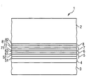
- the figure shows a schematic sectional view of a Semiconductor chips produced by a method according to the invention is made.
- the layer thicknesses shown in the embodiment are not to be considered as true to scale. Rather, they are for better understanding exaggeratedly thick and not with the actual Thickness ratios shown to each other.
- the semiconductor chip according to FIG. 1 is a Laser diode chip 1 with a laser-active component layer sequence 2 based on InGaAlP, on a one GaAs substrate 3 has grown epitaxially.
- an n-doped GaAs buffer layer is first applied to the substrate 3 4 epitaxially grown, on the following four layer pairs (layer sequences) 5,6,7,8 with one each n-doped InGaAlAsP layer 51, 61, 71, 81 (thickness, for example 20 nm each) and in each case one n-doped GaAsP layer 52.62, 72.82 (thickness, for example, 4 nm each) epitaxially grown up in such a way that in the Layer the InGaAlAsP layers and GaAsP layers together alternate.
- the P content can be in the layer pairs in the direction from the substrate to the component layer sequence towards the As content, at least on average.
- the n-type GaAs buffer layer 4 may be provided following also four layer pairs (layer sequences) 5,6,7,8 each with an n-doped InGaAlAsP layer 51,61,71,81 and each of an n-doped GaAlAsP layer 52,62,72,82 epitaxially to be raised.
- MOVPE metalorganic vapor phase epitaxy
- both Group V elements in addition to a targeted installation of foreign atoms (mitmigrierenden on the growth front) at the heterointerfaces by the In content dislocation defects intercepted and through the deliberate mixture of both Group V elements increase the crystal and interface quality.
- phosphorus in the layer pairs 5,6,7,8 may be a subsidence caused by the In content the band edge can be compensated for the electrical conductivity to increase the layer pairs and prevent absorption.
- Through a targeted tension of the layer pairs (superlattice) can a desired tension of the entire component structure be set.
- the mixture of both Group V elements is a ramp-like transition from here As-stabilized to P-stabilized growth.
- the invention is not specific to that described embodiments, but extends to all processes and semiconductor chips, the have the basic features of the invention. Especially the invention is basically applicable to all III / V compound semiconductor material systems but also on II / VI-. Compound semiconductor material systems applicable.
Landscapes
- Chemical & Material Sciences (AREA)
- Engineering & Computer Science (AREA)
- Crystallography & Structural Chemistry (AREA)
- Materials Engineering (AREA)
- Metallurgy (AREA)
- Organic Chemistry (AREA)
- Chemical Kinetics & Catalysis (AREA)
- General Chemical & Material Sciences (AREA)
- Inorganic Chemistry (AREA)
- Semiconductor Lasers (AREA)
Applications Claiming Priority (4)
| Application Number | Priority Date | Filing Date | Title |
|---|---|---|---|
| DE10345413A DE10345413A1 (de) | 2003-09-30 | 2003-09-30 | Verfahren zum Herstellen einer epitaktischen Bauelementschichtenfolge und optoelektronischer Halbleiterchip |
| DE10345413 | 2003-09-30 | ||
| DE10361659A DE10361659A1 (de) | 2003-12-30 | 2003-12-30 | Verfahrem zum Herstellen einer epitaktischen Bauelementschichtenfolge und optoelektronischer Halbleiterchip |
| DE10361659 | 2003-12-30 |
Publications (3)
| Publication Number | Publication Date |
|---|---|
| EP1521295A2 true EP1521295A2 (fr) | 2005-04-06 |
| EP1521295A3 EP1521295A3 (fr) | 2009-06-24 |
| EP1521295B1 EP1521295B1 (fr) | 2016-11-02 |
Family
ID=34315001
Family Applications (1)
| Application Number | Title | Priority Date | Filing Date |
|---|---|---|---|
| EP04022980.9A Expired - Lifetime EP1521295B1 (fr) | 2003-09-30 | 2004-09-27 | Méthode de fabrication d'une succession de couches épitaxiales d'un composant et puce optoélectronique semiconductrice |
Country Status (3)
| Country | Link |
|---|---|
| US (1) | US7317202B2 (fr) |
| EP (1) | EP1521295B1 (fr) |
| JP (1) | JP2005109507A (fr) |
Families Citing this family (3)
| Publication number | Priority date | Publication date | Assignee | Title |
|---|---|---|---|---|
| DE102005047152A1 (de) * | 2005-09-30 | 2007-04-12 | Osram Opto Semiconductors Gmbh | Epitaxiesubstrat, Verfahren zu seiner Herstellung und Verfahren zur Herstellung eines Halbleiterchips |
| DE102005056950A1 (de) * | 2005-09-30 | 2007-04-05 | Osram Opto Semiconductors Gmbh | Halbleitersubstrat aus GaAs und Halbleiterbauelement |
| ES2349610B1 (es) * | 2009-03-06 | 2011-07-21 | Pacific Speed Limited | Oblea epitaxial de semiconductor compuesto y metodo de fabricacion de la misma. |
Family Cites Families (8)
| Publication number | Priority date | Publication date | Assignee | Title |
|---|---|---|---|---|
| US4148045A (en) | 1977-09-21 | 1979-04-03 | International Business Machines Corporation | Multicolor light emitting diode array |
| US5048036A (en) * | 1989-09-18 | 1991-09-10 | Spectra Diode Laboratories, Inc. | Heterostructure laser with lattice mismatch |
| DE4011145A1 (de) | 1990-04-06 | 1991-10-10 | Telefunken Electronic Gmbh | Lumineszenz-halbleiterelement |
| JPH0766455A (ja) * | 1993-08-24 | 1995-03-10 | Shin Etsu Handotai Co Ltd | 半導体発光装置 |
| JP2914210B2 (ja) * | 1995-03-07 | 1999-06-28 | 日本電気株式会社 | 多重量子井戸構造光半導体装置及びその製造方法 |
| US6603784B1 (en) | 1998-12-21 | 2003-08-05 | Honeywell International Inc. | Mechanical stabilization of lattice mismatched quantum wells |
| US6542528B1 (en) * | 1999-02-15 | 2003-04-01 | Ricoh Company, Ltd. | Light-emitting semiconductor device producing red wavelength optical radiation |
| US6628694B2 (en) | 2001-04-23 | 2003-09-30 | Agilent Technologies, Inc. | Reliability-enhancing layers for vertical cavity surface emitting lasers |
-
2004
- 2004-09-27 EP EP04022980.9A patent/EP1521295B1/fr not_active Expired - Lifetime
- 2004-09-28 US US10/952,154 patent/US7317202B2/en not_active Expired - Lifetime
- 2004-09-30 JP JP2004288292A patent/JP2005109507A/ja not_active Withdrawn
Also Published As
| Publication number | Publication date |
|---|---|
| US7317202B2 (en) | 2008-01-08 |
| EP1521295A3 (fr) | 2009-06-24 |
| EP1521295B1 (fr) | 2016-11-02 |
| JP2005109507A (ja) | 2005-04-21 |
| US20050116242A1 (en) | 2005-06-02 |
Similar Documents
| Publication | Publication Date | Title |
|---|---|---|
| DE69838410T2 (de) | Herstellungsverfahren einer optischen Halbleitervorrichtung | |
| DE112004001447B4 (de) | Nitridhalbleiter-Licht-emittierende Einrichtung | |
| DE19725578B4 (de) | Reduzierung der Rißbildung im Material von III-V-Nitrid-Halbleiterbauelementen bei gleichzeitiger Maximierung der elektrischen Dotierung | |
| DE19905517B4 (de) | Mehrschichtige Indium-enthaltende Nitridpufferschicht für die Nitrid-Epitaxie | |
| EP1314209A1 (fr) | Procede pour produire une puce a semi-conducteur photoemettrice a base de semi-conducteur nitrure iii-v et puce a semi-conducteur photoemettrice correspondante | |
| DE10213358A1 (de) | Indiumgalliumnitrid-Glättungsstrukturen für III-Nitrid-Anordnungen | |
| DE10213395A1 (de) | Indiumgalliumnitrid-Glättungsstrukturen für III-Nitried-Anordnungen | |
| DE112012001920B4 (de) | Strahlung emittierender Halbleiterchip mit integriertem ESD-Schutz | |
| DE112013004996T5 (de) | Halbleitervorrichtung und Verfahren zu deren Herstellung | |
| EP2248192A1 (fr) | Corps semi-conducteur optoelectronique avec jonction a effet tunnel et procede de fabrication associe | |
| EP2208240A1 (fr) | Microplaquette semi-conductrice optoélectronique à structure de puits quantiques multiples | |
| DE102005005635A1 (de) | Strahlungsemittierendes optoelektronisches Bauelement mit einer Quantentopfstruktur und Verfahren zu dessen Herstellung | |
| WO2015011155A1 (fr) | Puce semi-conductrice optoélectronique pourvue d'un puits quantique multiple présentant au moins une couche barrière haute protection | |
| DE112014002691T5 (de) | Anregungsbereich, der Nanopunkte (auch als "Quantenpunkte" bezeichnet) in einem Matrixkristall umfasst, der auf Si-Substrat gezüchtet wurde und aus AlyInxGa1-y-xN-Kristall (y ≧ 0, x > 0) mit Zinkblendestruktur (auch als "kubisch" bezeichnet) besteht, und lichtemittierende Vorrichtung (LED und LD), die unter Verwendung desselben erhalten wurde | |
| WO2004057680A1 (fr) | Corps a semiconducteur emetteur de rayonnement et procede de production dudit corps | |
| DE69925547T2 (de) | Herstellung der Endflächen von Laserdioden durch Epitaxie auf Basis von III-V Materialien | |
| EP1521295B1 (fr) | Méthode de fabrication d'une succession de couches épitaxiales d'un composant et puce optoélectronique semiconductrice | |
| DE102009004895A1 (de) | Optoelektronisches Halbleiterbauelement | |
| DE19954242B4 (de) | Lichtemittierende Vorrichtung aus einem Nitridhalbleiter der Gruppe III | |
| EP1770767B1 (fr) | Substrat semiconducteur à GaAs et dispositif semiconducteur | |
| DE10056475B4 (de) | Strahlungsemittierendes Halbleiterbauelement auf GaN-Basis mit verbesserter p-Leitfähigkeit und Verfahren zu dessen Herstellung | |
| DE10361659A1 (de) | Verfahrem zum Herstellen einer epitaktischen Bauelementschichtenfolge und optoelektronischer Halbleiterchip | |
| DE10043938B4 (de) | Quantenmulden-Einrichtung mit ESD-Festigkeit und Verfahren zum Herstellen der Einrichtung | |
| DE102005037022A1 (de) | Strahlungsemittierender optoelektronischer Halbleiterchip mit einer Diffusionsbarriere | |
| DE10239045A1 (de) | Verfahren zum Herstellen eines elektromagnetische Strahlung emittierenden Halbleiterchips und elektromagnetische Strahlung emittierender Halbleiterchip |
Legal Events
| Date | Code | Title | Description |
|---|---|---|---|
| PUAI | Public reference made under article 153(3) epc to a published international application that has entered the european phase |
Free format text: ORIGINAL CODE: 0009012 |
|
| AK | Designated contracting states |
Kind code of ref document: A2 Designated state(s): AT BE BG CH CY CZ DE DK EE ES FI FR GB GR HU IE IT LI LU MC NL PL PT RO SE SI SK TR |
|
| AX | Request for extension of the european patent |
Extension state: AL HR LT LV MK |
|
| RAP1 | Party data changed (applicant data changed or rights of an application transferred) |
Owner name: OSRAM OPTO SEMICONDUCTORS GMBH |
|
| RAP1 | Party data changed (applicant data changed or rights of an application transferred) |
Owner name: OSRAM OPTO SEMICONDUCTORS GMBH |
|
| PUAL | Search report despatched |
Free format text: ORIGINAL CODE: 0009013 |
|
| AK | Designated contracting states |
Kind code of ref document: A3 Designated state(s): AT BE BG CH CY CZ DE DK EE ES FI FR GB GR HU IE IT LI LU MC NL PL PT RO SE SI SK TR |
|
| AX | Request for extension of the european patent |
Extension state: AL HR LT LV MK |
|
| 17P | Request for examination filed |
Effective date: 20091027 |
|
| 17Q | First examination report despatched |
Effective date: 20091124 |
|
| AKX | Designation fees paid |
Designated state(s): DE FR GB |
|
| RIC1 | Information provided on ipc code assigned before grant |
Ipc: C30B 25/02 20060101ALI20130628BHEP Ipc: C30B 29/40 20060101ALI20130628BHEP Ipc: H01L 33/00 20100101ALN20130628BHEP Ipc: H01L 21/20 20060101AFI20130628BHEP |
|
| RIC1 | Information provided on ipc code assigned before grant |
Ipc: H01L 21/20 20060101AFI20131007BHEP Ipc: C30B 29/40 20060101ALI20131007BHEP Ipc: C30B 25/02 20060101ALI20131007BHEP Ipc: H01L 33/00 20100101ALN20131007BHEP |
|
| RIC1 | Information provided on ipc code assigned before grant |
Ipc: C30B 25/02 20060101ALI20160323BHEP Ipc: H01L 21/20 20060101AFI20160323BHEP Ipc: C30B 29/40 20060101ALI20160323BHEP Ipc: H01L 33/00 20100101ALN20160323BHEP |
|
| GRAP | Despatch of communication of intention to grant a patent |
Free format text: ORIGINAL CODE: EPIDOSNIGR1 |
|
| RIC1 | Information provided on ipc code assigned before grant |
Ipc: H01L 21/20 20060101AFI20160413BHEP Ipc: C30B 29/40 20060101ALI20160413BHEP Ipc: C30B 25/02 20060101ALI20160413BHEP Ipc: H01L 33/00 20100101ALN20160413BHEP |
|
| INTG | Intention to grant announced |
Effective date: 20160502 |
|
| GRAS | Grant fee paid |
Free format text: ORIGINAL CODE: EPIDOSNIGR3 |
|
| GRAA | (expected) grant |
Free format text: ORIGINAL CODE: 0009210 |
|
| AK | Designated contracting states |
Kind code of ref document: B1 Designated state(s): DE FR GB |
|
| REG | Reference to a national code |
Ref country code: GB Ref legal event code: FG4D Free format text: NOT ENGLISH |
|
| REG | Reference to a national code |
Ref country code: DE Ref legal event code: R096 Ref document number: 502004015359 Country of ref document: DE |
|
| REG | Reference to a national code |
Ref country code: DE Ref legal event code: R097 Ref document number: 502004015359 Country of ref document: DE |
|
| PLBE | No opposition filed within time limit |
Free format text: ORIGINAL CODE: 0009261 |
|
| STAA | Information on the status of an ep patent application or granted ep patent |
Free format text: STATUS: NO OPPOSITION FILED WITHIN TIME LIMIT |
|
| 26N | No opposition filed |
Effective date: 20170803 |
|
| GBPC | Gb: european patent ceased through non-payment of renewal fee |
Effective date: 20170927 |
|
| REG | Reference to a national code |
Ref country code: FR Ref legal event code: ST Effective date: 20180531 |
|
| PG25 | Lapsed in a contracting state [announced via postgrant information from national office to epo] |
Ref country code: GB Free format text: LAPSE BECAUSE OF NON-PAYMENT OF DUE FEES Effective date: 20170927 |
|
| PG25 | Lapsed in a contracting state [announced via postgrant information from national office to epo] |
Ref country code: FR Free format text: LAPSE BECAUSE OF NON-PAYMENT OF DUE FEES Effective date: 20171002 |
|
| PGFP | Annual fee paid to national office [announced via postgrant information from national office to epo] |
Ref country code: DE Payment date: 20210920 Year of fee payment: 18 |
|
| REG | Reference to a national code |
Ref country code: DE Ref legal event code: R119 Ref document number: 502004015359 Country of ref document: DE |
|
| PG25 | Lapsed in a contracting state [announced via postgrant information from national office to epo] |
Ref country code: DE Free format text: LAPSE BECAUSE OF NON-PAYMENT OF DUE FEES Effective date: 20230401 |
|
| P01 | Opt-out of the competence of the unified patent court (upc) registered |
Effective date: 20230825 |