EP1520341B1 - Circuit amplificateur - Google Patents
Circuit amplificateur Download PDFInfo
- Publication number
- EP1520341B1 EP1520341B1 EP03763603A EP03763603A EP1520341B1 EP 1520341 B1 EP1520341 B1 EP 1520341B1 EP 03763603 A EP03763603 A EP 03763603A EP 03763603 A EP03763603 A EP 03763603A EP 1520341 B1 EP1520341 B1 EP 1520341B1
- Authority
- EP
- European Patent Office
- Prior art keywords
- output
- input
- amplifier circuit
- signal
- signal generator
- Prior art date
- Legal status (The legal status is an assumption and is not a legal conclusion. Google has not performed a legal analysis and makes no representation as to the accuracy of the status listed.)
- Expired - Fee Related
Links
Images
Classifications
-
- H—ELECTRICITY
- H03—ELECTRONIC CIRCUITRY
- H03F—AMPLIFIERS
- H03F3/00—Amplifiers with only discharge tubes or only semiconductor devices as amplifying elements
- H03F3/45—Differential amplifiers
- H03F3/45071—Differential amplifiers with semiconductor devices only
- H03F3/45076—Differential amplifiers with semiconductor devices only characterised by the way of implementation of the active amplifying circuit in the differential amplifier
- H03F3/45475—Differential amplifiers with semiconductor devices only characterised by the way of implementation of the active amplifying circuit in the differential amplifier using IC blocks as the active amplifying circuit
-
- H—ELECTRICITY
- H03—ELECTRONIC CIRCUITRY
- H03F—AMPLIFIERS
- H03F3/00—Amplifiers with only discharge tubes or only semiconductor devices as amplifying elements
- H03F3/189—High frequency amplifiers, e.g. radio frequency amplifiers
- H03F3/19—High frequency amplifiers, e.g. radio frequency amplifiers with semiconductor devices only
- H03F3/195—High frequency amplifiers, e.g. radio frequency amplifiers with semiconductor devices only in integrated circuits
-
- H—ELECTRICITY
- H03—ELECTRONIC CIRCUITRY
- H03F—AMPLIFIERS
- H03F3/00—Amplifiers with only discharge tubes or only semiconductor devices as amplifying elements
- H03F3/20—Power amplifiers, e.g. Class B amplifiers, Class C amplifiers
- H03F3/21—Power amplifiers, e.g. Class B amplifiers, Class C amplifiers with semiconductor devices only
- H03F3/217—Class D power amplifiers; Switching amplifiers
- H03F3/2173—Class D power amplifiers; Switching amplifiers of the bridge type
-
- H—ELECTRICITY
- H03—ELECTRONIC CIRCUITRY
- H03F—AMPLIFIERS
- H03F2200/00—Indexing scheme relating to amplifiers
- H03F2200/351—Pulse width modulation being used in an amplifying circuit
-
- H—ELECTRICITY
- H03—ELECTRONIC CIRCUITRY
- H03F—AMPLIFIERS
- H03F2203/00—Indexing scheme relating to amplifiers with only discharge tubes or only semiconductor devices as amplifying elements covered by H03F3/00
- H03F2203/45—Indexing scheme relating to differential amplifiers
- H03F2203/45078—Indexing scheme relating to differential amplifiers the common mode signal being taken or deducted from the one or more inputs of the differential amplifier
Definitions
- the present invention relates to an amplifier circuit.
- class D amplifiers are usually used inter alia.
- a reference signal is first compared with a signal fed back from the output and a corresponding error signal is output. This is processed with the aid of a sawtooth signal according to a pulse width modulation and applied to an output amplifier stage.
- the output stage is operated switching with a certain duty cycle. To maintain a current flow at the output of a freewheeling diode and an inductance at the output is provided. Thus, a constant output current can be provided at the output.
- Document EP 0503571 A1 likewise shows a pulse width modulated amplifier circuit whose signal input is connected to a comparator. A second input of the comparator is supplied with a sawtooth-shaped signal. The output of the comparator is connected to an output stage.
- Another problem of the described principle is the unwanted convolution of signals. If the supply voltage of the output stage behaves like a relatively low-frequency sine oscillation, but the useful signal is also a higher-frequency sinusoid, then the small-signal amplification also varies in a sinusoidal manner. The resulting harmonics are at the sum frequency and the difference frequency of the frequencies of both signals with an amplitude corresponding to half the product of the amplitudes of the two signals. The problem is especially of great importance, since the disturbances at frequencies can sustain the cut-off frequency of the output-side low-pass filter and therefore can not be filtered out.
- the described folding problem can be reduced by reducing the noise components and noise components on the supply voltage, for example by using a linear regulator. As a result, however, the efficiency of the amplifier is greatly reduced.
- Object of the present invention is to provide an amplifier circuit which operates according to the class D principle and has an improved supply voltage suppression.
- the periodic signal used for pulse width modulation is provided so that its amplitude is always proportional to the supply voltage of the amplifier circuit, in particular the output stage of the amplifier circuit.
- the transfer function of the output voltage relative to the supply voltage considered in the small signal behavior is ideally 0 according to the described principle, practically at least very low, so that the supply voltage suppression PSRR is greatly improved.
- the quotient of the supply voltage and the amplitude voltage of the periodic signal is according to the present principle always constant. However, this quotient describes just the small signal gain of the circuit, therefore, the circuit described always operates with constant gain such that no additional folding with a harmonic signal component of the supply voltage can occur as an additional advantage.
- the proportionality of this signal to the supply voltage refers to the peak-to-peak voltage of the ramp signal being proportional to the supply voltage.
- the peak-to-peak voltage is also referred to as peak-to-peak voltage.
- the proportionality of the periodic signal to the supply voltage can preferably be produced with an operational amplifier, which is connected on the input side to the supply voltage and the output side is coupled to the supply of the signal generator with this.
- a phase-locked loop is advantageously provided, which ensures the frequency constancy of the signal generator.
- the amplifier circuit described is preferably formed symmetrically with two output stages, which are each preferably implemented as an inverter.
- the output nodes of the inverters are each preferably coupled via a series inductance to the output terminals of the output of the amplifier circuit. Between the two output terminals, a stabilizing capacity is preferably connected.
- the duty cycle is always set in proportion to the supply voltage.
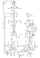
- the figure shows an amplifier circuit according to the present principle based on a block diagram.
- This comprises an input 1 for supplying a useful signal to be amplified, which is designed as a balanced input with an input terminal pair.
- the amplified by the present amplifier circuit signal which is derived from the signal applied to the input 1, can be tapped at the output 2, which is also formed symmetrically as an output terminal pair.
- an amplifier 3 which forms a signal from the difference from the input 1 and provided by the output 2 signal.
- This difference signal is provided at the balanced input of the operational amplifier 3.
- the output terminal pair 2 is connected via a respective resistor 4, 5 to the input of the amplifier 3.
- the two output terminals of the operational amplifier 3 are connected in an inverting feedback via a respective capacitor 6, 7 with the two inputs of the amplifier 3.
- the amplifier 3 has in addition to the differential input and the differential output still a common mode input for supplying a common mode level V CM . At this a common mode signal, a so-called common-mode signal, can be fed.
- CMOS inverter 13 To one of the two output terminals of the differential amplifier 3, the positive input of a comparator 8 is connected, whose negative input is connected to a signal generator 9. The output of the pulse width modulation PWM designed comparator 8 is connected directly to a first output driver 10 and to a second output driver 11 via an inverter 12. The output drivers 10, 11 are each connected to the control inputs of a CMOS inverter 13, 14.
- the CMOS inverters 13, 14 each comprise, as is customary in CMOS inverters, a load-side series circuit of a p-channel and an n-channel MOS transistor, which are connected between a supply potential terminal 15 and a reference potential terminal 16.
- the outputs of the CMOS inverters 13, 14, which form the output stages of the present amplifier, have their output nodes at the connection node of the MOS transistors, respectively. These output nodes are connected via a series inductance 17, 18 with the output terminals 2. Between the output terminals 2, a stabilizing capacitor 19 is connected, which forms an LC filter together with the series inductances 17, 18.
- the signal generator 9 is designed as a triangular signal generator which provides a periodic signal with a peak-to-peak voltage V max -V min at an output 20 resulting from the difference of an upper peak value V max and a lower peak value V min .
- the processed as a digital clock signal frequency of the signal generator provided by the periodic signal is provided at a digital clock output 21 which is connected to a first input of a phase detector 22. Another input of the phase detector 22 is connected to a reference clock source 23.
- the output of the phase detector 22, at which a possible phase deviation of the two input signals is available from each other, is guided via a voltage-current converter 24 to the quiescent current input 25 of the signal generator 9.
- the amplitude V max -V min is set at a symmetrically formed amplitude control input 26 of the signal generator 9.
- the differential output of another operational amplifier 27 is connected.
- the negative input of the operational amplifier 27 is connected via a resistor 28 to the reference potential 16.
- the plus input of the operational amplifier 27 is connected via a further resistor 29 to the supply potential terminal 15.
- Supply and reference potential terminal 15, 16 coincide with the supply voltage terminals 15, 16 of the output stages 13, 14 of the amplifier.
- the operational amplifier 27 also has a common mode input connected to the common mode input of the operational amplifier 3 for supplying the common mode signal V CM .
- the operational amplifier 27 has a negative feedback to the differential input via a respective resistor 30, 31 with respect to the differential output.
- the peak-to-peak voltage V max -V min of the ramp signal provided by the signal generator 9 is proportional to the supply voltage of the amplifier.
- the bias current of the signal generator 9 is controlled by a phase-locked loop to keep the frequency of the periodic signal constant while the peak-to-peak voltage V max -V min changes.
- the bandwidth of both control loops, namely that of the amplifier and that of the phase controller, are greater than the cut-off frequency of the low-pass filter.
- the linearity of the output stage is significantly improved. Another improvement could be, for example, by increasing the bandwidth the open loop gain can be achieved. With the presented feed-forward technique there is no need for error compensation for any noise components on the supply voltage.
- the described principle namely to set the peak-to-peak voltage of the periodic signal in proportion to the supply voltage, allows a significant improvement in the supply voltage suppression and, at the same time, a considerable avoidance of undesirable folding effects.
- the described principle can be implemented with particularly simple circuit technology and with little effort.
- a digital implementation can also be provided.
- the supply voltage would be converted into a digital voltage signal using an analog / digital converter and the duty cycle of the pulse width modulation would be tracked in proportion to the supply voltage.
Abstract
Claims (8)
- Circuit amplificateur comportant- une entrée (1) pour l'entrée d'un signal utile à amplifier,- une sortie (2) pour prélever un signal utile amplifié,- un amplificateur (3) différentiel comportant une première entrée, qui est reliée à l'entrée du circuit amplificateur, une deuxième entrée, qui est couplée à la sortie du circuit amplificateur et une sortie,- un comparateur (8) comportant une première entrée, qui est raccordée à la sortie de l'amplificateur (3) différentiel, et une deuxième entrée, à laquelle est envoyé un signal périodique,- un étage (13) de sortie comportant une entrée, qui est couplée à une sortie du comparateur (8), une sortie et une borne (15) d'alimentation pour appliquer une tension d'alimentation, et- un générateur (9) de signal, qui est raccordé à la deuxième entrée du comparateur (8) et qui met à disposition le signal périodique avec une amplitude qui est proportionnelle à la tension d'alimentation de l'étage de sortie, le générateur (9) de signal étant disposé dans une boucle (9, 22, 24) d'asservissement de phase pour la régulation de la fréquence du signal périodique en fonction d'une cadence de référence.
- Circuit amplificateur suivant la revendication 1, caractérisé en ce qu'il est prévu un amplificateur (27) opérationnel qui comporte deux entrées, qui sont reliées à une borne (15, 16) d'alimentation et à une borne de potentiel de référence pour appliquer la tension d'alimentation de l'étage (13) de sortie et une sortie, qui est reliée à une entrée (26) de commande d'amplitude du générateur (9) de signal.
- Circuit amplificateur suivant la revendication 1 ou 2, caractérisé en ce que la boucle (9, 22, 24) d'asservissement de phase comporte un détecteur (22) de phase, comportant une première entrée de cadencement, qui est reliée à une sortie de cadencement du générateur (9) de signal pour la transmission de la fréquence du signal périodique, une deuxième entrée, qui est reliée à une source (23) de référence pour l'amenée de la cadence de référence et une sortie, qui est couplée à une entrée de courant de repos du générateur (9) de signal.
- Circuit amplificateur suivant l'une des revendications 1 à 3, caractérisé en ce que le générateur (9) de signal est réalisé sous la forme d'un générateur de signal à rampe ou sous la forme d'un générateur de signal en forme de dents de scie.
- Circuit amplificateur suivant l'une des revendications 1 à 4, caractérisé en ce qu'il est prévu un filtre (17, 18, 19) qui comporte une inductance (17) série et qui est raccordé à la sortie de l'étage de sortie (13).
- Circuit amplificateur suivant l'une des revendications 1 à 5, caractérisé en ce le circuit amplificateur comporte une sortie (2) symétrique comportant un étage (14) de sortie supplémentaire qui a une entrée qui est couplée par l'intermédiaire d'un inverseur (12) à la sortie du comparateur (8).
- Circuit amplificateur suivant la revendication 6, caractérisé en ce que l'étage (13) de sortie et l'étage (14) supplémentaire comportent chacun un inverseur CMOS.
- Circuit amplificateur suivant la revendication 6 ou 7, caractérisé en ce que le filtre (17, 18, 19) comporte une inductance (18) série supplémentaire, qui effectue le couplage de l'étage (14) de sortie supplémentaire avec la sortie (2).
Applications Claiming Priority (3)
| Application Number | Priority Date | Filing Date | Title |
|---|---|---|---|
| DE10231183A DE10231183A1 (de) | 2002-07-10 | 2002-07-10 | Verstärkerschaltung |
| DE10231183 | 2002-07-10 | ||
| PCT/DE2003/002304 WO2004008632A1 (fr) | 2002-07-10 | 2003-07-09 | Circuit amplificateur |
Publications (2)
| Publication Number | Publication Date |
|---|---|
| EP1520341A1 EP1520341A1 (fr) | 2005-04-06 |
| EP1520341B1 true EP1520341B1 (fr) | 2006-11-22 |
Family
ID=29796249
Family Applications (1)
| Application Number | Title | Priority Date | Filing Date |
|---|---|---|---|
| EP03763603A Expired - Fee Related EP1520341B1 (fr) | 2002-07-10 | 2003-07-09 | Circuit amplificateur |
Country Status (5)
| Country | Link |
|---|---|
| US (1) | US7068095B2 (fr) |
| EP (1) | EP1520341B1 (fr) |
| CN (1) | CN100472954C (fr) |
| DE (2) | DE10231183A1 (fr) |
| WO (1) | WO2004008632A1 (fr) |
Families Citing this family (33)
| Publication number | Priority date | Publication date | Assignee | Title |
|---|---|---|---|---|
| US7161428B2 (en) * | 2004-04-26 | 2007-01-09 | Rgb Systems, Inc. | Method and apparatus for extending the bandwidth of a Class D amplifier circuit |
| EP1612934B1 (fr) * | 2004-06-29 | 2018-07-25 | Lantiq Beteiligungs-GmbH & Co.KG | Amplificateur de classe D |
| US7348847B2 (en) | 2005-04-28 | 2008-03-25 | Sige Semiconductor Inc. | Integrated implementation of a collector boost scheme and method therefor |
| US7317355B2 (en) * | 2005-05-10 | 2008-01-08 | Texas Instruments Incorporated | Over-current detection for a power field-effect transistor (FET) |
| US7615978B2 (en) * | 2005-07-22 | 2009-11-10 | Fairchild Semiconductor Corporation | Current mode control with feed-forward for power devices |
| US7446603B2 (en) * | 2006-08-17 | 2008-11-04 | Matsushita Electric Industrial Co., Ltd. | Differential input Class D amplifier |
| JP4855886B2 (ja) * | 2006-10-02 | 2012-01-18 | 株式会社東芝 | 電力増幅装置 |
| US7598895B1 (en) * | 2008-04-01 | 2009-10-06 | Silicon Laboratories, Inc. | System and method of altering a PWM carrier power spectrum |
| US7791521B2 (en) * | 2008-04-01 | 2010-09-07 | Silicon Laboratories, Inc. | System and method of changing a PWM power spectrum |
| US7701307B2 (en) * | 2008-04-01 | 2010-04-20 | Silicon Laboratories, Inc. | System and method of changing a PWM power spectrum |
| GB2459304B (en) * | 2008-04-18 | 2013-02-20 | Nujira Ltd | Improved pulse width modulation |
| US20100027813A1 (en) * | 2008-07-31 | 2010-02-04 | Fortemedia, Inc. | Switching audio amplifier, digital speaking device and audio amplification method |
| TWI380580B (en) * | 2009-08-20 | 2012-12-21 | Richtek Technology Corp | Variable frequency class-d amplifier and a control method thereof and a ramp generator for the variable freguency class-d amplifier and a method thereof |
| EP2341616B1 (fr) * | 2009-12-23 | 2013-04-24 | STMicroelectronics Design and Application S.R.O. | Amplificateur de commande de charge capacitive |
| US8130128B2 (en) | 2010-03-30 | 2012-03-06 | Silicon Laboratores Inc. | System and method for generating shaped noise |
| KR101706240B1 (ko) * | 2010-12-30 | 2017-02-27 | 엘지디스플레이 주식회사 | 차동신호수신회로 및 이의 구동방법 |
| CN102938639B (zh) * | 2011-08-15 | 2015-12-16 | 上海普锐马电子有限公司 | 一种大功率放大电路 |
| CN102984630B (zh) * | 2011-09-06 | 2015-12-02 | 昂宝电子(上海)有限公司 | 用于音频放大系统中减少失真的系统和方法 |
| CN102984629B (zh) | 2011-09-06 | 2014-12-17 | 昂宝电子(上海)有限公司 | 用于音频放大系统中降噪的方法 |
| DE102012104488A1 (de) * | 2012-05-24 | 2013-11-28 | Hochschule für angewandte Wissenschaften München | Geschalteter Verstärker für variable Versorgungsspannung |
| US9086708B2 (en) * | 2012-12-31 | 2015-07-21 | Gazelle Semiconductor Inc. | High slew rate switching regulator circuits and methods |
| US9735574B2 (en) | 2012-12-31 | 2017-08-15 | Gazelle Semiconductor, Inc. | Switching regulator circuits and methods |
| US9577532B2 (en) | 2013-07-25 | 2017-02-21 | Gazelle Semiconductor, Inc. | Switching regulator circuits and methods |
| US9685919B2 (en) | 2013-08-21 | 2017-06-20 | On-Bright Electronics (Shanghai) Co., Ltd. | Amplification systems and methods with output regulation |
| CN103441739B (zh) | 2013-08-21 | 2015-04-22 | 昂宝电子(上海)有限公司 | 具有一个或多个通道的放大系统和方法 |
| US9866104B2 (en) | 2013-11-26 | 2018-01-09 | Gazelle Semiconductor, Inc. | Circuits and methods for operating a switching regulator |
| US9444340B2 (en) | 2014-06-26 | 2016-09-13 | Gazelle Semiconductor, Inc. | Circuits and methods for providing current to a load |
| US10444261B2 (en) * | 2014-12-22 | 2019-10-15 | Sony Corporation | Signal detector, electronic device, and method for controlling signal detector |
| CN106961274A (zh) * | 2016-12-14 | 2017-07-18 | 天津天喜国瑞科技发展有限公司 | 信号放大器电路 |
| US10116268B2 (en) * | 2017-01-09 | 2018-10-30 | Analog Devices Global | Operational amplifier |
| CN112398450B (zh) * | 2019-08-13 | 2023-09-01 | 博通集成电路(上海)股份有限公司 | 功率放大器和操作功率放大器的方法 |
| CN113141163B (zh) * | 2020-01-19 | 2023-11-17 | 晶豪科技股份有限公司 | D类功率放大器电路 |
| US11251760B2 (en) | 2020-05-20 | 2022-02-15 | Analog Devices, Inc. | Amplifiers with wide input range and low input capacitance |
Family Cites Families (7)
| Publication number | Priority date | Publication date | Assignee | Title |
|---|---|---|---|---|
| US5590033A (en) * | 1988-09-02 | 1996-12-31 | Yamaha Corporation | Power source apparatus |
| JPH04281606A (ja) * | 1991-03-11 | 1992-10-07 | Matsushita Electric Ind Co Ltd | パルス幅変調増幅器 |
| US5559467A (en) * | 1995-01-27 | 1996-09-24 | The Regents Of The University Of California | Digital, pulse width modulation audio power amplifier with noise and ripple shaping |
| US6016075A (en) * | 1997-06-04 | 2000-01-18 | Lord Corporation | Class-D amplifier input structure |
| AU3933700A (en) * | 1999-03-16 | 2000-10-04 | Audiologic, Incorporated | Power supply compensation for noise shaped, digital amplifiers |
| US20020060605A1 (en) * | 2000-09-22 | 2002-05-23 | Kowkutla Venkateswar R. | Amplifiers |
| JP3941443B2 (ja) * | 2001-09-27 | 2007-07-04 | ヤマハ株式会社 | 自走式pwm増幅器 |
-
2002
- 2002-07-10 DE DE10231183A patent/DE10231183A1/de not_active Ceased
-
2003
- 2003-07-09 EP EP03763603A patent/EP1520341B1/fr not_active Expired - Fee Related
- 2003-07-09 WO PCT/DE2003/002304 patent/WO2004008632A1/fr active IP Right Grant
- 2003-07-09 CN CNB038162474A patent/CN100472954C/zh not_active Expired - Fee Related
- 2003-07-09 DE DE50305767T patent/DE50305767D1/de not_active Expired - Lifetime
-
2005
- 2005-01-10 US US11/032,703 patent/US7068095B2/en not_active Expired - Fee Related
Also Published As
| Publication number | Publication date |
|---|---|
| WO2004008632A1 (fr) | 2004-01-22 |
| CN100472954C (zh) | 2009-03-25 |
| DE50305767D1 (de) | 2007-01-04 |
| DE10231183A1 (de) | 2004-01-29 |
| EP1520341A1 (fr) | 2005-04-06 |
| US7068095B2 (en) | 2006-06-27 |
| CN1666411A (zh) | 2005-09-07 |
| US20050200404A1 (en) | 2005-09-15 |
Similar Documents
| Publication | Publication Date | Title |
|---|---|---|
| EP1520341B1 (fr) | Circuit amplificateur | |
| DE69735029T2 (de) | Selbst-oszillierender Klasse-D Verstärker mit verbesserter Kaskaden-Rückkopplung | |
| DE60311681T2 (de) | Leistungsverstärkungsvorrichtung | |
| DE102005028747B4 (de) | Mischeranordnung, Verwendung der Mischeranordnung und Verfahren zur Frequenzumsetzung | |
| US8981832B2 (en) | Amplification systems and methods with distortion reductions | |
| DE602004004230T2 (de) | Klasse-D Verstärker | |
| DE19837153A1 (de) | Pulsweitenmodulierter Gleichspannungswandler | |
| DE102018114919A1 (de) | Abwärtsspannungswandler und -verfahren | |
| DE3131763C2 (de) | AM-Detektorschaltung | |
| DE102019206995A1 (de) | Aktives filter mit adaptiver verstärkung für hochfrequenz-dc-dc-wandlerohne teiler | |
| DE102021124257A1 (de) | Schaltung zum Steuern eines Leistungswandlers, System mit Leistungswandler und Verfahren | |
| EP1310043B1 (fr) | Amplificateur differentiel complementaire | |
| DE10233243B4 (de) | Schaltungsanordnung zur Regeneration von Taktsignalen | |
| EP0174538A1 (fr) | Alimentation à découpage avec un premier étage régulateur et un étage auxiliaire en parallèle | |
| EP1388200B1 (fr) | Montage de stabilisation de tension | |
| DE112022002683T5 (de) | Treiberschaltung und betrieb | |
| EP1389359A2 (fr) | Convertisseur continu-continu dote d'un regulateur de commutation | |
| DE102008025347B4 (de) | Elektronischer Verstärker | |
| WO2014154548A1 (fr) | Agencement de circuit et procédé d'excitation d'un transformateur piézoélectrique | |
| DE3026551C2 (fr) | ||
| DE4007953C2 (de) | Gleichspannungswandler mit geschalteten Kondensatoren | |
| DE2557512C3 (de) | PDM-Verstärker | |
| DE602004008857T2 (de) | Leistungsverstärkungsschaltung | |
| DE102004060212A1 (de) | Pegelumsetzer | |
| DE2648080B2 (de) | Breitbandverstärker mit veränderbarer Verstärkung |
Legal Events
| Date | Code | Title | Description |
|---|---|---|---|
| PUAI | Public reference made under article 153(3) epc to a published international application that has entered the european phase |
Free format text: ORIGINAL CODE: 0009012 |
|
| 17P | Request for examination filed |
Effective date: 20050119 |
|
| AK | Designated contracting states |
Kind code of ref document: A1 Designated state(s): AT BE BG CH CY CZ DE DK EE ES FI FR GB GR HU IE IT LI LU MC NL PT RO SE SI SK TR |
|
| RBV | Designated contracting states (corrected) |
Designated state(s): DE |
|
| GRAP | Despatch of communication of intention to grant a patent |
Free format text: ORIGINAL CODE: EPIDOSNIGR1 |
|
| GRAS | Grant fee paid |
Free format text: ORIGINAL CODE: EPIDOSNIGR3 |
|
| GRAA | (expected) grant |
Free format text: ORIGINAL CODE: 0009210 |
|
| AK | Designated contracting states |
Kind code of ref document: B1 Designated state(s): DE |
|
| REF | Corresponds to: |
Ref document number: 50305767 Country of ref document: DE Date of ref document: 20070104 Kind code of ref document: P |
|
| PLBE | No opposition filed within time limit |
Free format text: ORIGINAL CODE: 0009261 |
|
| STAA | Information on the status of an ep patent application or granted ep patent |
Free format text: STATUS: NO OPPOSITION FILED WITHIN TIME LIMIT |
|
| 26N | No opposition filed |
Effective date: 20070823 |
|
| REG | Reference to a national code |
Ref country code: DE Ref legal event code: R081 Ref document number: 50305767 Country of ref document: DE Owner name: INTEL MOBILE COMMUNICATIONS GMBH, DE Free format text: FORMER OWNER: INFINEON TECHNOLOGIES AG, 81669 MUENCHEN, DE Effective date: 20130314 Ref country code: DE Ref legal event code: R081 Ref document number: 50305767 Country of ref document: DE Owner name: INTEL MOBILE COMMUNICATIONS GMBH, DE Free format text: FORMER OWNER: INTEL MOBILE COMMUNICATIONS TECHNOLOGY GMBH, 85579 NEUBIBERG, DE Effective date: 20130326 Ref country code: DE Ref legal event code: R081 Ref document number: 50305767 Country of ref document: DE Owner name: INTEL MOBILE COMMUNICATIONS GMBH, DE Free format text: FORMER OWNER: INTEL MOBILE COMMUNICATIONS GMBH, 85579 NEUBIBERG, DE Effective date: 20130315 Ref country code: DE Ref legal event code: R081 Ref document number: 50305767 Country of ref document: DE Owner name: INTEL MOBILE COMMUNICATIONS GMBH, DE Free format text: FORMER OWNER: INFINEON TECHNOLOGIES AG, 85579 NEUBIBERG, DE Effective date: 20130315 Ref country code: DE Ref legal event code: R081 Ref document number: 50305767 Country of ref document: DE Owner name: INTEL DEUTSCHLAND GMBH, DE Free format text: FORMER OWNER: INTEL MOBILE COMMUNICATIONS GMBH, 85579 NEUBIBERG, DE Effective date: 20130315 Ref country code: DE Ref legal event code: R081 Ref document number: 50305767 Country of ref document: DE Owner name: INTEL DEUTSCHLAND GMBH, DE Free format text: FORMER OWNER: INTEL MOBILE COMMUNICATIONS TECHNOLOGY GMBH, 85579 NEUBIBERG, DE Effective date: 20130326 Ref country code: DE Ref legal event code: R081 Ref document number: 50305767 Country of ref document: DE Owner name: INTEL DEUTSCHLAND GMBH, DE Free format text: FORMER OWNER: INFINEON TECHNOLOGIES AG, 85579 NEUBIBERG, DE Effective date: 20130315 Ref country code: DE Ref legal event code: R081 Ref document number: 50305767 Country of ref document: DE Owner name: INTEL DEUTSCHLAND GMBH, DE Free format text: FORMER OWNER: INFINEON TECHNOLOGIES AG, 81669 MUENCHEN, DE Effective date: 20130314 |
|
| REG | Reference to a national code |
Ref country code: DE Ref legal event code: R081 Ref document number: 50305767 Country of ref document: DE Owner name: INTEL DEUTSCHLAND GMBH, DE Free format text: FORMER OWNER: INTEL MOBILE COMMUNICATIONS GMBH, 85579 NEUBIBERG, DE |
|
| REG | Reference to a national code |
Ref country code: DE Ref legal event code: R081 Ref document number: 50305767 Country of ref document: DE Owner name: APPLE INC., CUPERTINO, US Free format text: FORMER OWNER: INTEL DEUTSCHLAND GMBH, 85579 NEUBIBERG, DE |
|
| PGFP | Annual fee paid to national office [announced via postgrant information from national office to epo] |
Ref country code: DE Payment date: 20200624 Year of fee payment: 18 |
|
| REG | Reference to a national code |
Ref country code: DE Ref legal event code: R119 Ref document number: 50305767 Country of ref document: DE |
|
| PG25 | Lapsed in a contracting state [announced via postgrant information from national office to epo] |
Ref country code: DE Free format text: LAPSE BECAUSE OF NON-PAYMENT OF DUE FEES Effective date: 20220201 |