EP1518271B1 - Verfahren und Anordnung von Nanoröhrchen zum Kühlen und Erden von Chips - Google Patents
Verfahren und Anordnung von Nanoröhrchen zum Kühlen und Erden von Chips Download PDFInfo
- Publication number
- EP1518271B1 EP1518271B1 EP03763132.2A EP03763132A EP1518271B1 EP 1518271 B1 EP1518271 B1 EP 1518271B1 EP 03763132 A EP03763132 A EP 03763132A EP 1518271 B1 EP1518271 B1 EP 1518271B1
- Authority
- EP
- European Patent Office
- Prior art keywords
- nanotubes
- die
- thermal management
- management aid
- array
- Prior art date
- Legal status (The legal status is an assumption and is not a legal conclusion. Google has not performed a legal analysis and makes no representation as to the accuracy of the status listed.)
- Expired - Lifetime
Links
Images


Classifications
-
- H—ELECTRICITY
- H10—SEMICONDUCTOR DEVICES; ELECTRIC SOLID-STATE DEVICES NOT OTHERWISE PROVIDED FOR
- H10W—GENERIC PACKAGES, INTERCONNECTIONS, CONNECTORS OR OTHER CONSTRUCTIONAL DETAILS OF DEVICES COVERED BY CLASS H10
- H10W40/00—Arrangements for thermal protection or thermal control
- H10W40/70—Fillings or auxiliary members in containers or in encapsulations for thermal protection or control
- H10W40/77—Auxiliary members characterised by their shape
-
- B—PERFORMING OPERATIONS; TRANSPORTING
- B82—NANOTECHNOLOGY
- B82Y—SPECIFIC USES OR APPLICATIONS OF NANOSTRUCTURES; MEASUREMENT OR ANALYSIS OF NANOSTRUCTURES; MANUFACTURE OR TREATMENT OF NANOSTRUCTURES
- B82Y10/00—Nanotechnology for information processing, storage or transmission, e.g. quantum computing or single electron logic
-
- H—ELECTRICITY
- H10—SEMICONDUCTOR DEVICES; ELECTRIC SOLID-STATE DEVICES NOT OTHERWISE PROVIDED FOR
- H10W—GENERIC PACKAGES, INTERCONNECTIONS, CONNECTORS OR OTHER CONSTRUCTIONAL DETAILS OF DEVICES COVERED BY CLASS H10
- H10W40/00—Arrangements for thermal protection or thermal control
- H10W40/20—Arrangements for cooling
- H10W40/25—Arrangements for cooling characterised by their materials
-
- B—PERFORMING OPERATIONS; TRANSPORTING
- B82—NANOTECHNOLOGY
- B82Y—SPECIFIC USES OR APPLICATIONS OF NANOSTRUCTURES; MEASUREMENT OR ANALYSIS OF NANOSTRUCTURES; MANUFACTURE OR TREATMENT OF NANOSTRUCTURES
- B82Y30/00—Nanotechnology for materials or surface science, e.g. nanocomposites
-
- Y—GENERAL TAGGING OF NEW TECHNOLOGICAL DEVELOPMENTS; GENERAL TAGGING OF CROSS-SECTIONAL TECHNOLOGIES SPANNING OVER SEVERAL SECTIONS OF THE IPC; TECHNICAL SUBJECTS COVERED BY FORMER USPC CROSS-REFERENCE ART COLLECTIONS [XRACs] AND DIGESTS
- Y10—TECHNICAL SUBJECTS COVERED BY FORMER USPC
- Y10S—TECHNICAL SUBJECTS COVERED BY FORMER USPC CROSS-REFERENCE ART COLLECTIONS [XRACs] AND DIGESTS
- Y10S977/00—Nanotechnology
- Y10S977/70—Nanostructure
- Y10S977/832—Nanostructure having specified property, e.g. lattice-constant, thermal expansion coefficient
- Y10S977/833—Thermal property of nanomaterial, e.g. thermally conducting/insulating or exhibiting peltier or seebeck effect
Definitions
- the present invention pertains generally to thermal management of an integrated circuit package containing at least one die, and in particular to methods and apparatus for providing thermal and electrical connection between a die and a thermal management aid using an array of carbon nanotubes.
- US 6,407,922 B1 discloses a heat spreader including a matrix material, which has incorporated carbon nanotubes and/or thermal pyrolytic graphite flakes.
- the carbon nanotubes and/or thermal pyrolytic graphite flakes are situated between a first surface and a second surface of the heat spreader, to transfer heat from a heat source adjacent the first surface to a heat sink adjacent the second surface.
- the first surface has a smaller surface area than that of the second surface.
- the carbon nanotubes and/or thermal pyrolytic graphite flakes are aligned extending between the first and second surfaces, and spread out in a direction from the first surface to the second surface to provide more effective heat transfer and uniform spreading of the heat.
- EP 1 199 328 A1 discloses a thermal conductive polymer sheet including a polymer matrix and graphitized carbon fibers as a thermally conductive filler.
- Figure 1 is a simplified schematic elevation view of an embodiment of a package 10 for mounting and cooling a heat generating component 12 that is supported by a mounting structure 20.
- component 12 may also comprise at least one active element such as a component, a module or an active circuit formed on a front surface 14 of component 12 which may be a semiconductor die 12.
- active element such as a component, a module or an active circuit formed on a front surface 14 of component 12 which may be a semiconductor die 12.
- die 12 has a front surface 14 thereof affixed to socket 20 by a ball grid assembly comprised of a plurality of solder balls 22 which are bonded to surface 14 of die 12.
- the other, or backside, surface 16 of die 12 is shown connected to a thermal management aid, such as an integrated heat spreader 24 as shown in the embodiment of Fig. 1 .
- Other thermal management aids may include heat sinks or other similar structures.
- Typical thermal management aids are formed from relatively soft conductive materials such as copper or copper alloys.
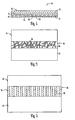
- FIG. 2 is an enlarged detail elevation view of an interface layer 26 between the backside surface 16 of die 12 and the thermal management aid such as an integral heat spreader 24.
- a thermal interface layer 26 having very high heat conductivity in one embodiment, is interposed between elements 12 and 24.
- thermal interface layer 26 is comprised of an array of carbon nanotubes 28 which are mixed with a paste and applied between backside 16 of die 12 and thermal management aid 24.
- a distribution of nanotube lengths is selected to allow substantial percentage of nanotubes 28 to bridge the gap between the die 12 and the heat spreader 24 and form a direct path to provide for optimal thermal coupling between die 12 and heat spreader 24.
- Figure 2 illustrates, in greatly enlarged and expanded form, the relationship between the lengths of nanotubes 28 and the thickness of interface layer 26.
- the nanotubes typically have a diameter on the order of 1 nanometer.
- the thickness of interface layer 26 is from tens to hundreds of nanometers thick, depending upon the nanotube lengths available.
- the lengths of the nanotubes in one embodiment slightly exceed the thickness of interface layer 26 and the thickness of the thermal interface layer is less than about 0.01 to 0.10 mm.
- Figure 3 illustrates another embodiment of the interface layer 26 that also has an array of carbon nanotubes that, in this embodiment, are arranged in a plurality of individual bundles of nanotubes 38.
- the nanotubes 38 are grown directly on the backside surface 16 of die 12 using a chemical vapor deposition (CVD) process.
- the process is set up and controlled to produce bundles of nanotubes 38 which each have their longitudinal axis perpendicular to the surface of die 12.
- This orientation is optimal as the heat condition is optimal along the axis of nanotubes 38 and can be as high as 6000W/mK as compared to a value of about 400 for copper.
- the lengths of the bundles of nanotubes 38 are in the order of several micrometers.
- an interstitial material 40 can be applied to the bundles of nanotubes 38 after they have been grown.
- a number of thermal pastes or polymers can serve as suitable interstitial material 40.
- the thermal conductance from the active elements on the front of the die to the thermal management aid is further reduced by mechanically grinding of the backside surface or otherwise providing for a thinning of the die from the surface not containing the active elements.
- the CVD process of growing bundles of nanotubes on die 12 should, according to an embodiment of the invention, be carried out prior to the fabrication of active circuits on die 12 in order to avoid exposing the active elements to the high temperatures of the CVD process.
- the high tensile strength of the nanotubes allows their tips to be embedded in the surface of the soft thermal management aid such as a heat sink of the integral heat spreader if they are allowed to project from the surface of the interstitial material.
- the material for the thermal management aid is copper or an alloy of copper having a high copper content. This allows the thermal interface layer to compensate for surface roughness of the thermal management aid or the die. Additionally, the projection of the nanotubes beyond the surface of the interstitial material allows the tips of the nanotubes to impinge upon the surface of the thermal management aid in the "valleys" in the surface which are a consequence of the surface roughness.
- the tips of the nanotubes can impinge into the copper surface itself.
- the nanotubes impinge into the surface of the thermal management aid through a layer of solder coating the surface.
- the solder may be softer than the surface of the thermal management aid.
- the surface of the thermal management aid may have a nickel or nickel alloy layer upon which there is a tinned solder layer to receive the projecting tips of the nanotubes.
- the integrated heat spreader is heated so that a portion of it is molten at the time that the time that the surface is connected to the nanotubes projecting from the interstitial layer.
- the mechanical stress on the nanotubes inserted into the soft surface of the thermal management aid is reduced.
- interface layer 26 can also be used to provide a ground connection between die 12 and component socket 20. Providing such a connection supplements grounding connections through solder ball connections to a mounting socket and allows for reducing the package size because not as much of the real estate needs to be committed to providing multiple conventional ground connections.
- Figure 5 illustrates schematically the provision of a ground connection through interface layer 24.
- active elements circuits are on the front side 54 of die 12.
- a plurality of vias 56 are provided through die 12 from the active elements on the front side to the backside 57 of die 12 which, in this embodiment, is metallized over at least a portion of its surface to improve the grounding path from active elements on the front side of die 12 to the die backside.
- Figure 6 shows a socket for supporting the die and providing electrical paths from a die to the socket.
- further contacts 58 are provided on socket 20 for engaging at least one side of the integral heat spreader 24 and conduct electrical current to connectors 60 to be connected to further circuitry external to socket 20 through conductive paths 62.
- connectors are connected to a source of reference potential such as ground.
- Figure 7 is a flow chart of an embodiment of a process to couple a die to a thermal management aid.
- An array of nanotubes is formed 72 on a surface of the die and a thermal management aid is mounted 79 in contact with the array of nanotubes.
- the array of nanotubes is encapsulated 74 along substantially the entire length of a substantial portion of the nanotubes with only the tips of the nanotubes projecting from a surface of the interstitial material to facilitate embedding the tips into the surface and into the surface roughness of the of the thermal management solution to form an interface layer.
- electrical connections may be provided from one or more active elements on the die to a surface of the die 76 and electrically connecting the die through the thermal management aid to a source of reference potential 78.
- Figure 8 is a flow chart of a process to provide a thermal conductive path from a die to a thermal management aid.
- the process comprises forming an array 82 of nanotubes on a surface of the die and mounting the thermal management aid 84 in contact with the array of nanotubes to couple the array of nanotubes to the thermal management aid.
- the process also comprises encapsulating the layer of nanotubes 86 with interstitial material along substantially the entire length of a substantial portion of the nanotubes with only the tips of the nanotubes projecting from a surface of the interstitial material to facilitate embedding the tips into the surface and into the surface roughness of the of the thermal management solution.
Landscapes
- Engineering & Computer Science (AREA)
- Chemical & Material Sciences (AREA)
- Nanotechnology (AREA)
- Physics & Mathematics (AREA)
- Mathematical Physics (AREA)
- Theoretical Computer Science (AREA)
- Crystallography & Structural Chemistry (AREA)
- Cooling Or The Like Of Semiconductors Or Solid State Devices (AREA)
- Carbon And Carbon Compounds (AREA)
Claims (26)
- Gehäuse für integrierte Schaltung, das Folgendes umfasst:einen Chip (12);eine Hilfe (24) für thermisches Management, die über dem Chip montiert ist; undeine Grenzflächenschicht (26), die den Chip und die Hilfe für thermisches Management thermisch koppelt, dadurch gekennzeichnet, dass die Grenzflächenschicht ferner eine Anordnung von Kohlenstoff-Nanoröhren (28) enthält, die in mehreren einzelnen Bündeln angeordnet sind, deren Längsachsen auf eine Rückseite des Chips im Wesentlichen senkrecht ausgerichtet sind.
- Gehäuse nach Anspruch 1, wobei die Anordnung von Kohlenstoff-Nanoröhren in einen Grundstoff aus Einlagerungsmaterial (40) eingekapselt ist.
- Gehäuse nach Anspruch 2, wobei die Dicke der Grenzflächenschicht (26) kleiner als etwa 0,01 mm bis 0,10 mm ist.
- Gehäuse nach Anspruch 2, wobei die Länge eines wesentlichen Abschnitts der Nanoröhren die Dicke des Einlagerungsmaterials (40) geringfügig überschreitet, um einem wesentlichen Abschnitt der Nanoröhren zu ermöglichen, zwischen dem Chip und der Hilfe (24) für thermisches Management eingekeilt zu werden, um Wärme von dem Chip (12) hauptsächlich durch die Nanoröhren (28) eher als durch das umgebende Einlagerungsmaterial (40) zu leiten.
- Gehäuse nach Anspruch 2, wobei die Hilfe (24) für thermisches Management aus einem Metall gebildet ist, das eine Weichheit hat, die wesentlich niedriger ist als die Härte der Nanoröhren (28), und wobei das Einlagerungsmaterial (40) einen wesentlichen Abschnitt der Länge wenigstens eines Abschnitts der Anordnung von Nanoröhren mit Ausnahme der äußersten Enden wenigstens einiger der Nanoröhren, die konstruiert und angeordnet sind, um sich von der Oberfläche des Einlagerungsmaterials zu erstrecken, und die einen Durchmesser besitzen, um die Einbettung der Enden der Nanoröhren in der Oberfläche der Hilfe für thermisches Management zu erleichtern, einkapselt.
- Gehäuse nach Anspruch 2, wobei die Grenzflächenschicht (26) elektrisch leitend ist, um eine Oberfläche des Chips (12) mit einer Referenzpotentialquelle zu koppeln, die durch die Hilfe für thermisches Management getragen wird.
- Gehäuse nach Anspruch 6, wobei die Referenzpotentialquelle ein Anschluss ist, der mit elektrischer Masse verbunden ist.
- Gehäuse nach Anspruch 7, wobei die Oberfläche des Chips (12) mit wenigstens einem Masseanschluss für wenigstens ein aktives Element in dem Chip gekoppelt ist.
- Gehäuse nach Anspruch 2, wobei das Einlagerungsmaterial (40) eine wärmeleitende Paste ist.
- Gehäuse nach Anspruch 2, wobei die Hilfe (24) für thermisches Management ein Kühlkörper ist.
- Gehäuse nach Anspruch 2, wobei die Hilfe (24) für thermisches Management ein einteiliger Wärmeverteiler ist.
- Thermische Grenzflächenschicht für die Verwendung als Zwischenstufe bei der Fertigung eines Schaltungsgehäuses, das einen Chip und eine Hilfe für thermisches Management enthält, wobei die Schicht gekennzeichnet ist durch:eine Anordnung von Kohlenstoff-Nanoröhren (28), die so orientiert sind, dass die Längsachsen eines wesentlichen Anteils der Nanoröhren eine Orientierung haben, die zu der ersten und der zweiten Oberfläche hiervon im Wesentlichen senkrecht ist; undeinen Grundstoff aus Einlagerungsmaterial (40), der die Nanoröhren mit Ausnahme der Spitzen der Nanoröhren, die von der ersten und/oder der zweiten Oberfläche hiervon vorstehen, um in die Hilfe für thermisches Management und/oder in den Chip eingebettet zu werden, im Wesentlichen einkapselt.
- Thermische Grenzflächenschicht nach Anspruch 12, wobei ein wesentlicher Anteil der Nanoröhren (28) der Anordnung von Kohlenstoff-Nanoröhren eine im Wesentlichen gemeinsame Orientierung hat, wobei ihre Längsachsen einen direkten thermischen Pfad von einer ersten zu einer zweiten Oberfläche bilden.
- Thermische Grenzflächenschicht nach Anspruch 12, wobei die Anordnung von Kohlenstoff-Nanoröhren (28) ein Bündel ähnlich ausgerichteter Kohlenstoff-Nanoröhren umfasst, die von der Oberfläche des Chips vorstehen.
- Thermische Grenzflächenschicht nach Anspruch 12, wobei die Anordnung von Nanoröhren mehrere einzelne Kohlenstoff-Nanoröhren umfasst.
- Verfahren zum Koppeln eines Chips mit einer Hilfe für thermisches Management, das Folgendes umfasst:Bilden (72) einer Anordnung von Nanoröhren auf einer Oberfläche des Chips, wobei die Anordnung von Nanoröhren im Wesentlichen senkrecht zu dem Chip und zu der Hilfe für thermisches Management orientiert ist; undMontieren (79) der Hilfe für thermisches Management in der Nähe und in Kontakt zu der Anordnung von Nanoröhren, um den Chip mit der Hilfe für thermisches Management zu koppeln.
- Verfahren nach Anspruch 16, das außerdem das Einkapseln (74) der Schicht von Nanoröhren mit Einlagerungsmaterial im Wesentlichen auf der gesamten Länge eines wesentlichen Abschnitts der Nanoröhren umfasst, wobei nur die Spitzen der Nanoröhren von einer Oberfläche des Einlagerungsmaterials vorstehen, um das Einbetten der Spitzen in die Oberfläche und in die Oberflächenrauheit der Hilfe für thermisches Management zu erleichtern.
- Verfahren nach Anspruch 16, wobei das Bilden der Anordnung von Nanoröhren das Bewirken, das Bündel von Nanoröhren auf der Oberfläche des Chips wachsen, umfasst.
- Verfahren nach Anspruch 16, das außerdem das Bereitstellen (76) von elektrischen Verbindungen von wenigstens einer aktiven Schaltung auf dem Chip mit der Oberfläche des Chips und das Verwenden der Grenzflächenschicht, um den Chip über die Hilfe für thermisches Management mit einer Referenzpotentialquelle elektrisch zu verbinden, umfasst.
- Verfahren nach Anspruch 16, wobei das Bilden (72) der Anordnung von Nanoröhren das Mischen mehrerer Kohlenstoff-Nanoröhren in eine Paste und das Aufbringen der Paste zwischen die Oberfläche des Chips und die Hilfe für thermisches Management umfasst.
- Verfahren nach Anspruch 16, wobei der Chip gefräst wird, um die Oberfläche näher an wenigstens eine aktive Schaltung in dem Chip zu bewegen.
- Verfahren nach Anspruch 16, wobei das Bilden der Schicht von Nanoröhren auf der hinteren Oberfläche des Chips der Fertigung aktiver Vorrichtungen auf der vorderen Oberfläche des Chips vorhergeht.
- Verfahren zum Bereitstellen eines Wärmeleitungspfades von einem Schaltungschip zu einer Hilfe für thermisches Management, wobei das Verfahren Folgendes umfasst:Positionieren der Hilfe für thermisches Management in der Nähe des Chips; undBilden (72) einer Anordnung von Nanoröhren zwischen der Oberfläche des Chips und der Hilfe für thermisches Management, wobei die Schicht von Nanoröhren einen Wärmeleitungspfad zwischen dem Chip und der Hilfe für thermisches Management bildet, dadurch gekennzeichnet, dass die Anordnung von Nanoröhren zu dem Chip und der Hilfe für thermisches Management im Wesentlichen senkrecht ist.
- Verfahren nach Anspruch 23, wobei das Bilden der Anordnung von Nanoröhren das Mischen mehrerer Nanoröhren in eine Paste und das Aufbringen des Gemischs auf eine Oberfläche des Chips umfasst.
- Verfahren nach Anspruch 23, wobei das Bilden der Anordnung von Nanoröhren das Bilden mehrerer Bündel von Nanoröhren auf der Oberfläche des Chips umfasst.
- Verfahren nach Anspruch 25 wobei das Verfahren des Bildens der mehreren Bündel von Nanoröhren einen Prozess des chemischen Abscheidens aus der Dampfphase umfasst.
Priority Applications (1)
| Application Number | Priority Date | Filing Date | Title |
|---|---|---|---|
| EP15181471.2A EP2962985A1 (de) | 2002-07-02 | 2003-07-02 | Verfahren und vorrichtung mit verwendung von nanoröhrchen zur kühlung und erdung von chips |
Applications Claiming Priority (3)
| Application Number | Priority Date | Filing Date | Title |
|---|---|---|---|
| US10/187,513 US6856016B2 (en) | 2002-07-02 | 2002-07-02 | Method and apparatus using nanotubes for cooling and grounding die |
| US187513 | 2002-07-02 | ||
| PCT/US2003/020889 WO2004006330A1 (en) | 2002-07-02 | 2003-07-02 | Method and apparatus using nanotubes for cooling and grounding die |
Related Child Applications (1)
| Application Number | Title | Priority Date | Filing Date |
|---|---|---|---|
| EP15181471.2A Division EP2962985A1 (de) | 2002-07-02 | 2003-07-02 | Verfahren und vorrichtung mit verwendung von nanoröhrchen zur kühlung und erdung von chips |
Publications (2)
| Publication Number | Publication Date |
|---|---|
| EP1518271A1 EP1518271A1 (de) | 2005-03-30 |
| EP1518271B1 true EP1518271B1 (de) | 2015-08-19 |
Family
ID=29999370
Family Applications (2)
| Application Number | Title | Priority Date | Filing Date |
|---|---|---|---|
| EP15181471.2A Withdrawn EP2962985A1 (de) | 2002-07-02 | 2003-07-02 | Verfahren und vorrichtung mit verwendung von nanoröhrchen zur kühlung und erdung von chips |
| EP03763132.2A Expired - Lifetime EP1518271B1 (de) | 2002-07-02 | 2003-07-02 | Verfahren und Anordnung von Nanoröhrchen zum Kühlen und Erden von Chips |
Family Applications Before (1)
| Application Number | Title | Priority Date | Filing Date |
|---|---|---|---|
| EP15181471.2A Withdrawn EP2962985A1 (de) | 2002-07-02 | 2003-07-02 | Verfahren und vorrichtung mit verwendung von nanoröhrchen zur kühlung und erdung von chips |
Country Status (8)
| Country | Link |
|---|---|
| US (1) | US6856016B2 (de) |
| EP (2) | EP2962985A1 (de) |
| KR (1) | KR100681368B1 (de) |
| CN (1) | CN1666335B (de) |
| AU (1) | AU2003261105A1 (de) |
| MY (1) | MY134315A (de) |
| TW (1) | TWI301659B (de) |
| WO (1) | WO2004006330A1 (de) |
Families Citing this family (84)
| Publication number | Priority date | Publication date | Assignee | Title |
|---|---|---|---|---|
| US6921462B2 (en) | 2001-12-17 | 2005-07-26 | Intel Corporation | Method and apparatus for producing aligned carbon nanotube thermal interface structure |
| US6994584B1 (en) * | 2002-08-30 | 2006-02-07 | Advanced Micro Devices, Inc. | Thermally conductive integrated circuit mounting structures |
| US6867978B2 (en) * | 2002-10-08 | 2005-03-15 | Intel Corporation | Integrated heat spreader package for heat transfer and for bond line thickness control and process of making |
| CN1296994C (zh) * | 2002-11-14 | 2007-01-24 | 清华大学 | 一种热界面材料及其制造方法 |
| AU2003294588A1 (en) * | 2002-12-09 | 2004-06-30 | Rensselaer Polytechnic Institute | Embedded nanotube array sensor and method of making a nanotube polymer composite |
| TWI250203B (en) * | 2002-12-31 | 2006-03-01 | Hon Hai Prec Ind Co Ltd | Thermal interface material |
| US7656027B2 (en) * | 2003-01-24 | 2010-02-02 | Nanoconduction, Inc. | In-chip structures and methods for removing heat from integrated circuits |
| US20040152240A1 (en) * | 2003-01-24 | 2004-08-05 | Carlos Dangelo | Method and apparatus for the use of self-assembled nanowires for the removal of heat from integrated circuits |
| US7316061B2 (en) * | 2003-02-03 | 2008-01-08 | Intel Corporation | Packaging of integrated circuits with carbon nano-tube arrays to enhance heat dissipation through a thermal interface |
| US7094679B1 (en) | 2003-03-11 | 2006-08-22 | The United States Of America As Represented By The Administrator Of The National Aeronautics And Space Administration | Carbon nanotube interconnect |
| US7273095B2 (en) | 2003-03-11 | 2007-09-25 | United States Of America As Represented By The Administrator Of The National Aeronautics And Space Administration | Nanoengineered thermal materials based on carbon nanotube array composites |
| US7112472B2 (en) * | 2003-06-25 | 2006-09-26 | Intel Corporation | Methods of fabricating a composite carbon nanotube thermal interface device |
| US7168484B2 (en) * | 2003-06-30 | 2007-01-30 | Intel Corporation | Thermal interface apparatus, systems, and methods |
| US8048688B2 (en) * | 2006-10-24 | 2011-11-01 | Samsung Electronics Co., Ltd. | Method and apparatus for evaluation and improvement of mechanical and thermal properties of CNT/CNF arrays |
| US7732918B2 (en) * | 2003-08-25 | 2010-06-08 | Nanoconduction, Inc. | Vapor chamber heat sink having a carbon nanotube fluid interface |
| US20070126116A1 (en) * | 2004-08-24 | 2007-06-07 | Carlos Dangelo | Integrated Circuit Micro-Cooler Having Tubes of a CNT Array in Essentially the Same Height over a Surface |
| US7538422B2 (en) * | 2003-08-25 | 2009-05-26 | Nanoconduction Inc. | Integrated circuit micro-cooler having multi-layers of tubes of a CNT array |
| US20070114658A1 (en) * | 2004-08-24 | 2007-05-24 | Carlos Dangelo | Integrated Circuit Micro-Cooler with Double-Sided Tubes of a CNT Array |
| US7109581B2 (en) | 2003-08-25 | 2006-09-19 | Nanoconduction, Inc. | System and method using self-assembled nano structures in the design and fabrication of an integrated circuit micro-cooler |
| US7477527B2 (en) * | 2005-03-21 | 2009-01-13 | Nanoconduction, Inc. | Apparatus for attaching a cooling structure to an integrated circuit |
| US20050116336A1 (en) * | 2003-09-16 | 2005-06-02 | Koila, Inc. | Nano-composite materials for thermal management applications |
| US20050126766A1 (en) * | 2003-09-16 | 2005-06-16 | Koila,Inc. | Nanostructure augmentation of surfaces for enhanced thermal transfer with improved contact |
| US20050214197A1 (en) * | 2003-09-17 | 2005-09-29 | Molecular Nanosystems, Inc. | Methods for producing and using catalytic substrates for carbon nanotube growth |
| WO2005025734A2 (en) * | 2003-09-17 | 2005-03-24 | Molecular Nanosystems, Inc. | Methods for producing and using catalytic substrates for carbon nanotube growth |
| TW200517042A (en) * | 2003-11-04 | 2005-05-16 | Hon Hai Prec Ind Co Ltd | Heat sink |
| US7456052B2 (en) * | 2003-12-30 | 2008-11-25 | Intel Corporation | Thermal intermediate apparatus, systems, and methods |
| US7180174B2 (en) * | 2003-12-30 | 2007-02-20 | Intel Corporation | Nanotube modified solder thermal intermediate structure, systems, and methods |
| US7612370B2 (en) * | 2003-12-31 | 2009-11-03 | Intel Corporation | Thermal interface |
| CN100345472C (zh) * | 2004-04-10 | 2007-10-24 | 清华大学 | 一种热界面材料及其制造方法 |
| CN100377340C (zh) * | 2004-08-11 | 2008-03-26 | 鸿富锦精密工业(深圳)有限公司 | 散热模组及其制备方法 |
| TWI309877B (en) * | 2004-08-13 | 2009-05-11 | Hon Hai Prec Ind Co Ltd | Integrated circuit package |
| CN100395887C (zh) * | 2004-08-14 | 2008-06-18 | 鸿富锦精密工业(深圳)有限公司 | 集成电路封装结构及其制造方法 |
| JP4167212B2 (ja) * | 2004-10-05 | 2008-10-15 | 富士通株式会社 | カーボンナノチューブ構造体、半導体装置、および半導体パッケージ |
| TWI388042B (zh) * | 2004-11-04 | 2013-03-01 | 台灣積體電路製造股份有限公司 | 基於奈米管基板之積體電路 |
| TW200633171A (en) * | 2004-11-04 | 2006-09-16 | Koninkl Philips Electronics Nv | Nanotube-based fluid interface material and approach |
| DE102004054598A1 (de) * | 2004-11-11 | 2006-05-24 | Infineon Technologies Ag | Halbleiterbauteil mit mindestens einem Halbleiterchip und Abdeckmasse und Verfahren zur Herstellung desselben |
| EP1670077A1 (de) * | 2004-12-10 | 2006-06-14 | Siemens Aktiengesellschaft | Halbleiter-Schaltungsanordnung mit Energierückgewinnung |
| CN100453955C (zh) * | 2005-01-07 | 2009-01-21 | 鸿富锦精密工业(深圳)有限公司 | 热管及其制造方法 |
| US20060231946A1 (en) * | 2005-04-14 | 2006-10-19 | Molecular Nanosystems, Inc. | Nanotube surface coatings for improved wettability |
| US7596751B2 (en) * | 2005-04-22 | 2009-09-29 | Hewlett-Packard Development Company, L.P. | Contact sheet based image management |
| US20060251897A1 (en) * | 2005-05-06 | 2006-11-09 | Molecular Nanosystems, Inc. | Growth of carbon nanotubes to join surfaces |
| US20070116957A1 (en) * | 2005-05-11 | 2007-05-24 | Molecular Nanosystems, Inc. | Carbon nanotube thermal pads |
| US7763353B2 (en) * | 2005-06-10 | 2010-07-27 | Ut-Battelle, Llc | Fabrication of high thermal conductivity arrays of carbon nanotubes and their composites |
| US7197804B2 (en) * | 2005-08-29 | 2007-04-03 | The Aerospace Corporation | Method of making copper and carbon nanotube thermal conductor |
| US7465605B2 (en) * | 2005-12-14 | 2008-12-16 | Intel Corporation | In-situ functionalization of carbon nanotubes |
| US7494910B2 (en) * | 2006-03-06 | 2009-02-24 | Micron Technology, Inc. | Methods of forming semiconductor package |
| US20070227700A1 (en) * | 2006-03-29 | 2007-10-04 | Dimitrakopoulos Christos D | VLSI chip hot-spot minimization using nanotubes |
| US7532475B2 (en) * | 2006-03-30 | 2009-05-12 | International Business Machines Corporation | Semiconductor chip assembly with flexible metal cantilevers |
| US7796999B1 (en) | 2006-04-03 | 2010-09-14 | Sprint Spectrum L.P. | Method and system for network-directed media buffer-size setting based on device features |
| CN101058721B (zh) * | 2006-04-21 | 2010-09-29 | 清华大学 | 热界面材料制备方法 |
| US7689614B2 (en) * | 2006-05-22 | 2010-03-30 | Mcafee, Inc. | Query generation for a capture system |
| US8890312B2 (en) * | 2006-05-26 | 2014-11-18 | The Hong Kong University Of Science And Technology | Heat dissipation structure with aligned carbon nanotube arrays and methods for manufacturing and use |
| US9095639B2 (en) * | 2006-06-30 | 2015-08-04 | The University Of Akron | Aligned carbon nanotube-polymer materials, systems and methods |
| US20080026505A1 (en) * | 2006-07-28 | 2008-01-31 | Nirupama Chakrapani | Electronic packages with roughened wetting and non-wetting zones |
| CN100591613C (zh) * | 2006-08-11 | 2010-02-24 | 清华大学 | 碳纳米管复合材料及其制造方法 |
| US20080292835A1 (en) * | 2006-08-30 | 2008-11-27 | Lawrence Pan | Methods for forming freestanding nanotube objects and objects so formed |
| DE102007001743A1 (de) * | 2006-09-29 | 2008-04-03 | Osram Opto Semiconductors Gmbh | Halbleiterlaser und Verfahren zur Herstellung eines solchen |
| KR100787780B1 (ko) * | 2006-12-01 | 2007-12-24 | 재단법인서울대학교산학협력재단 | 탄소나노튜브를 이용한 열 계면 접합 구조 및 접합 방법 |
| US20080131658A1 (en) * | 2006-12-05 | 2008-06-05 | Vijay Wakharkar | Electronic packages and components thereof formed by co-deposited carbon nanotubes |
| CN101346054B (zh) * | 2007-07-13 | 2010-05-26 | 清华大学 | 热界面材料、其制备方法及具有该热界面材料的封装体 |
| US7743763B2 (en) * | 2007-07-27 | 2010-06-29 | The Boeing Company | Structurally isolated thermal interface |
| CN101376497B (zh) * | 2007-08-31 | 2011-06-22 | 清华大学 | 碳纳米管复合材料预制件及其制备方法 |
| US20090077553A1 (en) * | 2007-09-13 | 2009-03-19 | Jian Tang | Parallel processing of platform level changes during system quiesce |
| US8063483B2 (en) * | 2007-10-18 | 2011-11-22 | International Business Machines Corporation | On-chip temperature gradient minimization using carbon nanotube cooling structures with variable cooling capacity |
| US8633371B2 (en) * | 2007-11-09 | 2014-01-21 | The Boeing Company | Device and method for generating electrical power |
| FR2924861B1 (fr) * | 2007-12-07 | 2010-02-12 | Thales Sa | Dispositif electronique comportant un film a base de nanotubes de carbonne pour assurer la gestion thermique et son procede de fabrication |
| US7900690B2 (en) * | 2008-01-07 | 2011-03-08 | King Fahd University Of Petroleum And Minerals | Moving carbon nanotube heat sink |
| WO2009091882A2 (en) * | 2008-01-15 | 2009-07-23 | Georgia Tech Research Corporation | Systems and methods for fabrication & transfer of carbon nanotubes |
| JP5243975B2 (ja) * | 2008-02-04 | 2013-07-24 | 新光電気工業株式会社 | 熱伝導部材を有する半導体パッケージ放熱用部品及びその製造方法 |
| US8519254B2 (en) | 2008-04-08 | 2013-08-27 | The Boeing Company | Device and method for generating electrical power |
| JP5239768B2 (ja) * | 2008-11-14 | 2013-07-17 | 富士通株式会社 | 放熱材料並びに電子機器及びその製造方法 |
| RU2395377C2 (ru) * | 2008-12-16 | 2010-07-27 | Государственное учреждение "Институт физики Дагестанского научного центра Российской Академии Наук" | Способ крепления терморегулируемой детали |
| US8304291B2 (en) * | 2009-06-29 | 2012-11-06 | Advanced Micro Devices, Inc. | Semiconductor chip thermal interface structures |
| US20110228481A1 (en) * | 2010-03-19 | 2011-09-22 | Domintech Co., Ltd. | Thermally conductive interface means |
| IT1401734B1 (it) * | 2010-06-29 | 2013-08-02 | St Microelectronics Srl | Dispositivo elettronico comprendente uno strato di interfaccia di connessione basato su nanotubi, e procedimento di fabbricazione |
| CN102446876A (zh) * | 2010-10-11 | 2012-05-09 | 叶福霖 | 散热装置 |
| CN102664171B (zh) * | 2012-05-08 | 2015-07-01 | 上海大学 | 基于碳纳米管的三维网格式芯片热量传导结构 |
| US8587945B1 (en) * | 2012-07-27 | 2013-11-19 | Outlast Technologies Llc | Systems structures and materials for electronic device cooling |
| US20140138854A1 (en) * | 2012-11-21 | 2014-05-22 | Hitesh Arora | Thermal interface material for integrated circuit package assembly and associated techniques and configurations |
| US9613882B2 (en) * | 2014-07-28 | 2017-04-04 | Northrop Grumman Systems Corporation | Nanoparticle thermal interface agents for reducing thermal conductance resistance |
| BR202014032719Y1 (pt) * | 2014-12-26 | 2020-04-07 | Embraco Ind De Compressores E Solucoes Em Refrigeracao Ltda | gabinete de dispositivo eletrônico |
| CN111316513A (zh) | 2017-11-03 | 2020-06-19 | 业纳光学系统有限公司 | 二极管激光器 |
| CN111417282B (zh) * | 2019-01-04 | 2021-07-30 | 清华大学 | 散热片以及利用该散热片的电子装置 |
| CN111306971B (zh) * | 2020-02-26 | 2021-05-04 | 常州大学 | 基于碳纳米材料薄膜的超轻薄柔性热管及其制备方法 |
Citations (5)
| Publication number | Priority date | Publication date | Assignee | Title |
|---|---|---|---|---|
| US6054198A (en) * | 1996-04-29 | 2000-04-25 | Parker-Hannifin Corporation | Conformal thermal interface material for electronic components |
| US20010006715A1 (en) * | 1998-06-24 | 2001-07-05 | Pinter Michael R. | Transferrable compliant fibrous thermal interface |
| US6311769B1 (en) * | 1999-11-08 | 2001-11-06 | Space Systems/Loral, Inc. | Thermal interface materials using thermally conductive fiber and polymer matrix materials |
| US6339875B1 (en) * | 1996-04-08 | 2002-01-22 | Heat Technology, Inc. | Method for removing heat from an integrated circuit |
| EP1199328A1 (de) * | 2000-10-19 | 2002-04-24 | Polymatech Co., Ltd. | Wärmeleitfähige Polymerfolie |
Family Cites Families (16)
| Publication number | Priority date | Publication date | Assignee | Title |
|---|---|---|---|---|
| US6203814B1 (en) | 1994-12-08 | 2001-03-20 | Hyperion Catalysis International, Inc. | Method of making functionalized nanotubes |
| US5780101A (en) | 1995-02-17 | 1998-07-14 | Arizona Board Of Regents On Behalf Of The University Of Arizona | Method for producing encapsulated nanoparticles and carbon nanotubes using catalytic disproportionation of carbon monoxide |
| US5818700A (en) * | 1996-09-24 | 1998-10-06 | Texas Instruments Incorporated | Microelectronic assemblies including Z-axis conductive films |
| US5753088A (en) | 1997-02-18 | 1998-05-19 | General Motors Corporation | Method for making carbon nanotubes |
| US5866943A (en) * | 1997-06-23 | 1999-02-02 | Lsi Logic Corporation | System and method for forming a grid array device package employing electomagnetic shielding |
| US6232706B1 (en) | 1998-11-12 | 2001-05-15 | The Board Of Trustees Of The Leland Stanford Junior University | Self-oriented bundles of carbon nanotubes and method of making same |
| WO2000033628A1 (en) | 1998-12-02 | 2000-06-08 | Intel Corporation | A fibrous thermal interface adaptor |
| EP1054036A1 (de) | 1999-05-18 | 2000-11-22 | Fina Research S.A. | Verstärkte Polymere |
| EP1190328A1 (de) | 1999-06-30 | 2002-03-27 | Alexis Communications Inc. | System und verfahren zur unterstützung von multipler telefonverkaufshardware auf einer rechnerplattform |
| CN100366528C (zh) | 1999-10-27 | 2008-02-06 | 威廉马歇莱思大学 | 碳质毫微管的宏观有序集合体 |
| CA2394955C (en) | 1999-12-07 | 2010-01-26 | William Marsh Rice University | Oriented nanofibers embedded in polymer matrix |
| US6256996B1 (en) | 1999-12-09 | 2001-07-10 | International Business Machines Corporation | Nanoscopic thermoelectric coolers |
| JP2001172398A (ja) | 1999-12-17 | 2001-06-26 | Polymatech Co Ltd | 熱伝導性成形体およびその製造方法 |
| US6407922B1 (en) * | 2000-09-29 | 2002-06-18 | Intel Corporation | Heat spreader, electronic package including the heat spreader, and methods of manufacturing the heat spreader |
| US6667548B2 (en) | 2001-04-06 | 2003-12-23 | Intel Corporation | Diamond heat spreading and cooling technique for integrated circuits |
| US6965513B2 (en) * | 2001-12-20 | 2005-11-15 | Intel Corporation | Carbon nanotube thermal interface structures |
-
2002
- 2002-07-02 US US10/187,513 patent/US6856016B2/en not_active Expired - Lifetime
-
2003
- 2003-06-24 TW TW092117070A patent/TWI301659B/zh not_active IP Right Cessation
- 2003-06-28 MY MYPI20032442A patent/MY134315A/en unknown
- 2003-07-02 AU AU2003261105A patent/AU2003261105A1/en not_active Abandoned
- 2003-07-02 CN CN038157543A patent/CN1666335B/zh not_active Expired - Fee Related
- 2003-07-02 EP EP15181471.2A patent/EP2962985A1/de not_active Withdrawn
- 2003-07-02 EP EP03763132.2A patent/EP1518271B1/de not_active Expired - Lifetime
- 2003-07-02 KR KR1020057000104A patent/KR100681368B1/ko not_active Expired - Fee Related
- 2003-07-02 WO PCT/US2003/020889 patent/WO2004006330A1/en not_active Ceased
Patent Citations (5)
| Publication number | Priority date | Publication date | Assignee | Title |
|---|---|---|---|---|
| US6339875B1 (en) * | 1996-04-08 | 2002-01-22 | Heat Technology, Inc. | Method for removing heat from an integrated circuit |
| US6054198A (en) * | 1996-04-29 | 2000-04-25 | Parker-Hannifin Corporation | Conformal thermal interface material for electronic components |
| US20010006715A1 (en) * | 1998-06-24 | 2001-07-05 | Pinter Michael R. | Transferrable compliant fibrous thermal interface |
| US6311769B1 (en) * | 1999-11-08 | 2001-11-06 | Space Systems/Loral, Inc. | Thermal interface materials using thermally conductive fiber and polymer matrix materials |
| EP1199328A1 (de) * | 2000-10-19 | 2002-04-24 | Polymatech Co., Ltd. | Wärmeleitfähige Polymerfolie |
Also Published As
| Publication number | Publication date |
|---|---|
| EP2962985A1 (de) | 2016-01-06 |
| WO2004006330A1 (en) | 2004-01-15 |
| US20040005736A1 (en) | 2004-01-08 |
| KR100681368B1 (ko) | 2007-02-12 |
| AU2003261105A1 (en) | 2004-01-23 |
| TWI301659B (en) | 2008-10-01 |
| US6856016B2 (en) | 2005-02-15 |
| MY134315A (en) | 2007-12-31 |
| KR20050025309A (ko) | 2005-03-14 |
| TW200408089A (en) | 2004-05-16 |
| CN1666335B (zh) | 2010-09-29 |
| EP1518271A1 (de) | 2005-03-30 |
| CN1666335A (zh) | 2005-09-07 |
Similar Documents
| Publication | Publication Date | Title |
|---|---|---|
| EP1518271B1 (de) | Verfahren und Anordnung von Nanoröhrchen zum Kühlen und Erden von Chips | |
| TWI463615B (zh) | 以奈米管為基礎之具方向性導電黏著 | |
| JP5628312B2 (ja) | ナノチューブの熱インターフェース構造 | |
| US8039953B2 (en) | System and method using self-assembled nano structures in the design and fabrication of an integrated circuit micro-cooler | |
| EP1810332B1 (de) | Auf nanoröhren basierender schaltunsgverbindungsansatz | |
| US8304291B2 (en) | Semiconductor chip thermal interface structures | |
| US7830026B2 (en) | Semiconductor device with a plastic housing composition that includes filler particles and that at least partially embeds a semiconductor chip | |
| US20070126116A1 (en) | Integrated Circuit Micro-Cooler Having Tubes of a CNT Array in Essentially the Same Height over a Surface | |
| US20070114657A1 (en) | Integrated circuit micro-cooler having multi-layers of tubes of a cnt array | |
| KR100253056B1 (ko) | 부재의 냉각구조 | |
| WO2008036571A2 (en) | An integrated circuit micro-cooler with double-sided tubes of a cnt array | |
| US6806493B1 (en) | Spring element for use in an apparatus for attaching to a semiconductor and a method of attaching | |
| WO2006048843A2 (en) | Integrated circuit nanotube-based substrate | |
| US6339875B1 (en) | Method for removing heat from an integrated circuit | |
| US20090165302A1 (en) | Method of forming a heatsink | |
| US7645641B2 (en) | Cooling device with a preformed compliant interface | |
| WO2006050709A1 (de) | Halbleiterbauteil mit mindestens einem halbleiterchip und abdeckmasse und verfahren zur herstellung desselben |
Legal Events
| Date | Code | Title | Description |
|---|---|---|---|
| PUAI | Public reference made under article 153(3) epc to a published international application that has entered the european phase |
Free format text: ORIGINAL CODE: 0009012 |
|
| 17P | Request for examination filed |
Effective date: 20050103 |
|
| AK | Designated contracting states |
Kind code of ref document: A1 Designated state(s): AT BE BG CH CY CZ DE DK EE ES FI FR GB GR HU IE IT LI LU MC NL PT RO SE SI SK TR |
|
| AX | Request for extension of the european patent |
Extension state: AL LT LV MK |
|
| REG | Reference to a national code |
Ref country code: HK Ref legal event code: DE Ref document number: 1070468 Country of ref document: HK |
|
| DAX | Request for extension of the european patent (deleted) | ||
| 17Q | First examination report despatched |
Effective date: 20071114 |
|
| REG | Reference to a national code |
Ref country code: HK Ref legal event code: WD Ref document number: 1070468 Country of ref document: HK |
|
| RIC1 | Information provided on ipc code assigned before grant |
Ipc: B82Y 10/00 20110101ALI20140204BHEP Ipc: H01L 23/433 20060101AFI20140204BHEP |
|
| GRAP | Despatch of communication of intention to grant a patent |
Free format text: ORIGINAL CODE: EPIDOSNIGR1 |
|
| INTG | Intention to grant announced |
Effective date: 20150219 |
|
| GRAS | Grant fee paid |
Free format text: ORIGINAL CODE: EPIDOSNIGR3 |
|
| GRAA | (expected) grant |
Free format text: ORIGINAL CODE: 0009210 |
|
| AK | Designated contracting states |
Kind code of ref document: B1 Designated state(s): AT BE BG CH CY CZ DE DK EE ES FI FR GB GR HU IE IT LI LU MC NL PT RO SE SI SK TR |
|
| REG | Reference to a national code |
Ref country code: GB Ref legal event code: FG4D |
|
| REG | Reference to a national code |
Ref country code: CH Ref legal event code: EP |
|
| REG | Reference to a national code |
Ref country code: IE Ref legal event code: FG4D |
|
| REG | Reference to a national code |
Ref country code: AT Ref legal event code: REF Ref document number: 744337 Country of ref document: AT Kind code of ref document: T Effective date: 20150915 |
|
| REG | Reference to a national code |
Ref country code: DE Ref legal event code: R096 Ref document number: 60347938 Country of ref document: DE |
|
| REG | Reference to a national code |
Ref country code: AT Ref legal event code: MK05 Ref document number: 744337 Country of ref document: AT Kind code of ref document: T Effective date: 20150819 |
|
| REG | Reference to a national code |
Ref country code: NL Ref legal event code: MP Effective date: 20150819 |
|
| PG25 | Lapsed in a contracting state [announced via postgrant information from national office to epo] |
Ref country code: GR Free format text: LAPSE BECAUSE OF FAILURE TO SUBMIT A TRANSLATION OF THE DESCRIPTION OR TO PAY THE FEE WITHIN THE PRESCRIBED TIME-LIMIT Effective date: 20151120 Ref country code: FI Free format text: LAPSE BECAUSE OF FAILURE TO SUBMIT A TRANSLATION OF THE DESCRIPTION OR TO PAY THE FEE WITHIN THE PRESCRIBED TIME-LIMIT Effective date: 20150819 |
|
| PG25 | Lapsed in a contracting state [announced via postgrant information from national office to epo] |
Ref country code: AT Free format text: LAPSE BECAUSE OF FAILURE TO SUBMIT A TRANSLATION OF THE DESCRIPTION OR TO PAY THE FEE WITHIN THE PRESCRIBED TIME-LIMIT Effective date: 20150819 Ref country code: SE Free format text: LAPSE BECAUSE OF FAILURE TO SUBMIT A TRANSLATION OF THE DESCRIPTION OR TO PAY THE FEE WITHIN THE PRESCRIBED TIME-LIMIT Effective date: 20150819 Ref country code: PT Free format text: LAPSE BECAUSE OF FAILURE TO SUBMIT A TRANSLATION OF THE DESCRIPTION OR TO PAY THE FEE WITHIN THE PRESCRIBED TIME-LIMIT Effective date: 20151221 Ref country code: ES Free format text: LAPSE BECAUSE OF FAILURE TO SUBMIT A TRANSLATION OF THE DESCRIPTION OR TO PAY THE FEE WITHIN THE PRESCRIBED TIME-LIMIT Effective date: 20150819 |
|
| PG25 | Lapsed in a contracting state [announced via postgrant information from national office to epo] |
Ref country code: NL Free format text: LAPSE BECAUSE OF FAILURE TO SUBMIT A TRANSLATION OF THE DESCRIPTION OR TO PAY THE FEE WITHIN THE PRESCRIBED TIME-LIMIT Effective date: 20150819 |
|
| PG25 | Lapsed in a contracting state [announced via postgrant information from national office to epo] |
Ref country code: IT Free format text: LAPSE BECAUSE OF FAILURE TO SUBMIT A TRANSLATION OF THE DESCRIPTION OR TO PAY THE FEE WITHIN THE PRESCRIBED TIME-LIMIT Effective date: 20150819 Ref country code: CZ Free format text: LAPSE BECAUSE OF FAILURE TO SUBMIT A TRANSLATION OF THE DESCRIPTION OR TO PAY THE FEE WITHIN THE PRESCRIBED TIME-LIMIT Effective date: 20150819 Ref country code: DK Free format text: LAPSE BECAUSE OF FAILURE TO SUBMIT A TRANSLATION OF THE DESCRIPTION OR TO PAY THE FEE WITHIN THE PRESCRIBED TIME-LIMIT Effective date: 20150819 Ref country code: SK Free format text: LAPSE BECAUSE OF FAILURE TO SUBMIT A TRANSLATION OF THE DESCRIPTION OR TO PAY THE FEE WITHIN THE PRESCRIBED TIME-LIMIT Effective date: 20150819 Ref country code: EE Free format text: LAPSE BECAUSE OF FAILURE TO SUBMIT A TRANSLATION OF THE DESCRIPTION OR TO PAY THE FEE WITHIN THE PRESCRIBED TIME-LIMIT Effective date: 20150819 |
|
| REG | Reference to a national code |
Ref country code: DE Ref legal event code: R097 Ref document number: 60347938 Country of ref document: DE |
|
| PG25 | Lapsed in a contracting state [announced via postgrant information from national office to epo] |
Ref country code: RO Free format text: LAPSE BECAUSE OF FAILURE TO SUBMIT A TRANSLATION OF THE DESCRIPTION OR TO PAY THE FEE WITHIN THE PRESCRIBED TIME-LIMIT Effective date: 20150819 |
|
| PLBE | No opposition filed within time limit |
Free format text: ORIGINAL CODE: 0009261 |
|
| STAA | Information on the status of an ep patent application or granted ep patent |
Free format text: STATUS: NO OPPOSITION FILED WITHIN TIME LIMIT |
|
| 26N | No opposition filed |
Effective date: 20160520 |
|
| PGFP | Annual fee paid to national office [announced via postgrant information from national office to epo] |
Ref country code: GB Payment date: 20160629 Year of fee payment: 14 |
|
| PG25 | Lapsed in a contracting state [announced via postgrant information from national office to epo] |
Ref country code: SI Free format text: LAPSE BECAUSE OF FAILURE TO SUBMIT A TRANSLATION OF THE DESCRIPTION OR TO PAY THE FEE WITHIN THE PRESCRIBED TIME-LIMIT Effective date: 20150819 |
|
| PGFP | Annual fee paid to national office [announced via postgrant information from national office to epo] |
Ref country code: DE Payment date: 20160628 Year of fee payment: 14 |
|
| PG25 | Lapsed in a contracting state [announced via postgrant information from national office to epo] |
Ref country code: BE Free format text: LAPSE BECAUSE OF FAILURE TO SUBMIT A TRANSLATION OF THE DESCRIPTION OR TO PAY THE FEE WITHIN THE PRESCRIBED TIME-LIMIT Effective date: 20150819 |
|
| REG | Reference to a national code |
Ref country code: CH Ref legal event code: PL |
|
| PG25 | Lapsed in a contracting state [announced via postgrant information from national office to epo] |
Ref country code: MC Free format text: LAPSE BECAUSE OF FAILURE TO SUBMIT A TRANSLATION OF THE DESCRIPTION OR TO PAY THE FEE WITHIN THE PRESCRIBED TIME-LIMIT Effective date: 20150819 |
|
| PG25 | Lapsed in a contracting state [announced via postgrant information from national office to epo] |
Ref country code: FR Free format text: LAPSE BECAUSE OF NON-PAYMENT OF DUE FEES Effective date: 20160801 Ref country code: CH Free format text: LAPSE BECAUSE OF NON-PAYMENT OF DUE FEES Effective date: 20160731 Ref country code: LI Free format text: LAPSE BECAUSE OF NON-PAYMENT OF DUE FEES Effective date: 20160731 |
|
| REG | Reference to a national code |
Ref country code: FR Ref legal event code: ST Effective date: 20170331 |
|
| REG | Reference to a national code |
Ref country code: IE Ref legal event code: MM4A |
|
| PG25 | Lapsed in a contracting state [announced via postgrant information from national office to epo] |
Ref country code: IE Free format text: LAPSE BECAUSE OF NON-PAYMENT OF DUE FEES Effective date: 20160702 |
|
| PG25 | Lapsed in a contracting state [announced via postgrant information from national office to epo] |
Ref country code: LU Free format text: LAPSE BECAUSE OF NON-PAYMENT OF DUE FEES Effective date: 20160702 |
|
| REG | Reference to a national code |
Ref country code: DE Ref legal event code: R119 Ref document number: 60347938 Country of ref document: DE |
|
| GBPC | Gb: european patent ceased through non-payment of renewal fee |
Effective date: 20170702 |
|
| PG25 | Lapsed in a contracting state [announced via postgrant information from national office to epo] |
Ref country code: GB Free format text: LAPSE BECAUSE OF NON-PAYMENT OF DUE FEES Effective date: 20170702 Ref country code: DE Free format text: LAPSE BECAUSE OF NON-PAYMENT OF DUE FEES Effective date: 20180201 |
|
| PG25 | Lapsed in a contracting state [announced via postgrant information from national office to epo] |
Ref country code: HU Free format text: LAPSE BECAUSE OF FAILURE TO SUBMIT A TRANSLATION OF THE DESCRIPTION OR TO PAY THE FEE WITHIN THE PRESCRIBED TIME-LIMIT; INVALID AB INITIO Effective date: 20030702 Ref country code: CY Free format text: LAPSE BECAUSE OF FAILURE TO SUBMIT A TRANSLATION OF THE DESCRIPTION OR TO PAY THE FEE WITHIN THE PRESCRIBED TIME-LIMIT Effective date: 20150819 |
|
| PG25 | Lapsed in a contracting state [announced via postgrant information from national office to epo] |
Ref country code: TR Free format text: LAPSE BECAUSE OF FAILURE TO SUBMIT A TRANSLATION OF THE DESCRIPTION OR TO PAY THE FEE WITHIN THE PRESCRIBED TIME-LIMIT Effective date: 20150819 |
|
| PG25 | Lapsed in a contracting state [announced via postgrant information from national office to epo] |
Ref country code: BG Free format text: LAPSE BECAUSE OF FAILURE TO SUBMIT A TRANSLATION OF THE DESCRIPTION OR TO PAY THE FEE WITHIN THE PRESCRIBED TIME-LIMIT Effective date: 20150819 |