EP1518231B1 - Verfahren und vorrichtung zur bestimmung eines satzes von parametern von aufnahme-pulsen zum aufnehmen auf optischen datenträgern, und optischer datenträger - Google Patents
Verfahren und vorrichtung zur bestimmung eines satzes von parametern von aufnahme-pulsen zum aufnehmen auf optischen datenträgern, und optischer datenträger Download PDFInfo
- Publication number
- EP1518231B1 EP1518231B1 EP03732814A EP03732814A EP1518231B1 EP 1518231 B1 EP1518231 B1 EP 1518231B1 EP 03732814 A EP03732814 A EP 03732814A EP 03732814 A EP03732814 A EP 03732814A EP 1518231 B1 EP1518231 B1 EP 1518231B1
- Authority
- EP
- European Patent Office
- Prior art keywords
- recording
- pulse series
- recording pulse
- values
- parameters
- Prior art date
- Legal status (The legal status is an assumption and is not a legal conclusion. Google has not performed a legal analysis and makes no representation as to the accuracy of the status listed.)
- Expired - Lifetime
Links
- 238000000034 method Methods 0.000 title claims abstract description 28
- 230000003287 optical effect Effects 0.000 title claims abstract description 23
- 238000012360 testing method Methods 0.000 claims abstract description 54
- 230000005855 radiation Effects 0.000 claims description 15
- 230000001419 dependent effect Effects 0.000 claims description 4
- 230000001678 irradiating effect Effects 0.000 claims description 2
- 230000004069 differentiation Effects 0.000 claims 2
- 238000005259 measurement Methods 0.000 description 16
- 230000035945 sensitivity Effects 0.000 description 16
- 238000012545 processing Methods 0.000 description 12
- 239000004065 semiconductor Substances 0.000 description 5
- 239000000758 substrate Substances 0.000 description 5
- 230000000875 corresponding effect Effects 0.000 description 4
- 239000000463 material Substances 0.000 description 4
- 239000011159 matrix material Substances 0.000 description 3
- 238000005457 optimization Methods 0.000 description 3
- 238000004364 calculation method Methods 0.000 description 2
- 230000002596 correlated effect Effects 0.000 description 2
- 238000001514 detection method Methods 0.000 description 2
- 238000010586 diagram Methods 0.000 description 2
- 238000011156 evaluation Methods 0.000 description 2
- 241001025261 Neoraja caerulea Species 0.000 description 1
- 239000000969 carrier Substances 0.000 description 1
- 230000000694 effects Effects 0.000 description 1
Images

Classifications
-
- G—PHYSICS
- G11—INFORMATION STORAGE
- G11B—INFORMATION STORAGE BASED ON RELATIVE MOVEMENT BETWEEN RECORD CARRIER AND TRANSDUCER
- G11B7/00—Recording or reproducing by optical means, e.g. recording using a thermal beam of optical radiation by modifying optical properties or the physical structure, reproducing using an optical beam at lower power by sensing optical properties; Record carriers therefor
- G11B7/004—Recording, reproducing or erasing methods; Read, write or erase circuits therefor
- G11B7/0045—Recording
-
- G—PHYSICS
- G11—INFORMATION STORAGE
- G11B—INFORMATION STORAGE BASED ON RELATIVE MOVEMENT BETWEEN RECORD CARRIER AND TRANSDUCER
- G11B7/00—Recording or reproducing by optical means, e.g. recording using a thermal beam of optical radiation by modifying optical properties or the physical structure, reproducing using an optical beam at lower power by sensing optical properties; Record carriers therefor
- G11B7/004—Recording, reproducing or erasing methods; Read, write or erase circuits therefor
- G11B7/006—Overwriting
- G11B7/0062—Overwriting strategies, e.g. recording pulse sequences with erasing level used for phase-change media
-
- G—PHYSICS
- G11—INFORMATION STORAGE
- G11B—INFORMATION STORAGE BASED ON RELATIVE MOVEMENT BETWEEN RECORD CARRIER AND TRANSDUCER
- G11B7/00—Recording or reproducing by optical means, e.g. recording using a thermal beam of optical radiation by modifying optical properties or the physical structure, reproducing using an optical beam at lower power by sensing optical properties; Record carriers therefor
- G11B7/004—Recording, reproducing or erasing methods; Read, write or erase circuits therefor
- G11B7/0045—Recording
- G11B7/00456—Recording strategies, e.g. pulse sequences
-
- G—PHYSICS
- G11—INFORMATION STORAGE
- G11B—INFORMATION STORAGE BASED ON RELATIVE MOVEMENT BETWEEN RECORD CARRIER AND TRANSDUCER
- G11B7/00—Recording or reproducing by optical means, e.g. recording using a thermal beam of optical radiation by modifying optical properties or the physical structure, reproducing using an optical beam at lower power by sensing optical properties; Record carriers therefor
- G11B7/12—Heads, e.g. forming of the optical beam spot or modulation of the optical beam
- G11B7/125—Optical beam sources therefor, e.g. laser control circuitry specially adapted for optical storage devices; Modulators, e.g. means for controlling the size or intensity of optical spots or optical traces
- G11B7/126—Circuits, methods or arrangements for laser control or stabilisation
- G11B7/1267—Power calibration
Definitions
- the invention relates to a method of determining values of a set of recording pulse series parameters for optical carrier recording, where the recording pulse series are applied to a recording surface of an optical record carrier for writing a pattern of optically readable marks on the record carrier, a mark being formed by one recording pulse series, said method comprising writing a write test, each write test comprising a number N of test patterns, and each test pattern with pre-determined values of the set of the recording pulse series parameters, said values being different for each test pattern; and reading the test pattern and forming a read signal; and measuring jitter values of the read signal corresponding to each test pattern.
- the invention also relates to a device for determining values of a set of recording pulse series parameters for optical carrier recording, comprising recording means for writing a pattern of optically readable marks on a record carrier by irradiating a recording surface of the record carrier with recording pulse series, a mark being formed by one recording pulse series; a test signal generator for generating a test signal comprising a test pattern and supplying the test signal to an input of the recording means; reading means for reading marks on the record carrier and supplying the read signal; a jitter detector for measuring jitter values of the read signal corresponding to the test pattern and supplying the jitter signal to control means; control means for optimizing the values of the set of the recording pulse series parameters and supplying a control signal representing the optimized set of the recording pulse series parameters; processing means for converting input information to be recorded into an output signal supplied to the recording means, the output signal corresponding to pulse series of radiation and representing the input information, where optimized values of the set of the recording pulse series parameters are provided by the control signal.
- the invention further relates to an optical record carrier inscribable by a radiation beam, comprising a substrate and means on the substrate comprising control information.
- Japanese patent application No 11005244 discloses such a method for writing optical record carriers with optimized recording pulse parameters. According to the known method, a write test with standard values of write pulse parameters is performed.
- write tests are evaluated by evaluation parameters (e.g. jitter) and properties of an approximation formula for evaluation parameters are determined.
- evaluation parameters e.g. jitter
- properties of an approximation formula for evaluation parameters are determined.
- the optimized values of recording pulse parameters are calculated using the approximation formula.
- the known method requires complicated calculations for each specific set of standard values of write tests and employs the approximation formula which is not scalable and universal.
- EP 0 865 035 A2 which is used for the two-part form delimitation, discloses a signal recording method, a phase difference detecting circuit, and an information storage apparatus. For application of asymmetry trial writing onto phase-change recording discs, it is intended to determine an optimum level of recording power accurately. Single pattern or random pattern signals are recorded, and phase differences between PLL clock edges and data edges are detected using reproduced signals to determine a threshold value of recording power where a predetermined percentage of phase differences occurs. The threshold power is then multiplied by a constant to provide a optimum level of recording power. Further, there are disclosed arrangements for determining an optimum power condition at a point where an error count (jitter) is minimized, and determining an optimum power condition as an averaged power level existing between low and high power conditions.
- jitter error count
- WO 99/30316 A2 describes a method for optimizing recording conditions for writing information on an optical record carrier.
- the information is written on the record carrier in the form of optically detectable marks, each mark being written by a pulse series of radiation.
- a series of test patterns is written on the record carrier for the optimization.
- a jitter detector measures both the leading-edge and trailing-edge jitter of the read signal.
- the leading-edge jitter is used to optimize the value of a parameter influencing only the leading part of a pulse series.
- the trailing-edge jitter is used to optimize a parameter influencing only the trailing part of the pulse series.
- WP 02/47072 A1 discloses a method and an optical recording apparatus for determining the optimum write power in an OPC-procedure.
- the method involves erasing a test area, recording test patterns in the test area, reading the recorded test patterns and determining the optimum write power from signal portions of the read signal. Erasing the test area, even when no signals are recorded therein, produces a reliable and unambiguous value of the optimum write power.
- the first object is achieved when the method as defined in claim 1.
- the pattern of optically readable marks may correspond, for example, to a run-length limited code sequence.
- the set of the optimized values of the recording pulse series parameters may be recorded on the optical record carrier.
- the invention in its embodiment is characterized in that the test patterns comprise a random run-length limited code sequence.
- the parameter denotes a radiation power of one of the recording pulses of the recording pulse series or a width of one of the recording pulses of the recording pulse series.
- the parameters for 3T marks differ from the parameters for longer marks and where T represents the time length of one period of a reference clock in a data signal.
- the second object of the invention is achieved by a device as defined in claim 8.
- the device may comprise storage means for storing coefficients of the linear dependence between the values of a set of recording pulse series parameters and the relative jitter values.
- Storage means may also be operative to store the set of the optimized values of the set of the recording pulse series parameters.
- Fig. 1 shows a device and an optical recording record carrier 1 according to the invention.
- the disk-shaped record carrier 1 has a transparent substrate 3 and a recording layer 5 arranged on it
- the recording layer 5 comprises a material suitable for writing information by means of a radiation beam.
- the recording material may be phase-change, dye or any other material suitable for optical recording.
- Information may be recorded on the record carrier 1 in the form of optically detectable marks and lands on the record carrier.
- the device comprises a radiation source, e. g. a semiconductor laser 11, for emitting a radiation beam.
- a mark is formed when the recording layer 5 of the recording record carrier 1 is exposed to a single recording pulse of the radiation, characterized by a recording pulse parameter, which in this embodiment is a recording power level.
- a mark may also be written by a series of radiation pulses of equal or different lengths and one or more recording power levels.
- the radiation beam is converged on the recording layer 5 via a beam splitter 13, an objective lens 15 and the substrate 3.
- the record carrier 1 may also be air-incident, where the radiation beam is directly converged on the recording layer 5 without passing through the substrate 3.
- the semiconductor laser 11, the beam splitter 13 and the objective lens 15 form together a recording unit 17.
- the device comprises also a processing unit 21, which consists of, for example, a processor of the processing unit 21, where the processor is understood to mean any means suitable for performing calculations, e.g. a microprocessor or a digital signal processor.
- a signal S (e.g. an information signal or a test signal), representing the information to be written on the record carrier 1, is fed into the processor of the processing unit 21.
- the processing unit 21 determines the set of the recording pulse series parameters for recording the information on the record carrier 1.
- the set of the recording pulse series parameters consists of recording power levels of the recording pulse. Determination of the recording power levels is performed taking into account an optimum recording power levels P opt calculated by a control unit 61.
- the control signal S C of the control unit 61 is supplied to the processing unit 21. Once the optimum recording power levels P opt for a specific record carrier 1 is calculated, it may be supplied to the processing unit 21 from the information recorded on the record carrier 1.
- An output of the processing unit 21 is connected with the semiconductor laser 11 and the control unit 61.
- the device further comprises a test signal generator 31.
- the test signal generator 31 may consist of a processor of the test signal generator, which is suitable of generating the test signal S T .
- the test signal S T should preferably represent a test pattern which, when coded in the so-called eighth-to-fourteen modulation (EFM), comprises marks of all length.
- EFM eighth-to-fourteen modulation
- the test signal S T may be a random signal.
- the test signal S T is supplied to the input of the processing unit 21.
- the device further comprises a reading unit 41 formed by the semiconductor laser 11, the beam splitter 13, the objective lens 15, a detection system 43 and a circuit (not shown on the diagram) of the reading unit.
- the recorded record carrier 1 is exposed to the radiation beam at the reading power level P read emitted from the semiconductor laser 11. Radiation reflected from the record carrier 1 is converged by the obj ective lens 15 and, after passing through the beam splitter 13, falls on the detection system 43, which converts the incident radiation into electric detector signals.
- the detector signals are input to a circuit of the reading unit, which derives several signals from the detector signals, such as a read signal S R representing the information being read from the record carrier 1.
- the read signal S R is further fed into a jitter detector 51.
- the jitter detector 51 measures jitter values of the read signal S R .
- Jitter is defined as the variance of a certain timing error. This can be either data to clock or data to data timing errors. From that point of view it is understood easily that data to data jitter is 2 . -times larger than data to clock jitter since data to data jitter is the result of two not correlated jittering data to clock edges. In spite of this difference, all types of jitters can be treated similar in the coming arguments.
- the jitter values are supplied into the control unit 61 comprising a processor of the control unit, which may be a simple microprocessor.
- the control unit 61 is also supplied with the signal S P from the processing unit 61 containing the values the recording power levels P with which the test patterns have been recorded.
- the role of the control unit 61 is to derive optimum values of the recording power levels P opt for the record carrier 1 and supply a control signal S C to the processing unit 21.
- the device Before recording information on record carrier, the device sets its recording power levels P to the optimum values by performing the following procedure. First, a series of test patterns are recorded on the record carrier 1, each with a different pre-determined recording power level P.
- the range of pre-determined powers may be selected on the basis of an indicative power level derived from control information on the record carrier 1. Subsequent patterns may be written with a step-wise increased power. The patterns may be written anywhere on the record carrier 1, also in specially provide test areas.
- the processor of the control unit 61 After reading the test patterns from the record carrier 1, the processor of the control unit 61 forms a series of value pairs for the jitter J of the read signal S R for each pattern, provided by the jitter detector 51, and the pre-determined recording power levels with which that pattern has been recorded - provided by the processing unit 21.
- the points form a dependence 81 of jitter J values with respect to the pre-determined recording power level. It is apparent from fig. 2 that the dependence exhibits a non-linear (bathtub) characteristics.
- a parameter x in a certain recording pulse parameter (the parameter in a write strategy) which can be either an amplitude during a clock subdivision or a location of an edge in time.
- the parameter in a write strategy which can be either an amplitude during a clock subdivision or a location of an edge in time.
- thermally balanced write strategies are defined in such a way that parameter x affects a specific edge between runlengths.
- J x J bottom + a x x - x ⁇ 2 with:
- thermal crosstalk parameters further described in the embodiment will be the parameters defined in this application.
- the parameters for 3T marks (lands) (c, u) differ from the parameters for longer marks (d and v).
- the parameters c and d denote intermediate power level and the parameters u and v denote the elevated power level of the recording pulse.
- a parabola is defined by three measurement points. So, if we measure the jitter for at least three settings of a certain parameter x, we are able to calculate the best setting x ⁇ for a single parameter resulting into the lowest jitter.
- Equation 1 is valid in a linearized region for a single write strategy parameter.
- the practical impact of this assumption is that the optimum setting of a parameter with respect to jitter is not dependent on the settings of the other parameters.
- Equation 2 can be put into a matrix notation from which we can see that the vector of interest x ⁇ is now implicitly defined. However, the bottom jitter J Bottom is not of interest at first instance and can be eliminated by subtracting measurements J 0 to J N-2 with J N-I .
- the differential measurement vector ⁇ J has length N-1 (N the number of measurements) and is therefore known.
- Equation 4 can also be used for N > 2P+1. From the result vector ax, the sensitivities can be found at the even entries, while the optimum parameters can then be found after normalizing the odd entries to these sensitivities.
- the relative values of the sensitivities will be determined by: a number of factors (e.g. the frequency of occurrence of the corresponding runlength in the EFM sequence, the width in time modulated by this parameter in the strategy, the write power change in case of an amplitude parameter is equal to the parameter value times the timeslot in which it is effective.
- the parameters c and d in the TBWS last for only T/4, while u and v are 9T/4 long, this will affect a c , a d , a u and a v , etc.).
- TBWS Thermally Balanced Write Strategy
- the disc is a Mitsui (internal reference number CDR01-001) phthalo disc which has its optimum write power for 16X at 25 mW (main spot on disc).
- the automatic iterative optimizer gives Merit: RMS-norm max-norm c 0.722 0.542 d 1.000 0.959 u 1.110 1.096 v 1.023 1.037 Leading Jitter 7.0 % 6.1 % Trailing Jitter 6.4% 6.3% after 30 iterations, with all parameters represented as multiplication factors for the write power.
- the fit algorithm is applied offline using a MathCad 6.0 worksheet.
- the found optimum parameters are:
- the ⁇ T after a 3T land and the AT after a 4T land are changed in four steps.
- the recorded jitters (in %) are in the next table.
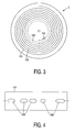
- Fig. 3 shows a disc-shaped optical record carrier 1 according to the invention.
- Recording layer of the record carrier can be inscribed optically or magneto-optically by a recording device.
- Information on the record carrier is represented by pattern of marks.
- Information is recorded in track by a recording process in which each mark is formed by one or more recording pulses of constant or varying recording power levels P.
- the recording parameters of the recording process such as the recording power level P, the number of pulses are to be tuned for the record carrier, in particular due to its material properties.
- An example of an inscribable record carrier is the known CD Write-Once.
- the record carrier has a continuous track 101 intended for recording.
- the track 101 may be spiral and in the form of an embossed groove or ridge.
- the area of the record carrier is divided in an information recording area 103 for recording user information and control area 105 for storing information relevant for recording user information.
- the control area 105 is marked by a dashed track in the fig..
- the value of optimum recording power levels P opt for recording the record carrier may be stored as a pattern of control information in the control area 105.
- the manufacturer of the record carrier 1 must record the value.
- the value may be recorded by user during, for instance, initialization of the record carrier 1, allowing the recording of a carrier-specific value.
- Fig. 4 shown a strongly enlarged portion 107 of the track comprising a pattern of marks 109 in which the control information is encoded.
Landscapes
- Physics & Mathematics (AREA)
- Optics & Photonics (AREA)
- Optical Recording Or Reproduction (AREA)
- Optical Head (AREA)
Claims (10)
- Verfahren zur Bestimmung optimierter Werte eines Parametersatzes für die Aufzeichnungsimpulsserie zum Aufzeichnen auf optischen Trägern, wobei die Aufzeichnungsimpulsserie auf eine Aufzeichnungsoberfläche eines optischen Aufzeichnungsträgers angewendet wird, um ein Muster optisch lesbarer Marken auf den Aufzeichnungsträger zu schreiben, wobei je eine Aufzeichnungsimpulsserie eine Marke bildet und das Verfahren Folgendes umfasst:- Schreiben eines Schreibtests, wobei jeder Schreibtest eine Anzahl N Testmuster umfasst, von denen jedes vorher festgelegte Werte des Parametersatzes für die Aufzeichnungsimpulsserie umfasst und diese Werte sich für jedes Testmuster unterscheiden,- Lesen des Testmusters und Bilden eines Lesesignals,- Messen der Jitter-Werte des Lesesignals, die den jeweiligen Testmustern entsprechen, und- Bestimmen der optimierten Werte des Parametersatzes für die Aufzeichnungsimpulsserie, mit denen die niedrigsten Jitter-Werte erzielt werden,dadurch gekennzeichnet, dass diese optimierten Werte bestimmt werden durch eine lineare Abhängigkeit zwischen den Werten eines Parametersatzes für die Aufzeichnungsimpulsserie und den gemessenen Jitter-Werten, die durch Differenzierung einer Gleichung erhalten werden, welche Jitter als eine Funktion des Parametersatzes für die Aufzeichnungsimpulsserie und der optimierten Werte definiert, wobei die Mindestanzahl Nmin der Testmuster von einer Anzahl P der Parameter für die Aufzeichnungsimpulsserie gemäß der Gleichung Nmin = 2*P+1 abhängt.
- Verfahren nach Anspruch 1, bei dem das Muster der optisch lesbaren Marken einer RLL-Codesequenz (Run Length Limited) entspricht.
- Verfahren nach Anspruch 1, bei dem das Testmuster eine Zufalls-RLL-Codesequenz umfasst.
- Verfahren nach Anspruch 1, bei dem der Parameter eine Strahlungsleistung von einem der Aufzeichnungsimpulse aus der Aufzeichnungsimpulsserie angibt.
- Verfahren nach Anspruch 1, bei dem der Parameter eine Breite von einem der Aufzeichnungsimpulse aus der Aufzeichnungsimpulsserie angibt.
- Verfahren nach Anspruch 1, bei dem der Satz der optimierten Werte der Parameter für die Aufzeichnungsimpulsserie auf den optischen Aufzeichnungsträger aufgezeichnet wird.
- Verfahren nach Anspruch 4 oder 5, bei dem sich die Parameter für 3T-Marken von den Parametern für längere Marken unterscheiden und bei dem T die Zeitdauer einer Periode eines Referenztakts in einem Datensignal darstellt.
- Einrichtung zur Bestimmung optimierter Werte eines Parametersatzes für die Aufzeichnungsimpulsserie zum Aufzeichnen auf optischen Trägem, wobei die Einrichtung Folgendes umfasst:- Aufzeichnungsmittel (17) zum Schreiben eines Musters optisch lesbarer Marken auf einen Aufzeichnungsträger (1) durch Bestrahlen einer Aufzeichnungsoberfläche (5) des Aufzeichnungsträgers mit Aufzeichnungsimpulsserien, wobei je eine Aufzeichnungsimpulsserie eine Marke bildet, und zum Schreiben eines Schreibtests, wobei jeder Schreibtest eine Anzahl von N Testmustern umfasst und jedes Testmuster vorher festgelegte Werte des Parametersatzes für die Aufzeichnungsimpulsserie umfasst und sich diese Werte für alle Testmuster unterscheiden,- Lesemittel (41) zum Lesen des Testsignals und zum Bilden eines Lesesignals,- einen Jitter-Detektor (51) zum Messen der Jitter-Werte des Lesesignals, die den jeweiligen Testmustern entsprechen, und zum Zuführen des Jitter-Signals an die Steuermittel,- Steuermittel (61) zum Bestimmen der optimierten Werte des Parametersatzes für die Aufzeichnungsimpulsserie, mit denen die niedrigsten Jitter-Werte erzielt werden,dadurch gekennzeichnet, dass diese Steuermittel (61) ausgebildet sind zur Anwendung einer linearen Abhängigkeit zwischen den Werten eines Parametersatzes für die Aufzeichnungsimpulsserie und den gemessenen Jitter-Werten, die durch Differenzierung einer Gleichung erhalten werden, die Jitter als Funktion des Parametersatzes für die Aufzeichnungsimpulsserie und der optimierten Werte definiert, wobei die Mindestanzahl Nmin der Testmuster von einer Anzahl P der Parameter für die Aufzeichnungsimpulsserie gemäß der Gleichung Nmin = 2*P+1 abhängt.
- Einrichtung nach Anspruch 8, die Speichermittel zum Speichern von Koeffizienten der linearen Abhängigkeit zwischen den Werten eines Parametersatzes für die Auf zeichnungsimpulsserie und den gemessenen Jitter-Werten umfasst.
- Einrichtung nach Anspruch 9 oder 10, die Speichermittel zum Speichern des Satzes der optimierten Werte des Parametersatzes für die Aufzeichnungsimpulsserie umfasst.
Priority Applications (1)
| Application Number | Priority Date | Filing Date | Title |
|---|---|---|---|
| EP03732814A EP1518231B1 (de) | 2002-06-20 | 2003-06-20 | Verfahren und vorrichtung zur bestimmung eines satzes von parametern von aufnahme-pulsen zum aufnehmen auf optischen datenträgern, und optischer datenträger |
Applications Claiming Priority (4)
| Application Number | Priority Date | Filing Date | Title |
|---|---|---|---|
| EP02077527 | 2002-06-20 | ||
| EP02077527 | 2002-06-20 | ||
| EP03732814A EP1518231B1 (de) | 2002-06-20 | 2003-06-20 | Verfahren und vorrichtung zur bestimmung eines satzes von parametern von aufnahme-pulsen zum aufnehmen auf optischen datenträgern, und optischer datenträger |
| PCT/IB2003/002394 WO2004001730A1 (en) | 2002-06-20 | 2003-06-20 | Method and device for determining a set of recording pulse series parameters for optical carrier recording and optical record carrier |
Publications (2)
| Publication Number | Publication Date |
|---|---|
| EP1518231A1 EP1518231A1 (de) | 2005-03-30 |
| EP1518231B1 true EP1518231B1 (de) | 2006-11-29 |
Family
ID=29797231
Family Applications (1)
| Application Number | Title | Priority Date | Filing Date |
|---|---|---|---|
| EP03732814A Expired - Lifetime EP1518231B1 (de) | 2002-06-20 | 2003-06-20 | Verfahren und vorrichtung zur bestimmung eines satzes von parametern von aufnahme-pulsen zum aufnehmen auf optischen datenträgern, und optischer datenträger |
Country Status (10)
| Country | Link |
|---|---|
| US (1) | US7123562B2 (de) |
| EP (1) | EP1518231B1 (de) |
| JP (1) | JP4156589B2 (de) |
| KR (1) | KR20050014868A (de) |
| CN (1) | CN1316479C (de) |
| AT (1) | ATE347165T1 (de) |
| AU (1) | AU2003240199A1 (de) |
| DE (1) | DE60310077T2 (de) |
| TW (1) | TWI302305B (de) |
| WO (1) | WO2004001730A1 (de) |
Families Citing this family (11)
| Publication number | Priority date | Publication date | Assignee | Title |
|---|---|---|---|---|
| JP2007521592A (ja) * | 2003-06-26 | 2007-08-02 | コーニンクレッカ フィリップス エレクトロニクス エヌ ヴィ | 記録可能な光ストレージシステムで最適なレーザパワーを決定する方法及び装置 |
| JP2005216347A (ja) * | 2004-01-28 | 2005-08-11 | Sony Corp | 記録パルス最適化方法 |
| CN101203910A (zh) * | 2005-03-15 | 2008-06-18 | 皇家飞利浦电子股份有限公司 | 用于确定用于在光学记录载体上记录数据的写策略参数以及用于确定用于从光学记录载体读出数据的读参数的装置和方法 |
| US7545716B2 (en) * | 2005-12-30 | 2009-06-09 | Mediatek Inc. | Optical disc drive and related method of determining optimum write power for writing data to optical disc |
| US20100020660A1 (en) * | 2007-02-13 | 2010-01-28 | Pioneer Corporation | Information recording apparatus and method, computer program, and recording medium |
| US20100020661A1 (en) * | 2007-02-13 | 2010-01-28 | Pioneer Corporation | Information recording apparatus and method, computer program, and recording medium |
| US8089843B2 (en) * | 2007-08-10 | 2012-01-03 | Sony Disc & Digital Solutions, Inc. | Recording drive waveform adjusting method for manufacturing master disc, master disc manufacturing method, master disc manufacturing apparatus, and master disc |
| KR20090065208A (ko) * | 2007-12-17 | 2009-06-22 | 삼성전자주식회사 | 디스크 구동기에서 라이트 스트래티지 파라미터 설정 방법및 그와 같은 기능을 갖는 기록 및 재생 장치 |
| US8724439B2 (en) | 2009-05-18 | 2014-05-13 | Mitsubishi Electric Corporation | Optical recording method and optical recording device |
| US9021325B2 (en) * | 2013-02-07 | 2015-04-28 | Lsi Corporation | Classifying bit errors in transmitted run length limited data |
| CN113127807B (zh) * | 2021-04-19 | 2023-02-24 | 深圳华创电科技术有限公司 | 一种基于约束最小二乘算法的Mode5前导脉冲抖动值计算方法 |
Family Cites Families (15)
| Publication number | Priority date | Publication date | Assignee | Title |
|---|---|---|---|---|
| DE3235795A1 (de) | 1982-09-28 | 1984-03-29 | Dr. Karl Thomae Gmbh, 7950 Biberach | Neues verfahren zur herstellung von 5,11-dihydro-11-((4-methyl-1-piperazinyl)- acetyl)- 6h-pyrido(2,3-b)(1,4)- benzodiazepin-6-on |
| NL9000328A (nl) * | 1989-06-23 | 1991-01-16 | Philips Nv | Werkwijze en inrichting voor het aanbrengen van informatiepatronen op een registratiedrager. |
| US5590111A (en) * | 1990-06-29 | 1996-12-31 | Hitachi, Ltd. | Method of controlling recording of optical records |
| JP2653259B2 (ja) * | 1991-03-19 | 1997-09-17 | 松下電器産業株式会社 | 記録レーザ強度設定方法及びレーザ記録装置 |
| JP3124721B2 (ja) * | 1995-09-11 | 2001-01-15 | 株式会社リコー | 光学的情報記録再生方法及び光学的情報記録再生装置 |
| JP4086913B2 (ja) * | 1995-10-09 | 2008-05-14 | 松下電器産業株式会社 | 光ディスクおよび光ディスクの再生装置 |
| US5793737A (en) * | 1996-12-06 | 1998-08-11 | U.S. Philips Corporation | Method and apparatus for writing optical recording media with optimum value of write power |
| TW382703B (en) * | 1997-03-14 | 2000-02-21 | Hitachi Ltd | Signal recording method, phase difference detecting circuit, and information apparatus |
| US6243339B1 (en) | 1997-08-12 | 2001-06-05 | U.S. Philips Corporation | Method and device for writing optical record carriers |
| WO2000028535A1 (en) * | 1998-11-06 | 2000-05-18 | Matsushita Electric Industrial Co., Ltd. | Method and device for finding conditions on recording pulse of optical disk |
| US6611481B1 (en) * | 1999-04-28 | 2003-08-26 | Matsushita Electric Industrial Co., Ltd. | Optical recording/reproducing apparatus |
| US6459666B1 (en) * | 1999-09-06 | 2002-10-01 | Ricoh Company, Ltd. | Information recording apparatus and method |
| US6807134B2 (en) * | 1999-12-28 | 2004-10-19 | Matsushita Electric Industrial Co., Ltd. | Asymmetry detection apparatus, jitter detection apparatus, and recording/reproduction apparatus |
| BR0107658B1 (pt) * | 2000-11-17 | 2014-08-12 | Koninkl Philips Electronics Nv | Métodos para ajustar um valor ótimo de um parâmetro de escrita para uso em um aparelho de gravação óptica, e de um nível de potência de escrita de um feixe de radiação, aparelho de gravação óptica para gravar informação sobre um meio de gravação óptica, e, meio de gravação óptica |
| CN1397067A (zh) * | 2000-12-04 | 2003-02-12 | 皇家菲利浦电子有限公司 | 确定最佳写功率的方法及光学记录装置 |
-
2003
- 2003-06-20 KR KR10-2004-7020706A patent/KR20050014868A/ko not_active Ceased
- 2003-06-20 AT AT03732814T patent/ATE347165T1/de not_active IP Right Cessation
- 2003-06-20 CN CNB038140470A patent/CN1316479C/zh not_active Expired - Fee Related
- 2003-06-20 EP EP03732814A patent/EP1518231B1/de not_active Expired - Lifetime
- 2003-06-20 DE DE60310077T patent/DE60310077T2/de not_active Expired - Fee Related
- 2003-06-20 TW TW092117021A patent/TWI302305B/zh active
- 2003-06-20 AU AU2003240199A patent/AU2003240199A1/en not_active Abandoned
- 2003-06-20 JP JP2004515119A patent/JP4156589B2/ja not_active Expired - Fee Related
- 2003-06-20 WO PCT/IB2003/002394 patent/WO2004001730A1/en not_active Ceased
- 2003-06-20 US US10/517,974 patent/US7123562B2/en not_active Expired - Fee Related
Also Published As
| Publication number | Publication date |
|---|---|
| JP2005530301A (ja) | 2005-10-06 |
| KR20050014868A (ko) | 2005-02-07 |
| DE60310077D1 (de) | 2007-01-11 |
| AU2003240199A1 (en) | 2004-01-06 |
| US20050232106A1 (en) | 2005-10-20 |
| TWI302305B (en) | 2008-10-21 |
| EP1518231A1 (de) | 2005-03-30 |
| US7123562B2 (en) | 2006-10-17 |
| WO2004001730A1 (en) | 2003-12-31 |
| JP4156589B2 (ja) | 2008-09-24 |
| ATE347165T1 (de) | 2006-12-15 |
| DE60310077T2 (de) | 2007-06-21 |
| CN1662971A (zh) | 2005-08-31 |
| TW200415593A (en) | 2004-08-16 |
| CN1316479C (zh) | 2007-05-16 |
Similar Documents
| Publication | Publication Date | Title |
|---|---|---|
| KR100455717B1 (ko) | 시험삼아 써보기방법 및 이것을 이용한 광디스크장치 | |
| US6611481B1 (en) | Optical recording/reproducing apparatus | |
| WO1998025267A1 (en) | Method and apparatus for writing optical recording media | |
| EP1518231B1 (de) | Verfahren und vorrichtung zur bestimmung eines satzes von parametern von aufnahme-pulsen zum aufnehmen auf optischen datenträgern, und optischer datenträger | |
| EP1519365B1 (de) | Verfahren und Vorrichtung zur optischen Aufnahme und Wiedergabe | |
| US6842413B2 (en) | Method of calculating write condition detection index and optical disk writing method and apparatus using the method | |
| JP4971509B2 (ja) | 記録パワー決定方法、プログラムおよび記録媒体 | |
| US7522509B2 (en) | Semiconductor laser driving device and optical disc device | |
| US7693015B2 (en) | Optical information recording device, optical information recording method, and signal processing circuit | |
| JP2000507027A (ja) | 光学的記録方法及び該方法を使用する装置 | |
| KR100731781B1 (ko) | 광정보기록장치 | |
| JP4268312B2 (ja) | 光学的記録再生装置 | |
| US20100238776A1 (en) | Method of optimizing the write power for recording marks in an information layer of a record carrier and recording device using such an optimizing method | |
| KR100516813B1 (ko) | 광기록매체의기록방법및장치 | |
| US8064303B2 (en) | Analysis of optical effects on storage medium | |
| EP1568019B1 (de) | Bestimmung eines werts eines aufzeichnungsimpulsparameters für die optische aufzeichnung | |
| US20070263513A1 (en) | Optical disk recording device, recording method for optical disk | |
| US20020031068A1 (en) | Method and apparatus for writing optical recording media | |
| US20060198262A1 (en) | Optical recording apparatus and optical recording method controlling laser power for disc overwriting | |
| US5719838A (en) | β compensation using a defocus technique | |
| KR20060030054A (ko) | 기록가능한 광학 기록 시스템에서 최적의 레이저 전력을결정하기 위한 장치 및 방법 | |
| RU2375765C2 (ru) | Способ и устройство определения мощности записи | |
| EP0916132A2 (de) | Verfahren und vorrichtung zum beschreiben optischer aufzeichnungsträger |
Legal Events
| Date | Code | Title | Description |
|---|---|---|---|
| PUAI | Public reference made under article 153(3) epc to a published international application that has entered the european phase |
Free format text: ORIGINAL CODE: 0009012 |
|
| 17P | Request for examination filed |
Effective date: 20050120 |
|
| AK | Designated contracting states |
Kind code of ref document: A1 Designated state(s): AT BE BG CH CY CZ DE DK EE ES FI FR GB GR HU IE IT LI LU MC NL PT RO SE SI SK TR |
|
| AX | Request for extension of the european patent |
Extension state: AL LT LV MK |
|
| DAX | Request for extension of the european patent (deleted) | ||
| GRAP | Despatch of communication of intention to grant a patent |
Free format text: ORIGINAL CODE: EPIDOSNIGR1 |
|
| GRAJ | Information related to disapproval of communication of intention to grant by the applicant or resumption of examination proceedings by the epo deleted |
Free format text: ORIGINAL CODE: EPIDOSDIGR1 |
|
| GRAP | Despatch of communication of intention to grant a patent |
Free format text: ORIGINAL CODE: EPIDOSNIGR1 |
|
| GRAS | Grant fee paid |
Free format text: ORIGINAL CODE: EPIDOSNIGR3 |
|
| GRAA | (expected) grant |
Free format text: ORIGINAL CODE: 0009210 |
|
| AK | Designated contracting states |
Kind code of ref document: B1 Designated state(s): AT BE BG CH CY CZ DE DK EE ES FI FR GB GR HU IE IT LI LU MC NL PT RO SE SI SK TR |
|
| PG25 | Lapsed in a contracting state [announced via postgrant information from national office to epo] |
Ref country code: IT Free format text: LAPSE BECAUSE OF FAILURE TO SUBMIT A TRANSLATION OF THE DESCRIPTION OR TO PAY THE FEE WITHIN THE PRESCRIBED TIME-LIMIT;WARNING: LAPSES OF ITALIAN PATENTS WITH EFFECTIVE DATE BEFORE 2007 MAY HAVE OCCURRED AT ANY TIME BEFORE 2007. THE CORRECT EFFECTIVE DATE MAY BE DIFFERENT FROM THE ONE RECORDED. Effective date: 20061129 Ref country code: BE Free format text: LAPSE BECAUSE OF FAILURE TO SUBMIT A TRANSLATION OF THE DESCRIPTION OR TO PAY THE FEE WITHIN THE PRESCRIBED TIME-LIMIT Effective date: 20061129 Ref country code: AT Free format text: LAPSE BECAUSE OF FAILURE TO SUBMIT A TRANSLATION OF THE DESCRIPTION OR TO PAY THE FEE WITHIN THE PRESCRIBED TIME-LIMIT Effective date: 20061129 Ref country code: SI Free format text: LAPSE BECAUSE OF FAILURE TO SUBMIT A TRANSLATION OF THE DESCRIPTION OR TO PAY THE FEE WITHIN THE PRESCRIBED TIME-LIMIT Effective date: 20061129 Ref country code: NL Free format text: LAPSE BECAUSE OF FAILURE TO SUBMIT A TRANSLATION OF THE DESCRIPTION OR TO PAY THE FEE WITHIN THE PRESCRIBED TIME-LIMIT Effective date: 20061129 Ref country code: CH Free format text: LAPSE BECAUSE OF FAILURE TO SUBMIT A TRANSLATION OF THE DESCRIPTION OR TO PAY THE FEE WITHIN THE PRESCRIBED TIME-LIMIT Effective date: 20061129 Ref country code: FI Free format text: LAPSE BECAUSE OF FAILURE TO SUBMIT A TRANSLATION OF THE DESCRIPTION OR TO PAY THE FEE WITHIN THE PRESCRIBED TIME-LIMIT Effective date: 20061129 Ref country code: SK Free format text: LAPSE BECAUSE OF FAILURE TO SUBMIT A TRANSLATION OF THE DESCRIPTION OR TO PAY THE FEE WITHIN THE PRESCRIBED TIME-LIMIT Effective date: 20061129 Ref country code: CZ Free format text: LAPSE BECAUSE OF FAILURE TO SUBMIT A TRANSLATION OF THE DESCRIPTION OR TO PAY THE FEE WITHIN THE PRESCRIBED TIME-LIMIT Effective date: 20061129 Ref country code: LI Free format text: LAPSE BECAUSE OF FAILURE TO SUBMIT A TRANSLATION OF THE DESCRIPTION OR TO PAY THE FEE WITHIN THE PRESCRIBED TIME-LIMIT Effective date: 20061129 Ref country code: RO Free format text: LAPSE BECAUSE OF FAILURE TO SUBMIT A TRANSLATION OF THE DESCRIPTION OR TO PAY THE FEE WITHIN THE PRESCRIBED TIME-LIMIT Effective date: 20061129 |
|
| REG | Reference to a national code |
Ref country code: GB Ref legal event code: FG4D |
|
| REG | Reference to a national code |
Ref country code: CH Ref legal event code: EP |
|
| REG | Reference to a national code |
Ref country code: IE Ref legal event code: FG4D |
|
| REF | Corresponds to: |
Ref document number: 60310077 Country of ref document: DE Date of ref document: 20070111 Kind code of ref document: P |
|
| PG25 | Lapsed in a contracting state [announced via postgrant information from national office to epo] |
Ref country code: BG Free format text: LAPSE BECAUSE OF FAILURE TO SUBMIT A TRANSLATION OF THE DESCRIPTION OR TO PAY THE FEE WITHIN THE PRESCRIBED TIME-LIMIT Effective date: 20070228 Ref country code: DK Free format text: LAPSE BECAUSE OF FAILURE TO SUBMIT A TRANSLATION OF THE DESCRIPTION OR TO PAY THE FEE WITHIN THE PRESCRIBED TIME-LIMIT Effective date: 20070228 Ref country code: SE Free format text: LAPSE BECAUSE OF FAILURE TO SUBMIT A TRANSLATION OF THE DESCRIPTION OR TO PAY THE FEE WITHIN THE PRESCRIBED TIME-LIMIT Effective date: 20070228 |
|
| PG25 | Lapsed in a contracting state [announced via postgrant information from national office to epo] |
Ref country code: ES Free format text: LAPSE BECAUSE OF FAILURE TO SUBMIT A TRANSLATION OF THE DESCRIPTION OR TO PAY THE FEE WITHIN THE PRESCRIBED TIME-LIMIT Effective date: 20070312 |
|
| PG25 | Lapsed in a contracting state [announced via postgrant information from national office to epo] |
Ref country code: PT Free format text: LAPSE BECAUSE OF FAILURE TO SUBMIT A TRANSLATION OF THE DESCRIPTION OR TO PAY THE FEE WITHIN THE PRESCRIBED TIME-LIMIT Effective date: 20070430 |
|
| NLV1 | Nl: lapsed or annulled due to failure to fulfill the requirements of art. 29p and 29m of the patents act | ||
| ET | Fr: translation filed | ||
| REG | Reference to a national code |
Ref country code: CH Ref legal event code: PL |
|
| PLBE | No opposition filed within time limit |
Free format text: ORIGINAL CODE: 0009261 |
|
| STAA | Information on the status of an ep patent application or granted ep patent |
Free format text: STATUS: NO OPPOSITION FILED WITHIN TIME LIMIT |
|
| 26N | No opposition filed |
Effective date: 20070830 |
|
| PG25 | Lapsed in a contracting state [announced via postgrant information from national office to epo] |
Ref country code: MC Free format text: LAPSE BECAUSE OF NON-PAYMENT OF DUE FEES Effective date: 20070630 |
|
| PG25 | Lapsed in a contracting state [announced via postgrant information from national office to epo] |
Ref country code: GR Free format text: LAPSE BECAUSE OF FAILURE TO SUBMIT A TRANSLATION OF THE DESCRIPTION OR TO PAY THE FEE WITHIN THE PRESCRIBED TIME-LIMIT Effective date: 20070301 |
|
| PG25 | Lapsed in a contracting state [announced via postgrant information from national office to epo] |
Ref country code: IE Free format text: LAPSE BECAUSE OF NON-PAYMENT OF DUE FEES Effective date: 20070620 |
|
| PGFP | Annual fee paid to national office [announced via postgrant information from national office to epo] |
Ref country code: DE Payment date: 20080808 Year of fee payment: 6 |
|
| PGFP | Annual fee paid to national office [announced via postgrant information from national office to epo] |
Ref country code: FR Payment date: 20080626 Year of fee payment: 6 |
|
| PGFP | Annual fee paid to national office [announced via postgrant information from national office to epo] |
Ref country code: GB Payment date: 20080805 Year of fee payment: 6 |
|
| PG25 | Lapsed in a contracting state [announced via postgrant information from national office to epo] |
Ref country code: EE Free format text: LAPSE BECAUSE OF FAILURE TO SUBMIT A TRANSLATION OF THE DESCRIPTION OR TO PAY THE FEE WITHIN THE PRESCRIBED TIME-LIMIT Effective date: 20061129 |
|
| PG25 | Lapsed in a contracting state [announced via postgrant information from national office to epo] |
Ref country code: LU Free format text: LAPSE BECAUSE OF NON-PAYMENT OF DUE FEES Effective date: 20070620 Ref country code: CY Free format text: LAPSE BECAUSE OF FAILURE TO SUBMIT A TRANSLATION OF THE DESCRIPTION OR TO PAY THE FEE WITHIN THE PRESCRIBED TIME-LIMIT Effective date: 20061129 |
|
| PG25 | Lapsed in a contracting state [announced via postgrant information from national office to epo] |
Ref country code: HU Free format text: LAPSE BECAUSE OF FAILURE TO SUBMIT A TRANSLATION OF THE DESCRIPTION OR TO PAY THE FEE WITHIN THE PRESCRIBED TIME-LIMIT Effective date: 20070530 Ref country code: TR Free format text: LAPSE BECAUSE OF FAILURE TO SUBMIT A TRANSLATION OF THE DESCRIPTION OR TO PAY THE FEE WITHIN THE PRESCRIBED TIME-LIMIT Effective date: 20061129 |
|
| GBPC | Gb: european patent ceased through non-payment of renewal fee |
Effective date: 20090620 |
|
| REG | Reference to a national code |
Ref country code: FR Ref legal event code: ST Effective date: 20100226 |
|
| PG25 | Lapsed in a contracting state [announced via postgrant information from national office to epo] |
Ref country code: FR Free format text: LAPSE BECAUSE OF NON-PAYMENT OF DUE FEES Effective date: 20090630 |
|
| PG25 | Lapsed in a contracting state [announced via postgrant information from national office to epo] |
Ref country code: GB Free format text: LAPSE BECAUSE OF NON-PAYMENT OF DUE FEES Effective date: 20090620 |
|
| PG25 | Lapsed in a contracting state [announced via postgrant information from national office to epo] |
Ref country code: DE Free format text: LAPSE BECAUSE OF NON-PAYMENT OF DUE FEES Effective date: 20100101 |