EP1516904A2 - Strahlungsbildwandler und Verfahren zu seiner Herstellung - Google Patents
Strahlungsbildwandler und Verfahren zu seiner Herstellung Download PDFInfo
- Publication number
- EP1516904A2 EP1516904A2 EP04021794A EP04021794A EP1516904A2 EP 1516904 A2 EP1516904 A2 EP 1516904A2 EP 04021794 A EP04021794 A EP 04021794A EP 04021794 A EP04021794 A EP 04021794A EP 1516904 A2 EP1516904 A2 EP 1516904A2
- Authority
- EP
- European Patent Office
- Prior art keywords
- stimulable phosphor
- radiation image
- support
- image conversion
- phosphor layer
- Prior art date
- Legal status (The legal status is an assumption and is not a legal conclusion. Google has not performed a legal analysis and makes no representation as to the accuracy of the status listed.)
- Withdrawn
Links
Images

Classifications
-
- C—CHEMISTRY; METALLURGY
- C09—DYES; PAINTS; POLISHES; NATURAL RESINS; ADHESIVES; COMPOSITIONS NOT OTHERWISE PROVIDED FOR; APPLICATIONS OF MATERIALS NOT OTHERWISE PROVIDED FOR
- C09K—MATERIALS FOR MISCELLANEOUS APPLICATIONS, NOT PROVIDED FOR ELSEWHERE
- C09K11/00—Luminescent materials, e.g. electroluminescent or chemiluminescent
- C09K11/08—Luminescent materials, e.g. electroluminescent or chemiluminescent containing inorganic luminescent materials
- C09K11/77—Luminescent materials, e.g. electroluminescent or chemiluminescent containing inorganic luminescent materials containing rare earth metals
- C09K11/7728—Luminescent materials, e.g. electroluminescent or chemiluminescent containing inorganic luminescent materials containing rare earth metals containing europium
- C09K11/7732—Halogenides
- C09K11/7733—Halogenides with alkali or alkaline earth metals
-
- G—PHYSICS
- G21—NUCLEAR PHYSICS; NUCLEAR ENGINEERING
- G21K—HANDLING OF PARTICLES OR IONISING RADIATION NOT OTHERWISE PROVIDED FOR; IRRADIATION DEVICES; GAMMA RAY OR X-RAY MICROSCOPES
- G21K4/00—Conversion screens for the conversion of the spatial distribution of X-rays or particle radiation into visible images, e.g. fluoroscopic screens
Definitions
- the present invention relates to a radiation image conversion panel comprising a stimulable phosphor layer which has been formed by a process of gas-phase deposition, and a preparation method thereof.
- This radiation image conversion method is a process in which radiation rays having transmitted a subject are exposed onto the stimulable phosphor layer, whereby radiation energy corresponding to the radiation transmission density of the respective portions of the subject is accumulated in a stimulable phosphor, thereafter, the radiation energy accumulated in the stimulable phosphor is emitted as photo-stimulated luminescence by excitation of stimulating light and the strength of the stimulated luminescence is converted to an electric signal, which is further converted to a visible image through imaging materials such as photographic material or an image display such as a CRT (Cathode Ray Tube) or a LCD (liquid Crystal Display).
- CTR Cathode Ray Tube
- LCD liquid Crystal Display
- JP-A No. 5-249298 JP-A No. 5-249298
- AX type phosphor which comprise the parent alkali halide such as CsBr and an activator such as Eu, exhibit relatively high thermal expansion coefficient and enhancing crystallinity results in a tendency of peeling off from the support and reduced shock resistance. Accordingly, not only enhanced sensitivity and superior sharpness but also enhanced resistance to peeling or shock are required in the stimulable phosphor layer.
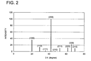
- the invention is directed to a radiation image conversion panel comprising a stimulable phosphor layer, characterized in that when subjected to powder X-ray diffractometry at incident angles within the range of from 10° to 70°, the stimulable phosphor layer exhibits an X-ray diffraction pattern meeting the following requirement: 0.3 ⁇ I 2 /I 1 ⁇ 1.0 wherein I 1 is a first peak intensity and I 2 is a second peak intensity when subjected to powder X-ray diffractometry at incident angles within the range of from 10° to 70°.
- the invention is directed to a method of preparing the radiation image conversion panel described above, comprising forming a stimulable phosphor layer comprised of a stimulable phosphor deposited on a support by a process of gas phase deposition using a vacuum deposition apparatus.
- a radiation image conversion panel comprises a support (11) provided thereon with a stimulable phosphor layer (12) comprising a stimulable phosphor formed of columnar crystals (12a).
- the columnar crystals are formed by crystal growth of a stimulable phosphor through gas phase deposition.
- the support (11) which can be optimally chosen from commonly known materials used for a support of conventional radiation image conversion panels, preferably is a quartz glass sheet, a sheet of metal such as aluminum, iron, tin, or chromium or a carbon fiber-reinforced resin sheet in terms of forming the stimulable phosphor layer (12) by a process of gas phase deposition.
- the support (11) preferably has a resin layer to smoothen the surface thereof.
- the resin layer preferably contains compounds such as polyimide, polyethylene terephthalate, paraffin and graphite and the layer thickness is preferably 5 ⁇ m to 50 ⁇ m.
- the resin layer may be provided on the surface of the support, the opposite side or both sides thereof.
- Means for providing a resin layer on the support (11) include, for example, a pasting method and a coating method. In the pasting method, a pressure roller is employed, in which heating is made preferably at a temperature of 80 to 150 °C under a pressure of 4.90x10 to 2.94x10 2 N/cm at a transporting speed of 0.1 to 2.0 m/sec.
- the stimulable phosphor layer is comprised of a stimulable phosphor formed of columnar crystals.
- the stimulable phosphor layer is formed by depositing the stimulable phosphor in the gas phase on the support to grow the phosphor crystals in a columnar form.
- the direction of a crystal lattice plane is controlled so that the stimulable phosphor layer exhibits an X-ray diffraction pattern meeting the following requirement: 0.3 ⁇ I 2 /I 1 ⁇ 1.0 wherein I 1 is the first peak intensity and I 2 is the second peak intensity, when subjected to powder X-ray diffractometry at X-ray incident angles over a range of 10° to 70°.
- the X-ray incident angle refers to an acute angle ( ⁇ ) between the direction of an incident X-ray and a plane perpendicular to the direction of the highest growth rate in the formation of the stimulable phosphor layer (12).
- the first peak intensity (I 1 ) refers to the intensity of a peak exhibiting the maximum (or highest) intensity in an X-ray diffraction pattern obtained when an X-ray is allowed to enter the stimulable phosphor layer (12) at a prescribed incident angle ( ⁇ ) from an X-ray source, and the quantity of an X-ray which reaches an X-ray detector is measured.
- the second peak intensity (I) refers to the intensity of the peak exhibiting the second highest intensity. In the case of being synonymous with each other as a crystal plane, for example, a (100) plane and a (200) plane, they are treated as distinct peaks.
- X-rays usable in this invention include, for example, CuK ⁇ (1.54 ⁇ ).
- the stimulable phosphor layer is subjected to powder X-ray diffractometry at X-ray incident angles over a range of 10° to 70° with respect to the crystal lattice plane normal to the direction of the highest growth rate.
- the direction of the highest growth rate during the formation of the stimulable phosphor layer refers to the direction of growing the columnar crystals or the direction of the columnar crystals being elongated.
- the direction of the highest growth rate is usually a direction perpendicular to the surface of the support (11), as shown in Fig. 1(a), in which the highest growth rate of columnar phosphor crystals is in the direction indicated by the arrow "A".
- the crystal lattice plane exhibiting the first peak preferably is a (x00) plane, in which x is 1, 2 or 3 (preferably 1 or 2).
- the highest peak is assigned to the foregoing lattice plane (x00), in which x is 1, 2 or 3 (preferably 1 or 2).
- Fig. 2 illustrates an X-ray diffraction pattern relating to this invention.
- Such stimulable phosphor layer (12) preferably contains a stimulable phosphor comprised of an alkali halide as a parent, which is represented by the following formula (1): M 1 X ⁇ aM 2 X' 2 ⁇ bM 3 X" 3 : eA wherein M 1 represents an alkali metal selected from the group consisting of Li, Na, K, Rb and Cs; M 2 represents a divalent metal selected from the group consisting of Be, Mg, Ca, Sr, Ba, Zn, Cd, Cu and Ni; M 3 represents a trivalent metal atom selected from the group consisting of Sc, Y, La, Ce, Pr, Nd, Pm, Sm, Eu, Gd, Tb, Dy, Ho, Er, Tm, Yb, Lu, Al, Ga and In; X, X' and X" each represent a halogen atom selected from the group consisting of F, Cl, Br and I; A represents a metal selected from the group consisting of Eu, Tb, In,
- M 1 is an alkali metal selected from the group consisting of Li, Na, K, Rb and Cs, preferably an alkali metal selected from the group consisting of Rb and Cs, and more preferably a Cs atom.
- M 2 is a divalent metal selected from the group consisting of Be, Mg, Ca, Sr, Ba, Zn, Cd, Cu and Ni; and preferably a divalent metal selected from the group consisting of Be, Mg, Ca, Sr and Ba.
- M 3 is a trivalent metal atom selected from the group consisting of Sc, Y, La, Ce, Pr, Nd, Pm, Sm, Eu, Gd, Tb, Dy, Ho, Er, Tm, Yb, Lu, Al, Ga and In; and preferably a trivalent metal atom selected from the group consisting of Y, Ce, Sm, Eu, Al, La, Gd, Lu, Ga and In.
- A is a metal selected from the group consisting of Eu, Tb, In, Ce, Tm, Dy, Pr, Ho, Nd, Yb, Er, Gd, Lu, Sm, Y, Tl, Na, Ag, Cu and Mg; of these, Eu atom is preferred.
- X, X' and X" each represent a halogen atom selected from the group consisting of F, Cl, Br and I; a halogen atom selected from the group consisting of F, Cl and Br is preferred and Br atom is more preferred.
- b is 0 ⁇ b ⁇ 0.5 and preferably 0 ⁇ b ⁇ 10 -2 .
- Stimulable phosphors of the foregoing formula (1) can be prepared from the following raw materials (a) to (c) according to the procedure described below:
- phosphor raw materials are optimally chosen from the foregoing (a) to (c), weighed so as to satisfy the numerical range of "a", "b” and “e” of the foregoing formula (1), and then dissolved.
- a prescribed amount of an acid is added to adjust a pH value (C) of the thus obtained solution so as to fall within the range of 0 ⁇ C ⁇ 7, and then water is evaporated.
- the obtained raw material mixture is charged into a heat-resistant vessel such as a silica crucible or an alumina crucible and then placed in an electric furnace to be calcined.
- the calcination temperature preferably is 500 to 1000 °C.
- the calcination time depending on the charged amount of raw materials, calcination temperature and the like, preferably is 0.5 to 6 hrs.
- a weakly reducible atmosphere such as a nitrogen gas atmosphere containing a small amount of hydrogen gas or a carbon dioxide atmosphere containing carbon monoxide, a nitrogen gas atmosphere, a neutral atmosphere such as an argon gas atmosphere, or a trace amount of oxygen-introduced weakly oxidizing atmosphere.
- calcined material is taken out of the electric furnace and pulverized. Thereafter, powdered calcined material may again be charged into a heat resistant vessel and then placed in an electric furnace to be recalcined under the foregoing condition to further enhance emission luminance of the phosphor.
- the intended phosphor can be obtained by taking out the calcined material from the electric furnace and allowing it to stand in an aerial atmosphere.
- the calcined material may also be cooled in the same atmosphere as in the calcination, such as a weakly reducing atmosphere or a neutral atmosphere.
- the calcined material is moved from a heating section to a cooling section within the electric furnace, followed by rapidly cooling in a weakly reducing atmosphere, neutral atmosphere or weakly oxidizing atmosphere, thereby leading to further enhanced stimulated emission luminance of the phosphor.
- the stimulable phosphor layer (12) can be formed by depositing the stimulable phosphor on one side of the support (11) by applying gas phase deposition methods to grow columnar phosphor crystals until reaching a desired layer thickness.
- the gas phase deposition methods usable in this invention include a vacuum deposition method (or vacuum evaporation method), a sputter deposition method, a CVD method, an ion plating method and other appropriate methods. Of these, the vacuum deposition method is preferred.
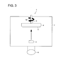
- Vacuum deposition can be performed using, for example, a vacuum deposition apparatus (1) shown in Fig. 3.
- the vacuum deposition apparatus (1) is provided with a vacuum vessel (2) and a vacuum pump (6) to evacuate the inside of the vacuum vessel (12) and to introduce atmospheric air; the interior of the vacuum vessel (2) is provided with an evaporation source (3) to evaporate or sublimate a stimulable phosphor by heating to deposit the resulting vapor onto a support (11), a support holder (4) to hold the support (11) and a support rotation mechanism (5) to rotate the support holder (4) to the evaporation source (3).
- a vapor evaporated from the evaporation source (3) is deposited onto the support (11) with rotating the support holder (4) by the support rotation mechanism (5) to form the stimulable phosphor layer (12).
- the evaporation source (3) may be composed of an aluminum crucible wound by a heater, or a boat or a heater of a high-melting metal. Besides the resistance heating method, electron beam heating or high-frequency induction heating is also applicable to heat the stimulable phosphor. Specifically, the resistance heating method is preferred in terms of being a relatively simple constitution, ease of handling and low price, and being applicable to a large number of materials. Further, the evaporation source (3) may be a molecular beam source using a molecular source epitaxial method.
- a shutter between the support (11) and the evaporation source (3) to shield a space of from the evaporation source (3) to the support (11). Proving the shutter prevents an unintended material adhered onto the stimulable phosphor surface being evaporated at the initial stage of evaporation and its adherence to the support (11).
- the support holder (4) is preferably provided with a heater to heat the support (11). Heating the surface of the support (11) can separate or remove material adsorbed onto the support surface, and preventing generation of an impurity layer between the support surface and the stimulable phosphor, promoting closer contact and optimizing film characteristics of the stimulable phosphor layer.
- the support rotation mechanism (5) is composed of, for example, a rotating shaft (5a) which rotates a support holder (4) while holding the support holder (4) and a motor (not shown in Fig. 3) which is arranged outside the vacuum vessel (2) and acts as a driving source for the rotating shaft.
- a stimulable phosphor layer (12) can be formed on a support (11), according to the following procedure.
- the support (11) is mounted on the support holder (4).
- the interior of the vacuum vessel is evacuated and regulated to the intended degree of vacuum.
- the support holder is rotated toward the evaporation source (3) by the support rotation mechanism (5).
- a stimulable phosphor is evaporated from the heated evaporation source (3) and deposits on the surface of the support (11) to grow the phosphor to the intended thickness.
- the spacing between the support (11) and the evaporation source (3) preferably is 100 mm to 1500 mm.
- the vacuum vessel is maintained at a vacuum pressure of 1x10 -3 to 1x10 0 pa, and preferably 3x10 -3 to 3x10 -1 Pa.
- the foregoing deposition process may be divided to plural times to form a stimulable phosphor layer (12). Further, using plural resistance heaters or electron beams in the deposition process, co-deposition can be performed to form the stimulable phosphor layer (12) concurrently with synthesis of an intended stimulable phosphor on the support (11).
- the substrate such as support (11), protective layer or an interlayer] may optionally be cooled or heated during deposition. After completion of the deposition, the stimulable phosphor layer (12) may optionally be heated. Further, there may be conducted vacuum deposition in which gases such as O 2 or H 2 are introduced during deposition.
- the thickness of the stimulable phosphor layer (12), depending on the objective of a radiation image conversion panel or the kind of a stimulable phosphor, is preferably 50 to 2000 ⁇ m, more preferably 50 to 1000 ⁇ m, and still more preferably 100 to 800 ⁇ m to achieve the effects of this invention.
- the support is preferably maintained at a temperature of room temperature (rt) to 300 °C, and more preferably 50 to 200 °C during the formation of the stimulable phosphor layer (12).
- adjustments of the degree of vacuum of the deposition apparatus (1), the temperature of the support (11), the deposition rate and the direction of vapor stream from the evaporation source to the surface of the support (11) can control the value of a ratio of the second peak intensity (I 2 ) to the first peak intensity (I 1 ), that is, I 2 /I 1 .
- a protective layer may optionally be provided on a side of the stimulable phosphor layer (12) opposite the support (11) to physically or chemically protect the stimulable phosphor layer (12).
- the protective layer may be formed by coating a coating solution as a protective layer on the surface of the stimulable phosphor layer (12) or by allowing a protective layer previously formed to adhere onto the stimulable phosphor layer (12). Materials used for the protective layer include those which are typically used for protective layers.
- Examples thereof include cellulose acetate, nitrocellulose, polymethyl methacrylate, polyvinyl butyral, polyvinyl formal, polycarbonate, polyester, polyethylene terephthalate, polyethylene, polyvinylidene chloride, nylon, polytetrafluoroethylene, polytrifluoroethylene, copolymer of terafluoroethylene and hexafluoropropylene, copolymer of vinylidene chloride and vinyl chloride, and copolymer of vinylidene chloride and acrylonitrile.
- a transparent glass substrate may be used as a support.
- inorganic material such as SiC, SiO 2 SiN, and Al 2 O 3 may be allowed to deposit by means of the vacuum evaporation or sputtering method to form the protective layer.
- the thickness of a protective layer is preferably 0.1 to 2,000 ⁇ m.
- a stimulable phosphor (CsBr: 0.002Eu) was deposited on one side of support (11) formed of a carbon fiber reinforced resin to form a stimulable phosphor layer (12), according to the following procedure.
- the stimulable phosphor (CsBr: 0.002Eu) was filled into a resistance heating crucible, a support (11) is set on a rotating support holder (4) and the spacing between the support (11) and a evaporation source (3) was adjusted to 500 nm.
- the inside of the deposition apparatus (1) was evacuated, then, Ar gas was introduced therein and the vacuum pressure was adjusted to a pressure of 5.0x10 -3 Pa, and thereafter the support (11) was maintained at a temperature of 100 °C while rotating the support (11) at a rate of 10 rpm. Then, the resistance heating crucible was heated to deposit the stimulable phosphor and vacuum deposition was stopped when the thickness of a stimulable phosphor layer (12) reached 500 ⁇ m. Subsequently, the stimulable phosphor layer (12) was put into a protective layer bag in a dry air atmosphere to obtain a radiation image conversion panel, as Example 1 relating to this invention, having a structure in which the stimulable phosphor layer was closely shielded.
- Example 2 to 4 Radiation image conversion panels of Example 2 to 4 were prepared similarly to Example 1, provided that the degree of vacuum inside the deposition apparatus (1) was respectively changed to pressures of 1.0x10 -2 Pa 5.0x10 -2 Pa and 1.0x10 -1 Pa as shown in Table 1.
- Example 1 to 4 and Comparative Example 1 and 2 were each measured with respect to diffraction pattern of the crystal lattice plane perpendicular to the direction of the highest growth rate at incident angles ranging from 10° to 70° to determine a ratio (I 2 /I 1 ) of the second peak intensity (I 2 ) to the first peak intensity (I 1 ) in the respective diffraction patterns. Results thereof are shown in Table 1, in which crystal lattice planes of the first peak intensities of Examples 1 to 4 and Comparative Examples 1 and 2 were each a (200) plane.
- the phosphor layer side of the panel was irradiated with semiconductor laser light (690 nm, a power of 40 mW on the panel) and the CTF chart was scanned with a semiconductor laser light beam (oscillation wavelength: 780 nm, beam diameter: 100 ⁇ m) to perform stimulation and the CTF chart image was read as stimulated emission radiated from the stimulable phosphor layer and photo-electrically converted by a photo-detector (photomultiplier) to obtain image signals. Based on these signal values, the modulation transfer function (MTF) of the image was determined. Sharpness of the radiation image was represented by a relative value, based on that of the radiation image conversion panel of Comparative Example 1 being 100. The MTF is a value at a space frequency of 1 cycle/mm. Results thereof are shown in Table 1.
- Radiation image conversion panel Examples 1 to 4 and Comparative Examples 1 and 2 were visually evaluated after a 500 g iron ball was dropped onto the respective panels. Further, the respective radiation image conversion panels were each exposed to X-rays at a bulb voltage of 80 k Vp and then scanned with a He-Ne laser (633 nm) for stimulation. Stimulated emission radiated from the phosphor layer was received by the photo-receiver described above and converted to electric signals, which were reproduced as an image by an image reproduction apparatus and printed out using an outputting apparatus. The thus obtained printed image was visually evaluated as a measure of shock resistance. Results thereof are shown in Table 1.
- Shock resistance was visually evaluated based on the following criteria:
Landscapes
- Chemical & Material Sciences (AREA)
- Engineering & Computer Science (AREA)
- Inorganic Chemistry (AREA)
- Materials Engineering (AREA)
- Organic Chemistry (AREA)
- Physics & Mathematics (AREA)
- General Engineering & Computer Science (AREA)
- High Energy & Nuclear Physics (AREA)
- Conversion Of X-Rays Into Visible Images (AREA)
- Luminescent Compositions (AREA)
Applications Claiming Priority (2)
| Application Number | Priority Date | Filing Date | Title |
|---|---|---|---|
| JP2003326115 | 2003-09-18 | ||
| JP2003326115 | 2003-09-18 |
Publications (2)
| Publication Number | Publication Date |
|---|---|
| EP1516904A2 true EP1516904A2 (de) | 2005-03-23 |
| EP1516904A3 EP1516904A3 (de) | 2005-06-01 |
Family
ID=34191346
Family Applications (1)
| Application Number | Title | Priority Date | Filing Date |
|---|---|---|---|
| EP04021794A Withdrawn EP1516904A3 (de) | 2003-09-18 | 2004-09-14 | Strahlungsbildwandler und Verfahren zu seiner Herstellung |
Country Status (2)
| Country | Link |
|---|---|
| US (1) | US7081333B2 (de) |
| EP (1) | EP1516904A3 (de) |
Families Citing this family (3)
| Publication number | Priority date | Publication date | Assignee | Title |
|---|---|---|---|---|
| WO2007060813A1 (ja) * | 2005-11-22 | 2007-05-31 | Konica Minolta Medical & Graphic, Inc. | シンチレータプレート |
| JPWO2007060814A1 (ja) * | 2005-11-28 | 2009-05-07 | コニカミノルタエムジー株式会社 | 放射線用シンチレータプレート |
| JPWO2008026453A1 (ja) * | 2006-08-30 | 2010-01-21 | コニカミノルタエムジー株式会社 | シンチレータプレート、その製造方法及び放射線イメージセンサ |
Family Cites Families (6)
| Publication number | Priority date | Publication date | Assignee | Title |
|---|---|---|---|---|
| JP3130632B2 (ja) * | 1992-03-05 | 2001-01-31 | コニカ株式会社 | 放射線画像変換パネル |
| JP2002181997A (ja) * | 2000-12-14 | 2002-06-26 | Fuji Photo Film Co Ltd | 放射線像変換パネルおよび放射線画像情報読取方法 |
| US20040016890A1 (en) * | 2002-07-25 | 2004-01-29 | Konica Corporation | Radiation image conversation panel and preparation method thereof |
| US20040159801A1 (en) * | 2003-01-09 | 2004-08-19 | Konica Minolta Holdings, Inc. | Radiographic image conversion panel |
| US7029836B2 (en) * | 2003-02-10 | 2006-04-18 | Konica Minolta Holdings, Inc. | Radiographic image conversion panel and method for manufacturing the same |
| JP3987463B2 (ja) * | 2003-06-16 | 2007-10-10 | 富士フイルム株式会社 | 放射線像変換パネル |
-
2004
- 2004-09-14 EP EP04021794A patent/EP1516904A3/de not_active Withdrawn
- 2004-09-16 US US10/942,025 patent/US7081333B2/en not_active Expired - Fee Related
Also Published As
| Publication number | Publication date |
|---|---|
| EP1516904A3 (de) | 2005-06-01 |
| US20050061993A1 (en) | 2005-03-24 |
| US7081333B2 (en) | 2006-07-25 |
Similar Documents
| Publication | Publication Date | Title |
|---|---|---|
| EP1520899A2 (de) | Strahlungsbildwandler und Verfahren zu seiner Herstellung | |
| EP1521273A2 (de) | Strahlungsbildwandler und Verfahren zu seiner Herstellung | |
| US7704651B2 (en) | Radiographic image conversion panel and production method thereof | |
| EP1516905A2 (de) | Strahlungsbildwandler und Verfahren zu seiner Herstellung | |
| US7081333B2 (en) | Radiation image conversion panel and preparation method thereof | |
| US7223989B2 (en) | Radiation image conversion panel | |
| JP4333304B2 (ja) | 放射線像変換パネル及び放射線像変換パネルの製造方法 | |
| JP4474877B2 (ja) | 放射線画像変換パネル及び放射線画像変換パネルの製造方法 | |
| JP4345460B2 (ja) | 放射線像変換パネル | |
| JP2006090851A (ja) | 放射線画像変換パネルの製造装置及び放射線画像変換パネルの製造方法 | |
| JP2005091146A (ja) | 放射線像変換パネル及び放射線像変換パネルの製造方法 | |
| US7193235B2 (en) | Radiation image conversion panel and preparation method thereof | |
| JP3997978B2 (ja) | 放射線画像変換パネル | |
| JP4830280B2 (ja) | 放射線画像変換パネルの製造装置及び放射線画像変換パネルの製造方法 | |
| US7253421B2 (en) | Radiation image conversion panel and manufacturing method thereof | |
| JP2005091148A (ja) | 放射線像変換パネル及び放射線像変換パネルの製造方法 | |
| JP5136662B2 (ja) | 放射線画像変換パネルの製造装置及び放射線画像変換パネルの製造方法 | |
| JP4752254B2 (ja) | 放射線画像変換パネル、その製造方法及び製造装置 | |
| JP2005164493A (ja) | 放射線像変換パネル及び放射線像変換パネルの製造方法 | |
| JP2006010617A (ja) | 放射線変換パネルの製造方法とその製造装置 | |
| JP2005091140A (ja) | 放射線画像変換パネル及び放射線画像変換パネルの製造方法 | |
| JP2005098716A (ja) | 放射線像変換パネル及び放射線像変換パネルの製造方法 | |
| JP2005106771A (ja) | 放射線像変換パネル及び放射線像変換パネルの製造方法 | |
| JP2005106770A (ja) | 放射線像変換パネル及び放射線像変換パネルの製造方法 | |
| JP2005114721A (ja) | 放射線画像変換パネルおよび放射線画像変換パネルの製造方法 |
Legal Events
| Date | Code | Title | Description |
|---|---|---|---|
| PUAI | Public reference made under article 153(3) epc to a published international application that has entered the european phase |
Free format text: ORIGINAL CODE: 0009012 |
|
| AK | Designated contracting states |
Kind code of ref document: A2 Designated state(s): AT BE BG CH CY CZ DE DK EE ES FI FR GB GR HU IE IT LI LU MC NL PL PT RO SE SI SK TR |
|
| AX | Request for extension of the european patent |
Extension state: AL HR LT LV MK |
|
| RIN1 | Information on inventor provided before grant (corrected) |
Inventor name: NAKANO, KUNIAKI, C/O KONICA MINOLTA MED. & GRA Inventor name: KASAI, SHIGETAMI, C/O KONICA MINOLTA MED. & GR Inventor name: SHIBUYA, HIDEKI |
|
| PUAL | Search report despatched |
Free format text: ORIGINAL CODE: 0009013 |
|
| AK | Designated contracting states |
Kind code of ref document: A3 Designated state(s): AT BE BG CH CY CZ DE DK EE ES FI FR GB GR HU IE IT LI LU MC NL PL PT RO SE SI SK TR |
|
| AX | Request for extension of the european patent |
Extension state: AL HR LT LV MK |
|
| AKX | Designation fees paid | ||
| STAA | Information on the status of an ep patent application or granted ep patent |
Free format text: STATUS: THE APPLICATION IS DEEMED TO BE WITHDRAWN |
|
| 18D | Application deemed to be withdrawn |
Effective date: 20051202 |
|
| REG | Reference to a national code |
Ref country code: DE Ref legal event code: 8566 |