EP1515406A2 - Optisches Module und optische Übertragungsvorrichtung - Google Patents
Optisches Module und optische Übertragungsvorrichtung Download PDFInfo
- Publication number
- EP1515406A2 EP1515406A2 EP04021236A EP04021236A EP1515406A2 EP 1515406 A2 EP1515406 A2 EP 1515406A2 EP 04021236 A EP04021236 A EP 04021236A EP 04021236 A EP04021236 A EP 04021236A EP 1515406 A2 EP1515406 A2 EP 1515406A2
- Authority
- EP
- European Patent Office
- Prior art keywords
- optical
- polarization
- light
- optical module
- semiconductor laser
- Prior art date
- Legal status (The legal status is an assumption and is not a legal conclusion. Google has not performed a legal analysis and makes no representation as to the accuracy of the status listed.)
- Withdrawn
Links
Images




Classifications
-
- H—ELECTRICITY
- H01—ELECTRIC ELEMENTS
- H01S—DEVICES USING THE PROCESS OF LIGHT AMPLIFICATION BY STIMULATED EMISSION OF RADIATION [LASER] TO AMPLIFY OR GENERATE LIGHT; DEVICES USING STIMULATED EMISSION OF ELECTROMAGNETIC RADIATION IN WAVE RANGES OTHER THAN OPTICAL
- H01S5/00—Semiconductor lasers
- H01S5/02—Structural details or components not essential to laser action
- H01S5/022—Mountings; Housings
- H01S5/0225—Out-coupling of light
- H01S5/02257—Out-coupling of light using windows, e.g. specially adapted for back-reflecting light to a detector inside the housing
-
- H—ELECTRICITY
- H01—ELECTRIC ELEMENTS
- H01S—DEVICES USING THE PROCESS OF LIGHT AMPLIFICATION BY STIMULATED EMISSION OF RADIATION [LASER] TO AMPLIFY OR GENERATE LIGHT; DEVICES USING STIMULATED EMISSION OF ELECTROMAGNETIC RADIATION IN WAVE RANGES OTHER THAN OPTICAL
- H01S5/00—Semiconductor lasers
- H01S5/10—Construction or shape of the optical resonator, e.g. extended or external cavity, coupled cavities, bent-guide, varying width, thickness or composition of the active region
- H01S5/18—Surface-emitting [SE] lasers, e.g. having both horizontal and vertical cavities
- H01S5/183—Surface-emitting [SE] lasers, e.g. having both horizontal and vertical cavities having only vertical cavities, e.g. vertical cavity surface-emitting lasers [VCSEL]
- H01S5/18308—Surface-emitting [SE] lasers, e.g. having both horizontal and vertical cavities having only vertical cavities, e.g. vertical cavity surface-emitting lasers [VCSEL] having a special structure for lateral current or light confinement
- H01S5/18311—Surface-emitting [SE] lasers, e.g. having both horizontal and vertical cavities having only vertical cavities, e.g. vertical cavity surface-emitting lasers [VCSEL] having a special structure for lateral current or light confinement using selective oxidation
-
- H—ELECTRICITY
- H01—ELECTRIC ELEMENTS
- H01S—DEVICES USING THE PROCESS OF LIGHT AMPLIFICATION BY STIMULATED EMISSION OF RADIATION [LASER] TO AMPLIFY OR GENERATE LIGHT; DEVICES USING STIMULATED EMISSION OF ELECTROMAGNETIC RADIATION IN WAVE RANGES OTHER THAN OPTICAL
- H01S2301/00—Functional characteristics
- H01S2301/02—ASE (amplified spontaneous emission), noise; Reduction thereof
-
- H—ELECTRICITY
- H01—ELECTRIC ELEMENTS
- H01S—DEVICES USING THE PROCESS OF LIGHT AMPLIFICATION BY STIMULATED EMISSION OF RADIATION [LASER] TO AMPLIFY OR GENERATE LIGHT; DEVICES USING STIMULATED EMISSION OF ELECTROMAGNETIC RADIATION IN WAVE RANGES OTHER THAN OPTICAL
- H01S5/00—Semiconductor lasers
- H01S5/02—Structural details or components not essential to laser action
- H01S5/022—Mountings; Housings
- H01S5/0233—Mounting configuration of laser chips
- H01S5/0234—Up-side down mountings, e.g. Flip-chip, epi-side down mountings or junction down mountings
-
- H—ELECTRICITY
- H01—ELECTRIC ELEMENTS
- H01S—DEVICES USING THE PROCESS OF LIGHT AMPLIFICATION BY STIMULATED EMISSION OF RADIATION [LASER] TO AMPLIFY OR GENERATE LIGHT; DEVICES USING STIMULATED EMISSION OF ELECTROMAGNETIC RADIATION IN WAVE RANGES OTHER THAN OPTICAL
- H01S5/00—Semiconductor lasers
- H01S5/06—Arrangements for controlling the laser output parameters, e.g. by operating on the active medium
- H01S5/068—Stabilisation of laser output parameters
- H01S5/0683—Stabilisation of laser output parameters by monitoring the optical output parameters
-
- H—ELECTRICITY
- H01—ELECTRIC ELEMENTS
- H01S—DEVICES USING THE PROCESS OF LIGHT AMPLIFICATION BY STIMULATED EMISSION OF RADIATION [LASER] TO AMPLIFY OR GENERATE LIGHT; DEVICES USING STIMULATED EMISSION OF ELECTROMAGNETIC RADIATION IN WAVE RANGES OTHER THAN OPTICAL
- H01S5/00—Semiconductor lasers
- H01S5/10—Construction or shape of the optical resonator, e.g. extended or external cavity, coupled cavities, bent-guide, varying width, thickness or composition of the active region
- H01S5/18—Surface-emitting [SE] lasers, e.g. having both horizontal and vertical cavities
- H01S5/183—Surface-emitting [SE] lasers, e.g. having both horizontal and vertical cavities having only vertical cavities, e.g. vertical cavity surface-emitting lasers [VCSEL]
- H01S5/18308—Surface-emitting [SE] lasers, e.g. having both horizontal and vertical cavities having only vertical cavities, e.g. vertical cavity surface-emitting lasers [VCSEL] having a special structure for lateral current or light confinement
- H01S5/18338—Non-circular shape of the structure
-
- H—ELECTRICITY
- H01—ELECTRIC ELEMENTS
- H01S—DEVICES USING THE PROCESS OF LIGHT AMPLIFICATION BY STIMULATED EMISSION OF RADIATION [LASER] TO AMPLIFY OR GENERATE LIGHT; DEVICES USING STIMULATED EMISSION OF ELECTROMAGNETIC RADIATION IN WAVE RANGES OTHER THAN OPTICAL
- H01S5/00—Semiconductor lasers
- H01S5/10—Construction or shape of the optical resonator, e.g. extended or external cavity, coupled cavities, bent-guide, varying width, thickness or composition of the active region
- H01S5/18—Surface-emitting [SE] lasers, e.g. having both horizontal and vertical cavities
- H01S5/183—Surface-emitting [SE] lasers, e.g. having both horizontal and vertical cavities having only vertical cavities, e.g. vertical cavity surface-emitting lasers [VCSEL]
- H01S5/18355—Surface-emitting [SE] lasers, e.g. having both horizontal and vertical cavities having only vertical cavities, e.g. vertical cavity surface-emitting lasers [VCSEL] having a defined polarisation
-
- H—ELECTRICITY
- H10—SEMICONDUCTOR DEVICES; ELECTRIC SOLID-STATE DEVICES NOT OTHERWISE PROVIDED FOR
- H10W—GENERIC PACKAGES, INTERCONNECTIONS, CONNECTORS OR OTHER CONSTRUCTIONAL DETAILS OF DEVICES COVERED BY CLASS H10
- H10W90/00—Package configurations
- H10W90/701—Package configurations characterised by the relative positions of pads or connectors relative to package parts
- H10W90/721—Package configurations characterised by the relative positions of pads or connectors relative to package parts of bump connectors
- H10W90/724—Package configurations characterised by the relative positions of pads or connectors relative to package parts of bump connectors between a chip and a stacked insulating package substrate, interposer or RDL
Definitions
- the present invention relates to optical modules and optical transmission devices having a vertical-cavity surface-emitting laser (VCSEL).
- VCSEL vertical-cavity surface-emitting laser
- multimode optical fibers that have a larger core diameter than that of singlemode optical fibers and provide an easy optical coupling with a light source are often used in short distance data communications up to about several hundred meter called LAN (Local Area Network) and SAN (storage area network).
- LAN Local Area Network
- SAN storage area network
- mode selection loss When communicating with a multimode optical fiber, degradation of the S/N ratio called mode selection loss poses a problem.
- mode selection loss it is known that the use of a light source whose emission light has a low coherence is effective.
- a transmission distance of several hundred meter is secured in high-speed data communications at 1.5 Gbps or more by using a VCSEL (vertical-cavity surface-emitting laser) of a multimode oscillation as a light source.
- VCSEL vertical-cavity surface-emitting laser
- the direction of polarization may differ for every oscillation mode, and when an optical device having polarization selectivity is present in a transmission path, fluctuations may occur in the amount of light that passes through (or reflects on) the optical device due to a mode competition of the emission light from the VCSEL, and there is a possibility of causing the fall of the S/N ratio. For this reason, development of a light source which can obtain signal light with good noise tolerance in various communication forms using multimode optical fibers is desired.
- the present invention relates to an optical module comprising: a surface-emitting type semiconductor laser that emits polarized light oscillating in a multimode which is preferentially oriented in two given polarization axes; and an optical member that demonstrates at least one function among a transmission function, a reflection function, a refraction function, and a diffraction function alternatively with respect to a predetermined polarization, wherein the optical member is arranged such that a principal plane thereof intersects with a traveling direction of emission light of the surface-emitting type semiconductor laser, and the surface-emitting type semiconductor laser is arranged such that the two polarization axes of emission light do not overlap with a polarization axis of the optical member.
- a multimode oscillation means that a transverse mode of emission light oscillates not only in a basic (0-th order) mode but in a first order or higher order mode.
- the surface-emitting type semiconductor laser oscillates in a multimode, its emission light has a low coherence, and degradation of the S/N ratio due to mode selection loss is few even when a multimode fiber is used. Furthermore, since two polarization axes preferentially oriented to the polarization directions of emission light of the surface-emitting type semiconductor laser are arranged in a manner not to overlap with a polarization axis of the optical member, fluctuations in the amount of light that travels via the optical member (thereby being subject to an action of transmission, reflection, refraction, or diffraction) are few. For this reason, in accordance with the present invention, a light source with low noise, which is suitable for communication forms using multimode fibers, can be realized.
- the optical module in accordance with the present invention may include a photodetector that receives at least a part of emission light of the surface-emitting type semiconductor laser, wherein the optical member reflects, refracts or diffracts at least a part of emission light at the principal plane, to thereby lead reflected light, refracted light, or diffracted light of emission light of the surface-emitting type semiconductor laser to the photodetector.
- the amount of output light of the optical module and the amount of light monitored at the photodetector element can be stabilized.
- the surface-emitting type semiconductor laser can be disposed such that angles of the two polarization axes of emission light with respect to the polarization axis of the optical member are equal to each other.
- polarized light in an axial direction that is located in the middle of the two preferentially oriented polarization axes has few fluctuations in the amount of light due to a mode competition, and therefore a light source with substantially reduced noise can be realized.
- the surface-emitting type semiconductor laser can emit polarized light preferentially oriented in two axes along a cleavage plane of a semiconductor substrate.
- the surface-emitting type semiconductor laser can include a resonator structure having at least a part of a planar configuration thereof that is circular or square.
- the resonator may be comprised of a pair of mirrors, and one of the mirrors can be formed in a circular shape or a square shape.
- the resonator has an isotropic planar configuration, and therefore there is realized a light source having a surface-emitting type semiconductor laser whose emission light has polarization axes that depend on the crystal orientation of the semiconductor substrate.
- optical module described above can be applied to optical transmission devices used in LAN and SAN, for example.
- the optical member is preferably a reflection mirror and a reflection surface of the reflection mirror preferably has a metal film or a dielectric film.
- the reflection surface preferably has P-polarization whose transmittance is higher than that of S-polarization.
- angles of the two polarization axes of emission light with respect to the polarization axis of the optical member are preferably 45 degrees.
- the optical member is preferably a diffraction grating and a low-order diffracted light is preferably lead to the photo detector.
- the surface-emitting type semiconductor laser preferably comprises: a substrate; a resonator structure formed on the substrate, the resonator structure having a lower mirror layer, an active layer and upper mirror; a mesa extending downward through the semiconductor layers at least to the active layer; and an upper electrode above the upper mirror, wherein the mesa has a planar configuration which is a circle or square.
- FIG. 1 is a view showing a first optical module in accordance with an embodiment of the present invention
- FIG. 2 is a view showing a surface-emitting type semiconductor laser suitable for an optical module in accordance with an embodiment of the present invention
- FIG. 3 is a view showing a surface-emitting type semiconductor laser suitable for an optical module in accordance with an embodiment of the present invention
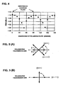
- FIG. 4 is a graph showing the polarization dependence of emission light of a surface-emitting type semiconductor laser in accordance with an embodiment of the present invention
- FIG. 5 shows diagrams for explaining the arrangement relation between a surface-emitting type semiconductor laser in accordance with an embodiment of the present invention and a reflection mirror;
- FIG. 6 is a view showing a variation example of the first optical module in accordance with an embodiment of the present invention.
- FIG. 7 is a view showing a second optical module in accordance with an embodiment of the present invention.
- FIG. 8 is a view showing optical transmission devices in accordance with an embodiment of the present invention.
- FIG. 1 is a view schematically showing a first optical module in accordance with an embodiment of the present invention.
- the optical module of the present embodiment includes a metal stem 5, and a vertical resonator type surface-emitting type semiconductor laser (a light emitting element in a broad sense: hereafter abbreviated as VCSEL) 10 electrically connected to the metal stem through a VCSEL submount (simply, a submount in a broad sense) 10a composed of ceramics and a metal film formed thereon (to secure insulation from the stem 5). Furthermore, a monitor PD (a photodetector in a broad sense) 20 for monitoring the amount of emission light of the VCSEL 10 is disposed on the stem 5.
- a monitor PD a photodetector in a broad sense
- the optical module of the present embodiment includes lead pins 1 - 3 for mutual transmission and reception of electrical signals with external devices; and by using them, the VCSEL 10, the VCSEL submount 10a and the monitor PD 20 are electrically connected by wire bonding.
- the VCSEL 10 As the VCSEL 10, one that can obtain linearly polarized light in two given polarization axes (first and second polarization axes in a broad sense) can be used. More specifically, the VCSEL 10 has a resonator structure in which a lower mirror (multilayer reflection film) layer 102, an active layer 104, and an upper mirror (multilayer reflection film) layer 106 formed with GaAs / AlGaAs type compound semiconductor materials are stacked in layers on an n-type GaAs substrate 100 in the (100) crystal plane, as shown in FIG. 2. It is noted that the reference numeral 108 denotes a dielectric layer composed of an oxide film. Also, reference numerals 112 and 114 in FIG.
- the VCSEL 10 has a current constricting layer 106a formed through oxidation of an internal part of an upper mirror layer 106.
- the density of an electrical current to be injected in the active layer 104 is controlled by the diameter of the current constricting layer 106a, such that the diameter of the active region 104a (emission region) is made to have a diameter suitable for the multimode oscillation (8 4 ⁇ m or more, for example).
- the diameter of the active layer 104 may be processed to a diameter with which a multimode oscillation is generated.
- the active layer 104 and the upper mirror layer 106 are formed in a circular configuration by anisotripic etching, to assume a circular resonator structure.
- the polarization characteristic of emission light depends on (is preferentially oriented in) the crystal orientation of the substrate. More specifically, when the (100) crystal plane is used, emission light has polarization predominant axes (in a broad sense, polarization axes) that can obtain strong linear polarization (a large amount of light) in mutually orthogonal two directions of the [011] and [0-11] axes.
- the polarization axes of the emission light are preferentially oriented in directions of the cleavage plane of the substrate (in a broad sense, in two specific crystal orientations).
- an emission aperture of the p-type electrode 112 that is formed on the resonator is formed to have isotropy, the density of an electric current injected into the resonator is uniformly distributed, such that the dependency of the polarization predominant axes of the VCSEL 10 on the direction of the cleavage plane of the substrate strengthens.
- the polarization predominant axes may not necessarily be perpendicular to each other.
- the resonator structure of the VCSEL is not limited to a circular shape, and the planar configuration of the resonator structure may be square (in a broad sense, rectangular), as shown in FIG. 3, for example.
- the planar configuration of the resonator structure may be square (in a broad sense, rectangular), as shown in FIG. 3, for example.
- FIG. 4 shows the relative intensity noise (RIN) of emission light of the VCSEL 10 when measured with 937.5 MHz as a noise characteristic, which is in a band used in a gigabit ISA network (GbE).
- the measurements were made with one of the cleavage plane directions of an n-type GaAs substrate 100 as a reference (0 degree).
- the noise is large in the cleavage plane directions, and it is confirmed that the noise decreases sharply at an intermediate angle between the two cleavage plane directions [011] and [0-11].
- the emission light of the VCSEL 10 has two polarization predominant axes which are preferentially oriented in the cleavage directions.
- a conventional photodetector element such as, a PN photo-diode, a PIN photo-diode, etc. which uses semiconductor such as Si, Ge, etc. or compound semiconductor (a GaAs type, InP type) can be used. More specifically, one having a photo-detecting wavelength band which suites the oscillation wavelength of the VCSEL 10 is used.
- the VCSEL 10, the VCSEL submount 10a and the monitor PD 20 described above are enclosed inside the metallic container 7 that is connected to (or formed in one piece with) the stem 5.
- the container 7 is disposed in a manner that a reflection mirror (in a broad sense, an optical member) 30 that has polarization selectivity as an emission window of the emission light of the VCSEL 10 and is provided above the VCSEL 10 and the monitor PD 20 intersects with a traveling direction of the emission light P1 of the VCSEL 10.
- the reflection mirror 30 has a reflection surface 30a in which a reflection film formed with a metal film (a single-layer or a multilayer) or a dielectric film (a single-layer or a multilayer) is formed on one surface (in a broader sense, a principal plane) of a glass plate.
- the reflection surface 30a has P-polarization whose transmittance is higher than that of S-polarization, and has a prescribed polarization transmission axis (in a broad sense, a third polarization axis).
- the transmittance of light in the reflection surface 30a is determined by the thickness, material, etc. of the reflection film, and depends on the number of layers.
- the reflection mirror 30 transmits a part of the emission light P1 of the VCSEL 10, and outputs the same as output light P2, and reflects the remaining of the light, and directs (injects) the same as monitor light P3 into the monitor PD.
- noise reduction of the optical module is achieved by giving a certain arrangement relation between the two polarization predominant axes of emission light of the VCSEL 10 and the polarization transmission axis of the reflection mirror 30. More specifically, the two polarization predominant axes of the VCSEL 10 along the substrate cleavage plane directions ([011] and [0-11]) are arranged so that neither of them overlaps with the polarization transmission axis of the reflection mirror 30. As a result, linearly polarized light of relatively low noise shown in FIG. 4 can be securely retrieved from the reflection mirror 30. Moreover, in view of the tolerance against fluctuations in the amount of output light and the amount of monitor light by a mode competition, as shown in FIG.
- an angle ⁇ 1 and an angle ⁇ 2 of the two polarization predominant axes of the VCSEL 10 defined with respect to the polarization transmission axis of the reflection mirror 30 may preferably be arranged to be equal to each other (for example, 45 degrees) (so that each can be at an intermediate position between the orthogonal cleavage plane directions of the substrate).
- FIG. 5 (B) when one of the two polarization predominant axes of the VCSEL 10 is arranged to match the polarization transmission axis of the reflection mirror 30, it is obvious from FIG. 4 that, when a mode competition occurs, the amount of output light of the optical module and the amount of monitor light to the monitor PD20 fluctuate greatly.
- the optical module of the present embodiment because the VCSEL 10 oscillates in a multimode, its emission light has low coherency, and degradation of the S/N ratio by the mode selection loss is few even when a multimode fiber is used. Moreover, the two polarization predominant axes of emission light of the VCSEL 10 are arranged so as not to overlap with the polarization transmission axis of the polarization plane 30a of the reflection mirror 30, such that, even when a mode competition occurs, fluctuations in the amount of light that passes the reflection mirror 30 and the amount of light that is reflected by the reflection mirror 30 are few. For this reason, the optical module of the present embodiment can realize a light source with low noise which is suitable for communication forms using multimode fibers.
- the light amount of output light P2 of the optical module and the light amount of monitor light P3 to the monitor PD20 can be stabilized according to the present embodiment.
- the polarized light in an axial direction located in the middle of the two polarization predominant axes has few fluctuations in the amount of light due to a mode competition, and therefore a light source with substantially reduced noise can be achieved.
- a diffraction grating (in a broad sense, an optical member) 32 may be used instead of using the reflection mirror 30, as shown in FIG. 6, as a variation example of the first optical module.
- the diffraction grating 32 is also disposed above the VCSEL 10 such that one of its planes (in a broad sense, a principal plane) 32a intersects with emission light P1 of the VCSEL 10.
- the arrangement of the diffraction grating 32 and the monitor PD 20 is decided so that a first order diffracted light (in a broad sense, a low-order diffracted light) is led to the monitor PD 20.
- the optical module of this variation example can provide linearly polarized light with low noise as output light P2, which is suitable for communication forms that use multimode fibers. Moreover, the tolerance against fluctuations in the light amount of output light P2 and monitor light P3 caused by a mode competition can be improved. Moreover, in accordance with the present embodiment, a composition to lead light to the monitor PD 20 by using optical diffraction may be adopted, besides the one using transmission, reflection or refraction.
- FIG. 7 is a view schematically showing a second optical module in accordance with a second embodiment of the present invention.
- This optical module is formed from a VCSEL 10 and an optical guide element of an optical waveguide type (in a broad sense, an optical member) 40.
- the VCSEL 10 can adopt the structure shown in, for example, FIG. 2 or FIG. 3, like the first optical module described above, and therefore its detailed description is omitted.
- the optical guide element 40 has an optical waveguide structure formed from a core 44 and a clad 42 that is composed of a material with a low refractive index than that of the core 44.
- a multimode fiber will be connected to a tip of the optical light guide element 40.
- the optical guide element 40 has a reflection surface (in a broad sense, a principle plane) 44a that is arranged to intersect with a traveling direction of emission light P1 of the VCSEL 10, and has a polarization reflection axis (in a broad sense, a polarization axis) with which S-polarization has a high reflecting power.
- emission light P1 of the VCSEL 10 is reflected by the reflection surface 44a and reflected light P2 is led to the core 44.
- an electrode section 46p for a p-type electrode and an electrode section 46n for an n-type electrode are provided, and, for example, the VCSEL 10 is flip-chip mounted with bumps 50 in a face down state. That is, this optical module receives electrical signals inputted from outside through the electrode sections 46p and 46n and operates.
- the core 44 and the clad 42 can be formed by using materials selected from the well-known materials used as materials for thin-film optical waveguides, silica glass optical fibers, plastic optical fibers, and the like, for example.
- silicon oxide SiO 2
- lithium niobate LiNbO 3
- silica glass optical fibers oxide glass represented by the above-mentioned silicon oxide, heavy metal fluoride glass (ZrF 4 -BaF 2 ), the chalcogenide glass (As-S, As-Ge-Se, Ge-S), and the like can be listed.
- materials used for plastic optical fibers polymethyl methacrylate (PMMA), epoxy resin, phenol resin, diallylphthalate, phenyl methacrylate, fluorine polymer, and the like can be listed.
- two polarization predominant axes along cleavage plane directions ([011], [0-11]) of the VCSEL 10 are disposed so as not to overlap the polarization reflection axis of the reflection surface 44a of the optical guide element 40.
- light P2 that passes the inside of the core 44 that composes the optical waveguide becomes linearly polarized light with low noise, and with few fluctuations in the amount of light due to a mode competition.
- the second optical module can also provide linearly polarized light with low noise as output light, which is suitable for communication forms that use multimode fibers, and the tolerance against fluctuations in the light amount of output light caused by a mode competition can be improved.
- FIG. 8 is a view showing optical transmission devices that use optical modules in accordance with an embodiment of the present invention.
- the optical transmission devices 90 mutually connect electronic devices 92, such as, a computer, display device, storage device, printer and the like.
- the electronic devices 92 may be information communication devices.
- the optical transmission device 90 may include a cable 94 and plugs 96 provided on both sides of the cable 94. More specifically, the cable 94 is a multimode fiber.
- the plug 96 is composed by including an optical module of the present embodiment as a light source for optical transmission. With the optical transmission devices, data can be transmitted among the electronic devices by optical signals.
- Electronic devices that are mutually connected by optical transmission devices of the present embodiment can include liquid crystal display monitors, digital CRTs (which may be used in the fields of finance, mail order, medical treatment, and education), liquid crystal projectors, plasma display panels (PDP), digital TVs, cash registers of retail stores (for POS), videos, tuners, gaming devices, and the like.
- liquid crystal display monitors digital CRTs (which may be used in the fields of finance, mail order, medical treatment, and education)
- liquid crystal projectors liquid crystal projectors
- plasma display panels (PDP) plasma display panels
- digital TVs digital TVs
- cash registers of retail stores for POS
- videos for tuners, gaming devices, and the like.
- the material that composes each layer of the VCSEL 10 is not limited to a GaAs material, but may be a compound semiconductor material of InP, GaN, or the like.
- the optical member is preferably a reflection mirror and a reflection surface of the reflection mirror preferably has a metal film or a dielectric film.
- the reflection surface preferably has P-polarization whose transmittance is higher than that of S-polarization.
- angles of the two polarization axes of emission light with respect to the polarization axis of the optical member are preferably 45 degrees.
- the optical member is preferably a diffraction grating and a low-order diffracted light is lead to the photo detector.
- the surface-emitting type semiconductor laser preferably comprises a substrate, a resonator structure formed on the substrate, the resonator structure having a lower mirror layer, an active layer and upper mirror, a mesa extending downward through the semiconductor layers at least to the active layer, and an upper electrode above the upper mirror wherein the mesa has a planar configuration which is a circle or square.
Landscapes
- Physics & Mathematics (AREA)
- Condensed Matter Physics & Semiconductors (AREA)
- General Physics & Mathematics (AREA)
- Electromagnetism (AREA)
- Optics & Photonics (AREA)
- Semiconductor Lasers (AREA)
- Optical Couplings Of Light Guides (AREA)
Applications Claiming Priority (2)
| Application Number | Priority Date | Filing Date | Title |
|---|---|---|---|
| JP2003315578 | 2003-09-08 | ||
| JP2003315578A JP2005085942A (ja) | 2003-09-08 | 2003-09-08 | 光モジュール、光伝送装置 |
Publications (2)
| Publication Number | Publication Date |
|---|---|
| EP1515406A2 true EP1515406A2 (de) | 2005-03-16 |
| EP1515406A3 EP1515406A3 (de) | 2005-11-23 |
Family
ID=34131936
Family Applications (1)
| Application Number | Title | Priority Date | Filing Date |
|---|---|---|---|
| EP04021236A Withdrawn EP1515406A3 (de) | 2003-09-08 | 2004-09-07 | Optisches Module und optische Übertragungsvorrichtung |
Country Status (4)
| Country | Link |
|---|---|
| US (1) | US7113658B2 (de) |
| EP (1) | EP1515406A3 (de) |
| JP (1) | JP2005085942A (de) |
| CN (1) | CN1595740A (de) |
Families Citing this family (38)
| Publication number | Priority date | Publication date | Assignee | Title |
|---|---|---|---|---|
| JP2007103576A (ja) * | 2005-10-03 | 2007-04-19 | Furukawa Electric Co Ltd:The | 面発光レーザモジュール |
| JP5080008B2 (ja) * | 2006-01-12 | 2012-11-21 | 株式会社リコー | 光源装置、光走査装置及びこれを用いる画像形成装置 |
| JP2010010155A (ja) * | 2008-06-24 | 2010-01-14 | Hitachi Ltd | 光モジュール |
| JP2010251649A (ja) | 2009-04-20 | 2010-11-04 | Hitachi Ltd | 面出射型レーザモジュールおよび面受光型モジュール |
| US9000466B1 (en) | 2010-08-23 | 2015-04-07 | Soraa, Inc. | Methods and devices for light extraction from a group III-nitride volumetric LED using surface and sidewall roughening |
| US8207554B2 (en) | 2009-09-11 | 2012-06-26 | Soraa, Inc. | System and method for LED packaging |
| US9293667B2 (en) | 2010-08-19 | 2016-03-22 | Soraa, Inc. | System and method for selected pump LEDs with multiple phosphors |
| US9293644B2 (en) | 2009-09-18 | 2016-03-22 | Soraa, Inc. | Power light emitting diode and method with uniform current density operation |
| US8933644B2 (en) | 2009-09-18 | 2015-01-13 | Soraa, Inc. | LED lamps with improved quality of light |
| US8269245B1 (en) * | 2009-10-30 | 2012-09-18 | Soraa, Inc. | Optical device with wavelength selective reflector |
| JP5522595B2 (ja) * | 2009-11-27 | 2014-06-18 | 株式会社リコー | 面発光レーザ素子、面発光レーザアレイ、光走査装置及び画像形成装置 |
| US10147850B1 (en) | 2010-02-03 | 2018-12-04 | Soraa, Inc. | System and method for providing color light sources in proximity to predetermined wavelength conversion structures |
| US8905588B2 (en) | 2010-02-03 | 2014-12-09 | Sorra, Inc. | System and method for providing color light sources in proximity to predetermined wavelength conversion structures |
| US20110186874A1 (en) * | 2010-02-03 | 2011-08-04 | Soraa, Inc. | White Light Apparatus and Method |
| DE102010003034A1 (de) | 2010-03-18 | 2011-09-22 | Vertilas Gmbh | Leuchteinheit |
| US8541951B1 (en) | 2010-11-17 | 2013-09-24 | Soraa, Inc. | High temperature LED system using an AC power source |
| US8896235B1 (en) | 2010-11-17 | 2014-11-25 | Soraa, Inc. | High temperature LED system using an AC power source |
| USD720310S1 (en) | 2011-06-17 | 2014-12-30 | Soraa, Inc. | Triangular semiconductor die |
| JP5853473B2 (ja) * | 2011-08-03 | 2016-02-09 | 株式会社リコー | 光走査装置及び画像形成装置 |
| US9488324B2 (en) | 2011-09-02 | 2016-11-08 | Soraa, Inc. | Accessories for LED lamp systems |
| JP6016189B2 (ja) * | 2011-09-08 | 2016-10-26 | 株式会社リコー | パッケージ部材及び光デバイス |
| US8985794B1 (en) | 2012-04-17 | 2015-03-24 | Soraa, Inc. | Providing remote blue phosphors in an LED lamp |
| US9978904B2 (en) | 2012-10-16 | 2018-05-22 | Soraa, Inc. | Indium gallium nitride light emitting devices |
| US9761763B2 (en) | 2012-12-21 | 2017-09-12 | Soraa, Inc. | Dense-luminescent-materials-coated violet LEDs |
| JP2014135307A (ja) * | 2013-01-08 | 2014-07-24 | Ricoh Co Ltd | 光デバイス、光走査装置及び画像形成装置 |
| US8994033B2 (en) | 2013-07-09 | 2015-03-31 | Soraa, Inc. | Contacts for an n-type gallium and nitrogen substrate for optical devices |
| US9410664B2 (en) | 2013-08-29 | 2016-08-09 | Soraa, Inc. | Circadian friendly LED light source |
| DE102013220787A1 (de) * | 2013-10-15 | 2015-04-16 | Robert Bosch Gmbh | Mikromechanisches Bauelement mit integrierter Photodiode und Mikroprojektor |
| US9419189B1 (en) | 2013-11-04 | 2016-08-16 | Soraa, Inc. | Small LED source with high brightness and high efficiency |
| JP6717621B2 (ja) * | 2015-11-13 | 2020-07-01 | ローム株式会社 | 光学装置および光学装置の製造方法 |
| DE102016104947A1 (de) * | 2016-03-17 | 2017-09-21 | Osram Opto Semiconductors Gmbh | Optoelektronisches Bauelement und Verfahren zum Betreiben eines optoelektronischen Bauelements |
| WO2018043763A1 (en) * | 2016-09-02 | 2018-03-08 | Kyushu University, National University Corporation | Continuous-wave organic thin-film distributed feedback laser and electrically driven organic semiconductor laser diode |
| KR102567101B1 (ko) | 2017-02-07 | 2023-08-16 | 고쿠리쓰다이가쿠호진 규슈다이가쿠 | 전류주입형 유기 반도체 레이저 다이오드, 그 제조 방법 및 프로그램 |
| WO2020126936A1 (en) | 2018-12-17 | 2020-06-25 | Ams International Ag | Light emitting module including enhanced eye-safety feature |
| US10985531B2 (en) * | 2019-01-27 | 2021-04-20 | Hewlett Packard Enterprise Development Lp | Intensity noise mitigation for vertical-cavity surface emitting lasers |
| JP7810330B2 (ja) * | 2022-05-17 | 2026-02-03 | 古河ファイテルオプティカルコンポーネンツ株式会社 | 光半導体装置 |
| JPWO2024142624A1 (de) * | 2022-12-26 | 2024-07-04 | ||
| WO2025219397A1 (en) * | 2024-04-17 | 2025-10-23 | Quside Technologies S.L. | A device comprising a lasing component for emitting laser light |
Family Cites Families (15)
| Publication number | Priority date | Publication date | Assignee | Title |
|---|---|---|---|---|
| JPH04121771A (ja) | 1990-09-12 | 1992-04-22 | Ricoh Co Ltd | クリーニング装置 |
| JP2555317Y2 (ja) * | 1991-04-19 | 1997-11-19 | 三洋電機株式会社 | 面発光レーザ装置 |
| JPH06138413A (ja) * | 1992-10-29 | 1994-05-20 | Canon Inc | プレート型偏光分離装置及び該偏光分離装置を用いた偏光照明装置 |
| US5359447A (en) | 1993-06-25 | 1994-10-25 | Hewlett-Packard Company | Optical communication with vertical-cavity surface-emitting laser operating in multiple transverse modes |
| KR100258927B1 (ko) * | 1996-10-29 | 2000-06-15 | 윤종용 | 다중 트랙 스캔 가능한 호환형 광픽업장치 |
| US6327037B1 (en) * | 1997-11-12 | 2001-12-04 | Chien Chou | Optical rotation angle polarimeter |
| US6069905A (en) | 1997-12-31 | 2000-05-30 | Honeywell Inc. | Vertical cavity surface emitting laser having intensity control |
| JP2000081524A (ja) | 1998-09-07 | 2000-03-21 | Sony Corp | 光送受信システム |
| GB2349740A (en) | 1999-05-05 | 2000-11-08 | Mitel Semiconductor Ab | Vertical cavity surface emitting laser with monitoring diode |
| EP1182436A1 (de) * | 2000-01-31 | 2002-02-27 | Mitsubishi Denki Kabushiki Kaisha | WELLENLäNGENMONITOR, VERFAHREN ZU SEINER JUSTIERUNG, STABILISIERTE LICHTQUELLE UND KOMMUNIKATIONSSYSTEM UNTER VERWENDUNG VON STABILISIERTEN LICHTQUELLEN |
| US6963598B1 (en) | 2000-05-23 | 2005-11-08 | Finisar Corporation | System and method for VCSEL polarization control |
| US6687268B2 (en) | 2001-03-26 | 2004-02-03 | Seiko Epson Corporation | Surface emitting laser and photodiode, manufacturing method therefor, and optoelectric integrated circuit using the surface emitting laser and the photodiode |
| JP2002368334A (ja) | 2001-03-26 | 2002-12-20 | Seiko Epson Corp | 面発光レーザ、フォトダイオード、それらの製造方法及びそれらを用いた光電気混載回路 |
| US6931187B2 (en) * | 2002-12-11 | 2005-08-16 | Kwangju Institute Of Science And Technology | Mode-filtering and mode-selecting method in multi-mode waveguide, and waveguide amplifier, semiconductor laser, and VCSEL using the method |
| US6859330B2 (en) * | 2003-06-04 | 2005-02-22 | Intel Corporation | Micromachined pellicle splitters and tunable laser modules incorporating same |
-
2003
- 2003-09-08 JP JP2003315578A patent/JP2005085942A/ja active Pending
-
2004
- 2004-09-07 US US10/934,381 patent/US7113658B2/en not_active Expired - Lifetime
- 2004-09-07 CN CNA2004100745896A patent/CN1595740A/zh active Pending
- 2004-09-07 EP EP04021236A patent/EP1515406A3/de not_active Withdrawn
Also Published As
| Publication number | Publication date |
|---|---|
| US20050084218A1 (en) | 2005-04-21 |
| CN1595740A (zh) | 2005-03-16 |
| US7113658B2 (en) | 2006-09-26 |
| JP2005085942A (ja) | 2005-03-31 |
| EP1515406A3 (de) | 2005-11-23 |
Similar Documents
| Publication | Publication Date | Title |
|---|---|---|
| US7113658B2 (en) | Optical module, and optical transmission device | |
| EP2866067B1 (de) | Gitterbasierter optischer Koppler | |
| US7627018B1 (en) | Polarization control using diffraction gratings in VCSEL waveguide grating couplers | |
| EP1610426B1 (de) | Optisches halbleiterbauelement und integrierte optische halbleiterschaltung | |
| US5995692A (en) | Light emitting device module | |
| US9042690B2 (en) | Hybrid laser light sources for photonic integrated circuits | |
| US20200067276A1 (en) | External cavity laser | |
| JP2624279B2 (ja) | スラブ導波光出射半導体レーザー | |
| JP4634010B2 (ja) | 半導体光素子 | |
| JP2004356629A (ja) | 面屈折入射型受光素子及びその製造方法 | |
| CA2017732A1 (en) | Method for reducing facet reflectivities of semiconductor light sources and device thereof | |
| EP0150214B1 (de) | Laser mit gekoppelten resonatoren | |
| US4297651A (en) | Methods for simultaneous suppression of laser pulsations and continuous monitoring of output power | |
| JP2005086067A (ja) | 光モジュール、光伝送装置 | |
| JP6019522B2 (ja) | 面発光レーザ装置 | |
| JP2000208869A (ja) | 発光素子モジュ―ル | |
| JP6210548B2 (ja) | 面発光レーザ素子、レーザ素子アレイ、光源および光モジュール | |
| CN108169931B (zh) | 一种片上可调谐多模干涉反射镜 | |
| JPH1117286A (ja) | 波長可変レーザ装置 | |
| US7532379B2 (en) | Optical modulator with side access | |
| US20030103761A1 (en) | Folded light path for planar optical devices | |
| JP5374196B2 (ja) | 半導体光素子 | |
| US20250125584A1 (en) | Distributed feedback lasers with tunable distributed bragg reflector integration | |
| CA1118085A (en) | Methods for simultaneous suppression of laser pulsations and continuous monitoring of output power | |
| JP2665024B2 (ja) | 半導体レーザ |
Legal Events
| Date | Code | Title | Description |
|---|---|---|---|
| PUAI | Public reference made under article 153(3) epc to a published international application that has entered the european phase |
Free format text: ORIGINAL CODE: 0009012 |
|
| AK | Designated contracting states |
Kind code of ref document: A2 Designated state(s): AT BE BG CH CY CZ DE DK EE ES FI FR GB GR HU IE IT LI LU MC NL PL PT RO SE SI SK TR |
|
| AX | Request for extension of the european patent |
Extension state: AL HR LT LV MK |
|
| PUAL | Search report despatched |
Free format text: ORIGINAL CODE: 0009013 |
|
| AK | Designated contracting states |
Kind code of ref document: A3 Designated state(s): AT BE BG CH CY CZ DE DK EE ES FI FR GB GR HU IE IT LI LU MC NL PL PT RO SE SI SK TR |
|
| AX | Request for extension of the european patent |
Extension state: AL HR LT LV MK |
|
| 17P | Request for examination filed |
Effective date: 20051229 |
|
| AKX | Designation fees paid |
Designated state(s): DE GB |
|
| STAA | Information on the status of an ep patent application or granted ep patent |
Free format text: STATUS: THE APPLICATION IS DEEMED TO BE WITHDRAWN |
|
| 18D | Application deemed to be withdrawn |
Effective date: 20060606 |