EP1511331A1 - Steuerung zum umschalten eines wellenlängen-gemultiplexten optischen signals - Google Patents
Steuerung zum umschalten eines wellenlängen-gemultiplexten optischen signals Download PDFInfo
- Publication number
- EP1511331A1 EP1511331A1 EP02733354A EP02733354A EP1511331A1 EP 1511331 A1 EP1511331 A1 EP 1511331A1 EP 02733354 A EP02733354 A EP 02733354A EP 02733354 A EP02733354 A EP 02733354A EP 1511331 A1 EP1511331 A1 EP 1511331A1
- Authority
- EP
- European Patent Office
- Prior art keywords
- switching
- optical
- signal
- information
- wavelength
- Prior art date
- Legal status (The legal status is an assumption and is not a legal conclusion. Google has not performed a legal analysis and makes no representation as to the accuracy of the status listed.)
- Granted
Links
Images


Classifications
-
- H—ELECTRICITY
- H04—ELECTRIC COMMUNICATION TECHNIQUE
- H04J—MULTIPLEX COMMUNICATION
- H04J14/00—Optical multiplex systems
- H04J14/02—Wavelength-division multiplex systems
- H04J14/0201—Add-and-drop multiplexing
- H04J14/0202—Arrangements therefor
- H04J14/021—Reconfigurable arrangements, e.g. reconfigurable optical add/drop multiplexers [ROADM] or tunable optical add/drop multiplexers [TOADM]
- H04J14/0212—Reconfigurable arrangements, e.g. reconfigurable optical add/drop multiplexers [ROADM] or tunable optical add/drop multiplexers [TOADM] using optical switches or wavelength selective switches [WSS]
-
- H—ELECTRICITY
- H04—ELECTRIC COMMUNICATION TECHNIQUE
- H04J—MULTIPLEX COMMUNICATION
- H04J14/00—Optical multiplex systems
- H04J14/02—Wavelength-division multiplex systems
- H04J14/0227—Operation, administration, maintenance or provisioning [OAMP] of WDM networks, e.g. media access, routing or wavelength allocation
- H04J14/0241—Wavelength allocation for communications one-to-one, e.g. unicasting wavelengths
-
- H—ELECTRICITY
- H04—ELECTRIC COMMUNICATION TECHNIQUE
- H04Q—SELECTING
- H04Q11/00—Selecting arrangements for multiplex systems
- H04Q11/0001—Selecting arrangements for multiplex systems using optical switching
- H04Q11/0005—Switch and router aspects
-
- H—ELECTRICITY
- H04—ELECTRIC COMMUNICATION TECHNIQUE
- H04J—MULTIPLEX COMMUNICATION
- H04J14/00—Optical multiplex systems
- H04J14/02—Wavelength-division multiplex systems
- H04J14/0227—Operation, administration, maintenance or provisioning [OAMP] of WDM networks, e.g. media access, routing or wavelength allocation
-
- H—ELECTRICITY
- H04—ELECTRIC COMMUNICATION TECHNIQUE
- H04J—MULTIPLEX COMMUNICATION
- H04J14/00—Optical multiplex systems
- H04J14/02—Wavelength-division multiplex systems
- H04J14/0278—WDM optical network architectures
- H04J14/0279—WDM point-to-point architectures
-
- H—ELECTRICITY
- H04—ELECTRIC COMMUNICATION TECHNIQUE
- H04J—MULTIPLEX COMMUNICATION
- H04J14/00—Optical multiplex systems
- H04J14/02—Wavelength-division multiplex systems
- H04J14/0278—WDM optical network architectures
- H04J14/0283—WDM ring architectures
-
- H—ELECTRICITY
- H04—ELECTRIC COMMUNICATION TECHNIQUE
- H04J—MULTIPLEX COMMUNICATION
- H04J14/00—Optical multiplex systems
- H04J14/02—Wavelength-division multiplex systems
- H04J14/0287—Protection in WDM systems
- H04J14/0289—Optical multiplex section protection
- H04J14/0291—Shared protection at the optical multiplex section (1:1, n:m)
-
- H—ELECTRICITY
- H04—ELECTRIC COMMUNICATION TECHNIQUE
- H04Q—SELECTING
- H04Q11/00—Selecting arrangements for multiplex systems
- H04Q11/0001—Selecting arrangements for multiplex systems using optical switching
- H04Q11/0005—Switch and router aspects
- H04Q2011/0037—Operation
- H04Q2011/0039—Electrical control
-
- H—ELECTRICITY
- H04—ELECTRIC COMMUNICATION TECHNIQUE
- H04Q—SELECTING
- H04Q11/00—Selecting arrangements for multiplex systems
- H04Q11/0001—Selecting arrangements for multiplex systems using optical switching
- H04Q11/0062—Network aspects
- H04Q2011/0069—Network aspects using dedicated optical channels
-
- H—ELECTRICITY
- H04—ELECTRIC COMMUNICATION TECHNIQUE
- H04Q—SELECTING
- H04Q11/00—Selecting arrangements for multiplex systems
- H04Q11/0001—Selecting arrangements for multiplex systems using optical switching
- H04Q11/0062—Network aspects
- H04Q2011/0077—Labelling aspects, e.g. multiprotocol label switching [MPLS], G-MPLS, MPAS
-
- H—ELECTRICITY
- H04—ELECTRIC COMMUNICATION TECHNIQUE
- H04Q—SELECTING
- H04Q11/00—Selecting arrangements for multiplex systems
- H04Q11/0001—Selecting arrangements for multiplex systems using optical switching
- H04Q11/0062—Network aspects
- H04Q2011/0088—Signalling aspects
Definitions
- the present invention relates to a wavelength-division multiplexing (WDM) communication system.
- WDM wavelength-division multiplexing
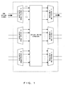
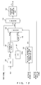
- Fig. 1 shows the basic configuration of a conventional optical cross-connect.
- a wavelength demultiplexer 10 demultiplexes the optical signal into a plurality of optical signals each with one of wavelengths ⁇ 1 through ⁇ n.
- the demultiplexed optical signals are inputted to an optical switch structure after being demultiplexed.
- the optical signal is outputted for each wavelength again and is inputted to a wavelength multiplexer 11.
- the wavelength multiplexer 11 applies wavelength-division multiplexing (WDM) to the optical signals with each wavelength, and generates/outputs a WDM optical signal.
- WDM wavelength-division multiplexing
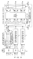
- Fig. 2 shows a conventional WDM system.
- an optical supervisory channel (OSC) control signal is provided separately from a WDM optical signal, and the OSC control signal stores information for switching light with each wavelength.
- OSC optical supervisory channel
- each optical cross-connect station determines the switching direction of optical switching, based on the contents of the OSC signal and performs the optical switching.
- optical switching information must be put on the OSC control signal, the trace information of SONET/SDH device or the like for outputting each wavelength must be transferred to an OSC signal transmitting unit provided for a WDM device. Therefore, such information must be transmitted /received between all SONET/SDH devices 15 or transponder devices 16 (a device for converting received light into light with a predetermined wavelength in order to apply WDM to it to transmit it), connected to the WDM device.
- control information stored in the header of data formed in a frame is once demultiplexed for each frame without any conversion by the photo-coupler 18 of the WDM station (WDM device) 17, is terminated at a data communication channel (DCC) termination/OSC transmission unit 19 and is converted into an electrical signal. Then, necessary control information is extracted from the electrical signal and is converted into an optical signal with an OSC channel wavelength.
- This OSC channel optical signal is multiplexed onto a main signal transmitted from a WDM device 20 in the latter stage of the WDM device 20 for multiplexing optical signals from the SONET/SDH device 15 or the like, by a coupler 21.
- the WDM optical signal generated thus is transmitted through a transmission line and is inputted to an optical cross-connect station 25.
- the optical cross-connect station 25 demultiplexes an OSC channel from the received WDM optical signal in an OSC separation unit 22, and converts the OSC optical signal into an electrical signal in an OSC termination/transmission unit 23.
- the OSC termination/transmission unit 23 extracts control information from the electrical signal and issues a switching instruction to an optical switch structure 12. Then, this control information is converted into an optical signal again and is inputted to an OSC insertion unit 24 as an OSC optical signal.
- the WDM optical signal from which the OSC signal is separated is demultiplexed into signals with each wavelength by a wavelength demultiplexer 10, and is switched by the optical switch structure 12. Then, after WDM is applied to the demultiplexed signals in a wavelength multiplexing unit 11, the OSC signal is inserted in the multiplexed signal by the OSC insertion unit 24 and is transmitted from the optical cross-connect station 25.
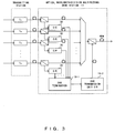
- Fig. 3 explains the conventional problems.
- a communication device such as a SONET/SDH device or the like provided for each channel is installed in the same station as the WDM device as a separate communication means, there is no need for optical/electrical conversion, since electrical signals can be used. Therefore, a simple and inexpensive communication method for transmitting/receiving such information can be realized.
- a communication device such as a SONET/SDH device or the like is not installed in the same station as the WDM device, communication must be conducted by light as long as connection is made only by an optical fiber. In that case, cost increases.
- the switching control method of the present invention performs the switching control of an optical-connect device, and comprises a control information transmitting step of suspending the transmission of a main signal and transmitting control information for instructing the switching control of the optical cross-connect device utilizing the wavelength of the main signal, a completion notice step of transmitting a signal for indicating the completion of switching information, utilizing the main signal wavelength after transmitting the control information and a re-start step of re-starting the transmission of a main signal suspended, when receiving a switching completion notice.
- the control device of the present invention performs the switching control of an optical cross-connect, and comprises a control information transmitting unit for suspending the transmission of a main signal and transmitting control information for instructing the switching control of the optical cross-connect device utilizing the wavelength of a main signal, a completion notification unit for transmitting a signal for indicating the completion of switching, utilizing a main signal wavelength after transmitting the control information and a re-start unit for re-starting the transmission of a main signal suspended, when receiving a switching completion notice.
- the optical cross-connect device of the present invention comprises an optical switch for switching an optical communication line, a control information receiving unit for receiving switching information transmitted utilizing the wavelength of a main signal, a switching control unit for instructing the optical switch to switch the optical communication line, according to the control information after receiving a switching information end signal and a completion notification unit for notifying the transmitting source of switching information for the completion of the switching.
- the configuration to extract switching information from converted electrical signal from optical signals for each wavelength, put it in the optical supervisory control channel and send it in order to put the switching information in the wavelength signal of the optical supervisory control channel is not needed.
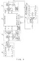
- Fig. 4 shows the entire configuration of a system according to the preferred embodiment of the present invention.
- a SONET/SDH device 100 accommodating a plurality of transmitters Tx including a transponder and the like is provided to transmit optical signals with each wavelength.
- the optical signals with each wavelength are multiplexed by an optical multiplexing device 101.
- the optical multiplexing device 101 comprises an optical multiplexer and an optical amplifier.
- Each optical signal transmitted from the optical multiplexing device 101 is transmitted through a transmission line as a WDM optical signal and is inputted to the wavelength multiplexing device 102 of the optical cross-connect device.
- a photo-coupler is provided before the optical demultiplexer of the wavelength demultiplexing device 102, and routing information and the like is extracted from the WDM optical signal.
- the extracted optical signal including routing information and the like is converted into an electrical signal by a photo-diode, which is an optical/electrical conversion device, and is amplified by a pre-amplifier. Then, the electrical signal is processed by a circuit shown in Fig. 6, and switching information is transferred to an optical switch (SW) structure 103.
- the optical SW structure 103 switches an optical route, according to the switching information. Thus, a specific optical signal is outputted from a drop port 110, and another optical signal is inputted from an add port 111. After switching these optical signals, the optical SW structure 103 outputs optical signals to the optical multiplexer of the optical multiplexing device 104.
- the optical SW structure 103 also outputs switching information.
- the optical multiplexer applies WDM to optical signals to generate a WDM optical signal.
- the WDM optical signal is amplified by an optical amplifier. Then, switching information converted from an electrical signal to an optical signal by a photo-coupler is multiplexed and is transmitted to a transmission line.
- the optical multiplexing device 105 amplifies a received optical signal by an optical amplifier, demultiplexes the amplified optical signal into optical signals with each wavelength by an optical demultiplexer and transfers the signals to the receiving device Rx of the SONET/SDH device station 106.
- the switching time of a currently known practical optical switch is expressed in units of milli-seconds. This means that information that is modulated in units of Gbps and is accommodated in each wavelength channel cannot be switched without instantaneous interruption. If the system includes an optical amplifier, an instantaneous interruption time accompanying the switching of an optical switch becomes longer and amounts to 30 through 100ms. After all, in order to switch an optical switch without instantaneous interruption, a technology for switching at an electrical level without instantaneous interruption must be applied. For such a reason, when an optical switch is switched by transmitting optical switching information to an optical switching station disposed in a WDM network system, the instantaneous interruption of the wavelength channel always occurs.
- the output of the wavelength signal must be reduced to a proper level while the switching is being performed. Even when there is no possibility that an optical surge may occur, the instantaneous interruption of light cannot be avoided at the time of switching. Therefore, even when the transmitting side transmits an optical signal at the time of switching, the receiving side cannot receive information. In other words, if the transmitting side suspends the transmission of optical signals when performing switching, there are no problems. Therefore, the transmitter of a channel to be switched or the transmitter of an optical signal with a specific wavelength of a WDM optical signal can also be used to transmit information for light switching besides communication information to be essentially transmitted.
- a signal composing switching information must be composed of a bit rate far lower than that of a main signal, such as approximately 1.5Mbps. Then, since the WDM main signal is modulated at high speed and hardly includes low-speed signal components, switching information can be accurately extracted as long as the characteristic of a switching information receiving unit provided for an optical cross-connect station or a receiving side device is optimized for this low-speed bit rate.
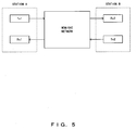
- FIG. 5 conceptually shows that stations A and B are connected by a WDM/OXC (optical cross-connect) network.
- Station A is provided with a transmitter Tx1 and a receiver Rx1.
- Station B is provided with a transmitter Tx2 and a receiver Rx2.
- Optical signals are transmitted/received between the transmitter Tx1 and the receiver Rx2 or between the transmitter Tx2 and the receiver Rx1.
- Fig. 6 shows the output signal pattern of a transmitter (Tx1).
- Fig. 7 shows switching sequence according to the preferred embodiment of the present invention.
- a transmitter suspends the transmission of usually transmitted signals on a wavelength for switching and intentionally causes output interruption. Then, the transmitter transmits switching information, which is a low-speed modulation signal, using the wavelength, that is, the channel. Then, after the transmission of switching information is completed, the transmitter transmits a fixed pattern signal with a prescribed pattern and starts switching. Then, after receiving a switching completion notice, the transmitter re-starts transmitting usually transmitted signals.
- switching information which is a low-speed modulation signal
- Fig. 8 shows another example of the switching sequence according to the preferred embodiment of the present invention.
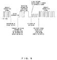
- Fig. 9 shows another fixed signal pattern outputted by the transmitter.
- Fig. 9 Although the fixed pattern of Fig. 9 is almost the same as that of Fig. 6, in Fig. 9, its output is reduced lower than that of a usual signal. Switching is performed while transmitting a fixed pattern. However, when performing switching, a fixed pattern suddenly appears in a new route. As described above, this causes a surge to lead to a possibility of damaging an optical amplifier or the like. Therefore, the output of a fixed pattern is reduced to a level such that such a surge may not damage an optical amplifier or the like.
- switching information to an optical cross-connect device can be received by only one monitor for each WDM line provided for an optical switching station.
- a receiver for receiving each segment of switching information for each wavelength group can be provided. Since such a method does not require a means for demultiplexing an optical signal in a WDM state into each channel, device configuration can be simplified. Therefore, device size can be reduced and also cost can be suppressed, which is an advantage. Specifically, low-speed switching information is put on a wavelength for switching and high-speed information is put on other wavelengths.
- the circuit can detect only low-speed switching information. Since this fact applies to a signal with any wavelength, by detecting a WDM optical signal by a low-speed circuit, switching information can be extracted without demultiplexing a signal with a specific wavelength.
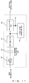
- Fig. 10 shows the respective configurations of a transmitter and receiver according to the preferred embodiment of the present invention.
- the transmitter comprises a termination LSI 120 for receiving/terminating transmission data and converting the data into electrical signals, a circuit 121 which is described later with reference to Figs. 12 or 15, and an electrical/óptical conversion unit 122.
- the receiver When an optical signal arrives, the receiver receives the optical signal by an optical/electrical conversion unit 125 and converts the optical signal into an electrical signal.
- a pre-amplifier 126 amplifies electrical signals obtained by converting received optical signals to be powered so as to be suitable for a later process.
- the output of the pre-amplifier 126 is supplied to a switching information extraction unit 123, an optical interruption detection unit 124, an equalizing filter 127 and a timing clock extraction unit 128.
- the timing clock extraction unit 128 generates timing signals for extracting data from received signals.
- the equalizing filter 127 re-shapes signal waveforms to waveforms suitable for data extraction by eliminating the RF components of received signals or the like.
- the output of the equalizing filter 127 is inputted to a data extraction unit 129, and extracts data, according to a timing clock from the timing clock extraction unit 128.
- the extracted data is outputted through the termination LSI 130 as transmission data.
- the switching information extraction unit 123 has a configuration shown in Fig. 11. The details are not presented here, but the operation is as follows.
- the switching information extraction unit 123 extracts switching information and inputs the switching information to the block 121 of the transmitter. Simultaneously, the switching information extraction unit 123 notifies a higher layer of the switching information.
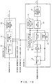
- Fig. 11 shows one configuration of the switching information extraction circuit shown in Fig. 10.
- the circuit shown in Fig. 11 receives a signal from the pre-amplifier 126 shown in Fig. 10. This signal is transmitted through a low-band pass filter 140. Thus, high-speed information signals other than a low-speed switching information signal are eliminated. Furthermore, a DC component elimination unit eliminates DC components. Then, the switching information is amplified by a post-amplifier 142, and is supplied to a data detection unit 143 and a timing clock extraction unit 144. The timing clock extraction unit 144 extracts a timing clock needed to detect data and supplies the timing clock to the data detection unit 143. Simultaneously, the timing clock extraction unit 144 is used as a clock signal. The data detection unit 143 detects data from the signal from the post-amplifier 142, based on the timing clock from the timing clock extraction unit 144, and outputs the result as switching information.
- switching information is composed of a low bit rate, it is generally known that if data, "0" or "1", is consecutively inputted to a receiver, transmission quality degrades.
- the signal string of switching information is prevented from becoming the continuation of "0" or "1" for the purpose of preventing the above problem.
- Fig. 12 shows one configuration of the block 121 shown in Fig. 10.
- Fig. 13 shows examples of the data or clocks of each line in the circuit shown in Fig. 12.
- a clock CLK synchronous with a main signal to be used in the transmitter is divided by N (CLKn) by a frequency divider 150 and is branched into two groups. One group is further divided by M (CLKm), and is used to generate a frame (DTS) including switching information in a switching information transmitting frame generation unit 153.
- the other group of CLKn is converted into a pulse string PLS0 by a differential circuit 151, and a pulse string PLS1 is obtained by inverting this PLS0 by an inversion circuit 154. Then, both PLS0 and PLS1 are inputted to a selector 155. Then, if the DTS is "1”, PLS0 is superimposed on the DTS to generate a DTS' . If the DTS is "0", PLS1 is superimposed on the DTS to generate a DTS'.
- a selector 156 it is determined whether to transmit usual main signal data or an optical cross-connect switching control signal DTS', according to the instruction of a switching information insertion signal from a higher layer, and is optically outputted by an electrical/optical conversion unit 157.
- a CLK shown in Fig. 13(a) is a basic clock signal, and CLKn is obtained by dividing the CLK by N.
- PLS0 and PLS1 are the differential signal of the CLKn and its inverted signal, respectively.
- the frame bits of the DTS are generated according to clock CLKm.
- each of PLS0 and PLS1, which are high-speed clocks generated from CLKn becomes a signal which becomes "1" or "0" at specific intervals. If the bit of the DTS is "H”, PLS1 is superimposed on the DTS. If the bit is "L”, PLS0 is superimposed on the DTS. Therefore, DTS' on which PLS0 or PLS1 is superimposed, changes from “H” to "L” or from "L” to "H” at specific intervals.
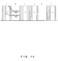
- Fig. 14 shows one structure of a signal for suppressing a non-linear effect, according to the preferred embodiment of the present invention.
- each bit of switching information is expressed by a fine consecutive pulse and the bad influence on other wavelengths of the non-linear optical effect is suppressed. Therefore, although the speed of the fine consecutive pulse is approximately 1Gbps, the speed of a signal expressed by these envelopes becomes approximately 1.5Mbps. The signal of this around 1.5Mbps is detected as the switching information.
- Fig. 15 shows the configuration of a circuit provided for a transmitter, for suppressing the respective influences of the degradation of transmission quality due to the continuation of "1" or "0" and that due to a non-linear optical effect.
- Fig. 16 shows examples of the data or clock of each line in the circuit shown in Fig. 15.
- the circuit shown in Fig. 15 superimposes a bit string obtained by dividing the CLK synchronous with a main signal by L using the frequency demultiplexer 160 on a switching signal to generate a DTS' in the selector 155 shown in Fig. 12 only when the switching signal is "1".
- the number of L is made low such as 2 or 3.
- the frequency of PLS1 is higher than that of PLS0.
- the DTS' can be made "H” in a fairly low frequency.
- the DTS is "H"
- a non-linear effect easily occurs since optical power is transmitted through an optical transmission line. Therefore, an operation for dropping the DTS to "L” is performed more frequently.
- a frequency used to invert the data value of a DTS' differs between when the data value is "H” and when it is "L".
- Fig. 17 shows one structure of a switching information frame.
- one receiver receives switching information. Therefore, if a plurality of wavelengths simultaneously transmits switching information, such a case cannot be coped with.
- Such a problem can be solved as follows.
- the "error detection/correction" section of the format is detected to be abnormal if a transmitter with a plurality of wavelength channels transmits switching information.
- the collision of switch requests is detected and switching is adjusted.
- the receiver computes the transmitted data and matches the data with an error detection/correction code.
- Fig. 18 explains a switching process of matching a pair of routes in opposed nodes.
- the output of a transmitter Tx1 is transmitted through a route of OXC1 ⁇ OXC2 and is received by a receiver Rx2, whereas a signal outputted from a transmitter Tx2 for the other pair is transmitted through the same route conversely OXC2 ⁇ OXC1 and is received by a receiver Rx1.
- the initial route is redundantly switched to a route of OXC1 ⁇ OVC2 ⁇ OXC3.
- optical cross-connect has been described as one component, the same description also applies to an optical router as one component.
- the switching of an optical switching station can be freely performed from any station, and accordingly, switching can be performed at low cost.
Landscapes
- Engineering & Computer Science (AREA)
- Computer Networks & Wireless Communication (AREA)
- Signal Processing (AREA)
- Optical Communication System (AREA)
- Use Of Switch Circuits For Exchanges And Methods Of Control Of Multiplex Exchanges (AREA)
- Time-Division Multiplex Systems (AREA)
Applications Claiming Priority (1)
| Application Number | Priority Date | Filing Date | Title |
|---|---|---|---|
| PCT/JP2002/005611 WO2003105496A1 (ja) | 2002-06-06 | 2002-06-06 | 波長分割多重光信号の切り替え制御装置 |
Publications (3)
| Publication Number | Publication Date |
|---|---|
| EP1511331A1 true EP1511331A1 (de) | 2005-03-02 |
| EP1511331A4 EP1511331A4 (de) | 2011-05-11 |
| EP1511331B1 EP1511331B1 (de) | 2012-07-04 |
Family
ID=29727321
Family Applications (1)
| Application Number | Title | Priority Date | Filing Date |
|---|---|---|---|
| EP02733354A Expired - Lifetime EP1511331B1 (de) | 2002-06-06 | 2002-06-06 | Steuerung zum umschalten eines wellenlängen-gemultiplexten optischen signals |
Country Status (4)
| Country | Link |
|---|---|
| US (1) | US7313327B2 (de) |
| EP (1) | EP1511331B1 (de) |
| JP (1) | JP3910615B2 (de) |
| WO (1) | WO2003105496A1 (de) |
Families Citing this family (5)
| Publication number | Priority date | Publication date | Assignee | Title |
|---|---|---|---|---|
| WO2004051897A1 (ja) * | 2002-11-29 | 2004-06-17 | Fujitsu Limited | パケット伝送システム及び端局装置 |
| WO2006072406A1 (de) * | 2004-12-30 | 2006-07-13 | Nokia Siemens Networks Gmbh & Co. Kg | Verfahren zur übertragung von datenpaketen mittels eines optischen burst-switching-netzwerks und netzknoten für ein optisches burst-switching-netzwerk |
| US7706685B2 (en) * | 2005-09-20 | 2010-04-27 | Lockheed Martin Corporation | Data communication network using optical power averaged multiplexing |
| JP5889809B2 (ja) * | 2013-01-23 | 2016-03-22 | 日本電信電話株式会社 | 光加入者システム及び光加入者システムの動的波長帯域割当方法 |
| EP3432489A4 (de) * | 2016-03-14 | 2019-11-20 | Nec Corporation | Optische steuerungsvorrichtung und optische verzweigungsvorrichtung |
Family Cites Families (12)
| Publication number | Priority date | Publication date | Assignee | Title |
|---|---|---|---|---|
| JPS545309A (en) * | 1977-06-15 | 1979-01-16 | Kokusai Denshin Denwa Co Ltd | Signal circuit |
| JPS63155857A (ja) * | 1986-12-19 | 1988-06-29 | Hitachi Denshi Ltd | 信号送信方法 |
| EP0964487B1 (de) * | 1997-02-25 | 2008-09-03 | Hitachi, Ltd. | Optische querverbindungsvorrichtung |
| JPH11243564A (ja) * | 1998-02-25 | 1999-09-07 | Fujitsu Ltd | 光クロスコネクト装置 |
| US6327253B1 (en) * | 1998-04-03 | 2001-12-04 | Avid Technology, Inc. | Method and apparatus for controlling switching of connections among data processing devices |
| US6525850B1 (en) * | 1998-07-17 | 2003-02-25 | The Regents Of The University Of California | High-throughput, low-latency next generation internet networks using optical label switching and high-speed optical header generation, detection and reinsertion |
| JP2000341728A (ja) | 1999-05-31 | 2000-12-08 | Fujitsu Ltd | 光クロスコネクト装置 |
| DE19940565C1 (de) * | 1999-08-26 | 2001-02-01 | Siemens Ag | Verfahren zur Leitweglenkung von Datenpaketen eines optischen Datenpaketstromes |
| JP3776646B2 (ja) | 1999-10-13 | 2006-05-17 | 日本電気株式会社 | 光ネットワーク装置及び光伝送方式 |
| WO2002007408A1 (en) * | 2000-07-14 | 2002-01-24 | International Business Machines Corporation | Communication control method and device |
| US6594050B2 (en) * | 2001-01-03 | 2003-07-15 | Physical Optics Corporation | Optical communication switch node |
| JP2002218577A (ja) * | 2001-01-24 | 2002-08-02 | Nec Corp | 通信ネットワーク、波長多重装置、光スイッチ装置及びそれらに用いる光リンク属性・状態管理方法 |
-
2002
- 2002-06-06 WO PCT/JP2002/005611 patent/WO2003105496A1/ja not_active Ceased
- 2002-06-06 JP JP2004512427A patent/JP3910615B2/ja not_active Expired - Fee Related
- 2002-06-06 EP EP02733354A patent/EP1511331B1/de not_active Expired - Lifetime
-
2004
- 2004-12-02 US US11/004,222 patent/US7313327B2/en not_active Expired - Fee Related
Also Published As
| Publication number | Publication date |
|---|---|
| JP3910615B2 (ja) | 2007-04-25 |
| EP1511331A4 (de) | 2011-05-11 |
| WO2003105496A1 (ja) | 2003-12-18 |
| EP1511331B1 (de) | 2012-07-04 |
| US7313327B2 (en) | 2007-12-25 |
| JPWO2003105496A1 (ja) | 2005-10-13 |
| US20050135807A1 (en) | 2005-06-23 |
Similar Documents
| Publication | Publication Date | Title |
|---|---|---|
| JP3060994B2 (ja) | N−wdmシステムにおける出力ポート切替装置 | |
| US8693864B2 (en) | Optical network system, optical redundant switching apparatus, and WDM apparatus | |
| EP2051442B9 (de) | Verfahren, system und vorrichtung zum schutz einer wellenlängenmultiplex-übertragung | |
| US7024121B2 (en) | Optical clock signal distribution system in WDM network | |
| EP2501060B1 (de) | Optisches Netzwerksystem und WDM-Vorrichtung | |
| US6570685B1 (en) | Node for optical communication and wavelength-division multiplexing transmission apparatus having a ring structure composed of the same nodes | |
| US8326147B2 (en) | Transmission apparatus, transmission controlling method, and optical supervisory channel (OSC) processing apparatus | |
| JP2014220575A (ja) | 光伝送装置、光伝送システム、及び光伝送方法 | |
| JPH05292040A (ja) | 光伝送システムの構築方法 | |
| JP3976771B2 (ja) | 伝送ルート切替制御方法および光伝送装置 | |
| US7756416B2 (en) | Optical communication node and optical network system | |
| JP3233204B2 (ja) | 波長光adm装置 | |
| EP3267603A1 (de) | Signalübertragungsvorrichtung und signalübertragungsverfahren | |
| EP1511331B1 (de) | Steuerung zum umschalten eines wellenlängen-gemultiplexten optischen signals | |
| JP3363133B2 (ja) | 波長多重分割伝送方法およびそのシステム | |
| US7295775B2 (en) | Method and a system for monitoring the transmission of optical signals | |
| KR100687723B1 (ko) | 광 트랜시버의 동작 테스트 장치 | |
| JP3521886B2 (ja) | 光信号監視装置および光ネットワークシステム | |
| CN1258969A (zh) | 波分复用系统中4光纤双向线路交换环网络系统 | |
| JP2005295464A (ja) | 光伝送システム | |
| JP2000286824A (ja) | 波長分割多重通信システム | |
| JP3636007B2 (ja) | 光信号品質監視装置 | |
| JP3816425B2 (ja) | パス容量変更方法および光波長多重伝送装置 | |
| JPH08293854A (ja) | 波長多重による予備回線を有する光海底ケーブル装置およびその通信方法 | |
| CA2295407A1 (en) | Simplified 1 + 1 optical protection |
Legal Events
| Date | Code | Title | Description |
|---|---|---|---|
| PUAI | Public reference made under article 153(3) epc to a published international application that has entered the european phase |
Free format text: ORIGINAL CODE: 0009012 |
|
| 17P | Request for examination filed |
Effective date: 20041215 |
|
| AK | Designated contracting states |
Kind code of ref document: A1 Designated state(s): DE FR GB |
|
| A4 | Supplementary search report drawn up and despatched |
Effective date: 20110411 |
|
| 17Q | First examination report despatched |
Effective date: 20110826 |
|
| GRAP | Despatch of communication of intention to grant a patent |
Free format text: ORIGINAL CODE: EPIDOSNIGR1 |
|
| GRAS | Grant fee paid |
Free format text: ORIGINAL CODE: EPIDOSNIGR3 |
|
| GRAA | (expected) grant |
Free format text: ORIGINAL CODE: 0009210 |
|
| AK | Designated contracting states |
Kind code of ref document: B1 Designated state(s): DE FR GB |
|
| REG | Reference to a national code |
Ref country code: GB Ref legal event code: FG4D |
|
| REG | Reference to a national code |
Ref country code: DE Ref legal event code: R096 Ref document number: 60243259 Country of ref document: DE Effective date: 20120830 |
|
| PLBE | No opposition filed within time limit |
Free format text: ORIGINAL CODE: 0009261 |
|
| STAA | Information on the status of an ep patent application or granted ep patent |
Free format text: STATUS: NO OPPOSITION FILED WITHIN TIME LIMIT |
|
| 26N | No opposition filed |
Effective date: 20130405 |
|
| REG | Reference to a national code |
Ref country code: DE Ref legal event code: R097 Ref document number: 60243259 Country of ref document: DE Effective date: 20130405 |
|
| REG | Reference to a national code |
Ref country code: FR Ref legal event code: PLFP Year of fee payment: 15 |
|
| PGFP | Annual fee paid to national office [announced via postgrant information from national office to epo] |
Ref country code: GB Payment date: 20160601 Year of fee payment: 15 Ref country code: DE Payment date: 20160601 Year of fee payment: 15 |
|
| PGFP | Annual fee paid to national office [announced via postgrant information from national office to epo] |
Ref country code: FR Payment date: 20160516 Year of fee payment: 15 |
|
| REG | Reference to a national code |
Ref country code: DE Ref legal event code: R119 Ref document number: 60243259 Country of ref document: DE |
|
| GBPC | Gb: european patent ceased through non-payment of renewal fee |
Effective date: 20170606 |
|
| REG | Reference to a national code |
Ref country code: FR Ref legal event code: ST Effective date: 20180228 |
|
| PG25 | Lapsed in a contracting state [announced via postgrant information from national office to epo] |
Ref country code: GB Free format text: LAPSE BECAUSE OF NON-PAYMENT OF DUE FEES Effective date: 20170606 Ref country code: DE Free format text: LAPSE BECAUSE OF NON-PAYMENT OF DUE FEES Effective date: 20180103 |
|
| PG25 | Lapsed in a contracting state [announced via postgrant information from national office to epo] |
Ref country code: FR Free format text: LAPSE BECAUSE OF NON-PAYMENT OF DUE FEES Effective date: 20170630 |