EP1507446A1 - Elektronisches Vorschaltgerät für eine mit iterativen Spannungspulsen zu betreibende Lampe - Google Patents
Elektronisches Vorschaltgerät für eine mit iterativen Spannungspulsen zu betreibende Lampe Download PDFInfo
- Publication number
- EP1507446A1 EP1507446A1 EP04017003A EP04017003A EP1507446A1 EP 1507446 A1 EP1507446 A1 EP 1507446A1 EP 04017003 A EP04017003 A EP 04017003A EP 04017003 A EP04017003 A EP 04017003A EP 1507446 A1 EP1507446 A1 EP 1507446A1
- Authority
- EP
- European Patent Office
- Prior art keywords
- switch
- winding
- ballast
- lamp
- trigger signal
- Prior art date
- Legal status (The legal status is an assumption and is not a legal conclusion. Google has not performed a legal analysis and makes no representation as to the accuracy of the status listed.)
- Granted
Links
Images


Classifications
-
- H—ELECTRICITY
- H05—ELECTRIC TECHNIQUES NOT OTHERWISE PROVIDED FOR
- H05B—ELECTRIC HEATING; ELECTRIC LIGHT SOURCES NOT OTHERWISE PROVIDED FOR; CIRCUIT ARRANGEMENTS FOR ELECTRIC LIGHT SOURCES, IN GENERAL
- H05B41/00—Circuit arrangements or apparatus for igniting or operating discharge lamps
- H05B41/14—Circuit arrangements
- H05B41/26—Circuit arrangements in which the lamp is fed by power derived from DC by means of a converter, e.g. by high-voltage DC
- H05B41/28—Circuit arrangements in which the lamp is fed by power derived from DC by means of a converter, e.g. by high-voltage DC using static converters
- H05B41/2806—Circuit arrangements in which the lamp is fed by power derived from DC by means of a converter, e.g. by high-voltage DC using static converters with semiconductor devices and specially adapted for lamps without electrodes in the vessel, e.g. surface discharge lamps, electrodeless discharge lamps
-
- H—ELECTRICITY
- H05—ELECTRIC TECHNIQUES NOT OTHERWISE PROVIDED FOR
- H05B—ELECTRIC HEATING; ELECTRIC LIGHT SOURCES NOT OTHERWISE PROVIDED FOR; CIRCUIT ARRANGEMENTS FOR ELECTRIC LIGHT SOURCES, IN GENERAL
- H05B41/00—Circuit arrangements or apparatus for igniting or operating discharge lamps
- H05B41/14—Circuit arrangements
-
- Y—GENERAL TAGGING OF NEW TECHNOLOGICAL DEVELOPMENTS; GENERAL TAGGING OF CROSS-SECTIONAL TECHNOLOGIES SPANNING OVER SEVERAL SECTIONS OF THE IPC; TECHNICAL SUBJECTS COVERED BY FORMER USPC CROSS-REFERENCE ART COLLECTIONS [XRACs] AND DIGESTS
- Y02—TECHNOLOGIES OR APPLICATIONS FOR MITIGATION OR ADAPTATION AGAINST CLIMATE CHANGE
- Y02B—CLIMATE CHANGE MITIGATION TECHNOLOGIES RELATED TO BUILDINGS, e.g. HOUSING, HOUSE APPLIANCES OR RELATED END-USER APPLICATIONS
- Y02B20/00—Energy efficient lighting technologies, e.g. halogen lamps or gas discharge lamps
-
- Y—GENERAL TAGGING OF NEW TECHNOLOGICAL DEVELOPMENTS; GENERAL TAGGING OF CROSS-SECTIONAL TECHNOLOGIES SPANNING OVER SEVERAL SECTIONS OF THE IPC; TECHNICAL SUBJECTS COVERED BY FORMER USPC CROSS-REFERENCE ART COLLECTIONS [XRACs] AND DIGESTS
- Y10—TECHNICAL SUBJECTS COVERED BY FORMER USPC
- Y10S—TECHNICAL SUBJECTS COVERED BY FORMER USPC CROSS-REFERENCE ART COLLECTIONS [XRACs] AND DIGESTS
- Y10S315/00—Electric lamp and discharge devices: systems
- Y10S315/05—Starting and operating circuit for fluorescent lamp
Definitions
- the present invention relates to an electronic ballast for a Lamp, in particular for a dielectrically impeded discharges designed (so-called "silent") discharge lamp.
- Such discharge lamps are known per se. You have to go through an electronic Ballast operated iteratively high voltage pulses can apply to the discharge lamp. However, the invention is directed also on ballasts for other lamp types that are produced with iteratively Voltage pulses can be operated, especially on such Lamps or lamps connected in such a way, in which a capacitive Characteristic as prevails with dielectrically impeded discharges.
- ballasts for generating high voltage pulses
- inductors and different converter concepts For example, so-called. Flow converter or flyback converter, the desired To generate voltage pulses.
- the inductance may be a simple throttle or even a so-called autotransformer with taps for a supply circuit and for a lamp circuit containing the lamp or, preferably, to act as an isolation transformer.
- a switch designated here as a first switch (i. switchable.
- the invention is based on the technical problem, this general Concept of a ballast.
- the invention is also directed to a lighting system according to claim 10, an electrical device according to claim 11 and an operating method according to Claims 13 and 14.
- the invention is characterized by the possibility of short circuit a winding of the inductance.
- This short circuit has in reality of course, a certain non-zero ohmic resistance, should but compared to the other impedances be low impedance, in the To fill in the following explained effect.
- the low impedance Short circuit of the winding prevents or limits an induction voltage at this winding to a very small value. This shows that the second winding passing magnetic flux substantially constant time, So in relation to other participating time courses only very is slowly changing over time. Vividly speaking can in the inventive Ballast of the second winding passing through the river So be "frozen".
- the second winding can also do this be a part of the first winding or vice versa, so by one or distinguish the taps from the first winding. It can be too to act an actual second winding. If it is an isolation transformer shows, this two windings, namely the first and another (third) winding on. Then the second winding can either Part of the first or the third or its own separate winding be.
- Short circuit of the second winding and defined by this short circuit Operating phase hereinafter for the sake of simplicity as a short-circuit phase is to be designated for the timing of the ballast operation use.
- the short-circuit phase is preferably by a from the outside in the Ballast incoming trigger signal terminated.
- the ballast operation can therefore be tuned to an external trigger signal by the Trigger signal (possibly also the beginning, but here preferably) the end of the Short-circuit phase triggers.
- the Trigger signal possibly also the beginning, but here preferably
- the end of the Short-circuit phase triggers.
- the trigger signal may in the narrower sense be a sync signal act as long as still from a self-contained oscillatory system in the ballast and a synchronization of this ballast oscillation can be spoken by the trigger signal.
- context is preferably a triggering in the narrower sense, d. H. for a complete timing of the internal timings in the ballast by the trigger signal.
- the ballast should therefore its internal timings completely from derive the trigger signal. It therefore preferably does not have an independent operating clock signal.
- this is a control Internal processes due to electrical states and their measurement are not in the Way, because these states according to the invention ultimately on the trigger signal are attributed.
- the preferred in the context of the present application converter concept for the inductance or the preferred transformer is the flyback converter concept.
- the first winding is a supply current flows through and this is interrupted by the first switch.
- the induced voltage pulse generated by the break is in the lamp circuit as the ignition or operating voltage pulse for the lamp used.
- the ballast designed so that in this separation of the first winding of the Voltage source of the supply circuit, ie when opening the first Switch, the second switch closed and thus the second winding shorted. This can happen instantaneously at this time or (with unidirectional conductivity of the switch or rectifying Bescaria) already be done at a previous time. thereupon is the interrupted in the first winding current flow as a result of Short circuit and in comparison to this much higher impedance of the Lampnikes practically completely from the second winding (taking into account the translation ratio) and there in the Maintained.
- a closing of the first switch takes place the first switch depending on the opening of the second switch timed, so after expiration of a by a time control element, such as a RC element, given time constant.
- a time control element such as a RC element
- IGBTs are used for the switches.
- a preferred embodiment of the ballast circuit according to the invention which is shown in more detail in the embodiment is characterized on the one hand by a pulse shaping circuit for the incoming trigger signals out.
- This pulse shaping circuit matches the shape of the incoming trigger signal to the needs of subsequent circuit parts of the ballast in particular, and widens the pulse, so that a greater temporal Distance between pulse start and pulse end results.
- the pulse start of the shaped trigger signal leads to Open and guide the pulse end to close the second switch.
- defined time delays between Pulse beginning or pulse end and the corresponding caused thereby Switch reaction can lie. Especially with regard to the beginning of the pulse However, it is preferable that these delays are not unavoidable Delays go beyond triggering as instantaneously as possible to enable.
- a preferred embodiment is characterized by a bistable Circuit that can be set by the trigger signal. These bistable switching is preferred by the beginning of the trigger signal set after time delay and leads to the closing of the first switch. On the other hand, it gets through a stream through the first Winding measuring current measuring circuit implemented when a specific Current value is reached. The first switch is then opened. The time delay determined in connection with the previous paragraph the time interval between the opening of the second switch and thus the End of the short-circuit phase and the beginning of a new charging phase. The End of the new charging phase is then not by a time constant but by a state control depending on the winding current of the first Controlled winding. However, since the beginning of charging from the trigger signal depends on the fixed inductance and supply voltage indirectly also for the response of the current measuring circuit.
- the opening of the first switch is in response to the Reaching a certain current through the first winding with advantages connected.
- the fed in this flyback converter pulse in the inductor Energy is proportional to the square of this current through the first winding.
- this "energy unit” is therefore constant. If you had conventional Ballasts without further measures a comparable switch Clocked to a constant current value, so would have unintentional, but unavoidable increases or decreases in the supply voltage in accordance with earlier or later reaching this current value and thus made temporal fluctuations in the switching point noticeable.
- the switching time of the first switch on be adapted to the correct constant current value.
- the occurring Time variations can be achieved by adjusting the short circuit phase be compensated, so that in total an inherent power stabilization achieve. Only in shorter time periods with others Due to fluctuating trigger signal would be due to the trigger signal irregularity a short-term performance fluctuation, as long as not by adjusting the current value at the switching time a correction is created. However, these power fluctuations are temporary and insignificant and with caused by supply voltage variations Power fluctuations can not be compared.
- the invention is based not only on the ballast itself but also on the ballast and a matching dielectric barrier Discharge designed discharge lamp constructed lighting system.
- the invention also finds in an electrical Device, preferably with an optical reading device, in which Such a lighting system is used.
- the lamp can be part of it be the lighting device.
- the device also has an optical Reading device, such as a scanner in a fax machine or a Other office equipment is the clock signal, for example, a vote between the iterative pulse operation of the lamp in the illumination device on the one hand and the read-out clock of such a reading device on the other hand.
- Fig. 1 shows a very simplified circuit diagram for a conventional ballast with a supply voltage U V and a lamp supplying the output voltage U L , both of which are based on ground (lower terminals in Fig. 1).
- the supply voltage U V has a first winding W1 of an isolating transformer whose opposite terminal is connected via a first switch T1 to ground.
- the first switch T1 is controlled by a control circuit S1 in a manner which is of interest in principle here.
- Another winding W3 of the isolating transformer designated here for consistency as a third winding, is inductively coupled to the first winding W1 and, on the one hand, coupled to ground and, on the other hand, to the dielectrically impeded discharge lamp to be supplied. This is symbolized by the lamp voltage U L.
- the lamp circuit thus contains the lamp, the third winding W3 and other components not of interest here.
- the courses shown on the one hand in FIG. 2 result on the one hand in the voltage U L and on the other hand in the current I W1 through the first winding.
- a phase numbered 1 in FIG. 2 the winding current I W1 increases linearly, that is, the first winding W1 is charged.
- the first switch T1 is opened so that I W1 abruptly drops to zero and at the same time a high induction voltage pulse U L is produced at the output of the third winding W3. This serves as ignition or operating pulse for the discharge lamp.
- the time phase of this voltage pulse U L is numbered 2.
- the first switch T1 is generally closed.
- Fig. 3 shows in a Fig. 2 largely corresponding representation form the Basic diagram of a ballast according to the invention.
- the isolation transformer has here a second winding W2, which has a second Switch T2 and a diode D5 can be shorted.
- the desk T2 is replaced by a controller replacing the controller S1 of FIG S2 driven, in turn, in turn, the serial to the first winding W1 lying first switch T1 drives.
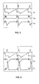
- FIGS. 4 to 6 also show the current I W2 through the second winding W2 and the drive voltages U T1 and U T2 for the first switch T1 and the second switch T2, respectively , So the control signals of the controller S2.
- the first switch T1 is turned on again at the latest with the zero crossing of the current I W1 .
- the feedback is, as I said, already possible because of the freewheeling diode of the switch T1.
- Turning on the first switch T1 then allows the new charging process, ie the further linear increase of the current I W1 .
- the rising edge of the signal U T2 is inclined, in contrast to the rising edge of the signal U T1 .
- the signal U T2 is obtained from a capacitor discharge with subsequent inversion, which entails the oblique rising shape.
- the switch-on time of the second switch T2 is not critical. It only has to be before the switch-off time of the first switch T1.
- a relatively early switching on of the second switch T2, as can be seen in FIG. 4, in this embodiment does not disturb the operations in the circuit until the opening of the first switch T1, because until then the corresponding induction voltages are polarized in such a way that the in FIG. 3 recognizable diode D5 blocks and thus the short circuit actually takes place only by the polarity change of the induction voltage when opening the first switch T1.
- the time duration of the charging phase (positive increase of I W1 )
- the duration of the voltage pulse U L and the return during the so-called Are essentially predetermined.
- the duration of the short-circuit phase which is effectively connected as a fourth phase between the first phase and the second phase, is freely selectable.
- the opening of the second switch T2 so the falling edge of the signal U T2 respond to an external trigger signal and thus allow a completely foreign-determined and, if necessary, aperiodic timing of the supply pulses U L.
- An internal timing of the circuit of Fig. 3 is not required.
- the trigger signal is indicated symbolically as line TR in FIG. 3 as the input of the drive circuit S2.
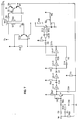
- Fig. 7 shows a more detailed circuit diagram for the principal in Fig. 3 shown circuit of the ballast according to the invention.
- Fig. 7 shows a more detailed circuit diagram for the principal in Fig. 3 shown circuit of the ballast according to the invention.
- a voltage source U V can be seen , which is applied as supply voltage U V to the recognizable in the right upper portion of the first winding W1.
- the arrows represented by the resistors R32, R2, R5, R4, R1, R54 and R37 and the collector of the transistor Q6 symbolize supply potentials derived from the supply voltage U V , all of which are positive and will not be discussed in detail.
- the first winding W1 is connected via the already mentioned first switch T1, a power MOSFET and a current measuring resistor (in the real version because of the current load a parallel circuit of shunt resistors) to ground.
- the first switch T1 is driven via a known driver circuit (so-called push-pull circuit) of two bipolar transistors Q10 and Q11, to which its gate is connected to the emitter of these driver transistors.
- the bases of the driver transistors Q10 and Q11 are connected together and lead to the drive circuit (S2 in FIG. 3) shown in the lower left-hand area of FIG. 7 and explained below.
- This connection can "pull down” the potential of the bases via diode D15. If this is not done, the potential of the bases is “pulled up” via the resistor R32 and the already mentioned voltage supply U V.
- FIG 7 shows the lamp circuit with the winding W3 and two terminals symbolizing the rest of the lamp circuit, between which the voltage U L is located.
- the "short circuit" can be seen in the upper right area of FIG. with the second winding W2 and the second switch T2 and the Diode D5. Again, it is a power MOSFET whose Gate is driven via a Bipolartreiberscrien Q6 and Q7. The bases of the bipolar transistors Q6 and Q7 are on one in the right area 7 down and at the bottom to the left leading line driven by the already mentioned drive circuit (S2 in Fig. 3). This via the diode D24.
- the drive circuit is in detail executed. From the left, the external trigger signal TR comes in and is through one from there up to and including the components R37 and Q4, d. H. until the connection the bases of the bipolar transistors Q6 and Q7 via D24, reaching Widened pulse shaping circuit. This is the rising edge over the Diode D2 and resistor R65 and the voltage-boosting transistor Q4 inverted, voltage-amplified and otherwise instantaneously let through.
- D3 denotes a Schottky diode for desaturation of the bipolar transistor Q4.
- the falling edge of the trigger pulse will over the substantially consisting of the resistor R34, and the capacitor C50 timer circuit time-delayed and inverted with this time delay and voltage-amplified passed.
- the capacitor C50 can be charged quickly via the diode D2, but over the Diode D1 and resistor R34 are discharged slowly.
- the initial edge of the trigger signal TR now falling through the inversion can thus lower the base potential of the driver transistors Q6 and Q7 through the diode D24 and thus open the second switch T2.
- the switch T2 remains open until the potential on the other side of the diode D24 has risen again as a result of the time delay, so that the diode D24 blocks and the bases are pulled up again via the resistor R1, whereby the second switch T2 is closed. This process corresponds to the oblique rise of the signal U T2 in Figs. 4-6.
- U2-B, U2-C, U2-D and U2-E denote inverting Schmitt triggers.
- Capacitor C53 between the output of Schmitttriggers U2-B and the Input of Schmitttriggers U2-C and resistor R54 form another Timer.
- the Schmitt trigger U2-B is the original polarity the trigger signal TR restored. Begins with its falling edge So to charge the capacitor C53, whose right port on the resistor R54 is at positive potential.
- the current through the first switch T1 that is to say the charging current I W1 is measured via the resistor R68.
- the corresponding voltage value is applied via a resistor R15 to the positive input of a comparator U3-B.
- At the negative input is formed by a variable resistor R3 and a resistor R5 reference voltage value V ref (via another resistor R16).
- the capacitor C9 is provided only for filtering.
- the output of the comparator thus becomes positive when the current I W1 exceeds a threshold defined by V ref . This is done strictly speaking on the resistor R4 and the supply potential connected via it, because the output of the comparator U3-B is high impedance after exceeding the threshold.
- the output of the comparator U3-B is low-resistance, so that the diode D9 blocks.
- the rising edge of the trigger signal TR leads to a total in the Essentially instantaneously to open the second switch T2.
- the second switch T2 is after the by the timer circuit given delay on the diode D24 closed again. This time delay can be seen in FIG. 4.
- the circuit shown forms the essential part of an electronic Ballast for a preferably rod-shaped dielectrically impeded Discharge lamp in a scanner with an optical CCD reader containing device, such as an electronic photocopier or a fax machine.
Landscapes
- Circuit Arrangements For Discharge Lamps (AREA)
- Dc-Dc Converters (AREA)
Abstract
Description
- Fig. 1
- zeigt ein stark vereinfachtes Schemaschaltbild für ein Vorschaltgerät für eine dielektrisch behinderte Entladungslampe nach dem Stand der Technik.
- Fig. 2
- zeigt Strom- und Spannungskurven zu Fig. 1.
- Fig. 3
- zeigt ein stark vereinfachtes Schaltdiagramm zu einem Vorschaltgerät gemäß der Erfindung.
- Fig. 4 - 6
- zeigen Strom- und Spannungsverläufe zu dem Vorschaltgerät aus Fig. 3.
- Fig. 7
- zeigt ein detaillierteres Schaltgerät zu dem Schaltdiagramm aus Fig. 3.
Claims (14)
- Elektronisches Vorschaltgerät für eine Lampe, insbesondere eine für dielektrisch behinderte Entladungen ausgelegte Lampe,
welches Vorschaltgerät eine Induktivität (W1 - W3) zur Erzeugung von iterativen Spannungspulsen (UL) in einem die Lampe enthaltenden Lampenkreis aufweist,
welche Induktivität (W1 - W3) eine über einen ersten steuerbaren Schalter (T1) von einer Spannungsquelle (UV) mit Strom (IW1) beaufschlagbare und durch den ersten Schalter (T1) von der Spannungsquelle (UV) trennbare erste Wicklung (W1) aufweist,
gekennzeichnet durch eine über einen steuerbaren zweiten Schalter (T2) niederohmig kurzschließbare und mit der ersten Wicklung (W1) gekoppelte zweite Wicklung (W2) der Induktivität (W1 - W3) zur Erzeugung einer Betriebsphase des Vorschaltgeräts, in der die zweite Wicklung (W2) niederohmig kurzgeschlossen ist. - Vorschaltgerät nach Anspruch 1, bei dem die Betriebsphase in Folge eines von außen in das Vorschaltgerät eingegebenen Triggersignals (TR) beendet werden kann.
- Vorschaltgerät nach Anspruch 2, dessen interne Zeitabläufe vollständig von dem Triggersignal (TR) abhängen.
- Vorschaltgerät nach einem der vorstehenden Ansprüche, bei dem die Induktivität ein Transformator (W1 - W3), vorzugsweise ein Trenntransformator ist.
- Vorschaltgerät nach einem der vorstehenden Ansprüche, welches zur Erzeugung der Spannungspulse (UL) als Sperrwandler ausgelegt ist.
- Vorschaltgerät nach Anspruch 5, das dazu ausgelegt ist, dass bei Trennung der ersten Wicklung (W1) von der Spannungsquelle (UV) durch Öffnen des ersten Schalters (T1) die zweite Wicklung (W2) durch den zweiten Schalter (T2) kurzgeschlossen ist, so dass die durch den Stromfluss der ersten Wicklung (W1) erzeugte Induktion durch einen Stromfluss durch die zweite Wicklung (W2) übernommen wird, und der zweite Schalter (T2) danach geöffnet wird, so dass in den Lampenkreis ein Spannungspuls (UL) eingeprägt wird.
- Vorschaltgerät nach einem der vorstehenden Ansprüche mit einem Zeitsteuerelement (C53) zum zeitgesteuerten Schließen des ersten Schalters (T1) nach dem Öffnen des zweiten Schalters (T2).
- Vorschaltgerät nach Anspruch 2 auch in Verbindung mit einem weiteren der vorstehenden Ansprüche mit einer Pulsformschaltung (D1, D2, C50, R34) zum Formen der Triggersignale (TR), wobei der Pulsbeginn des geformten Triggersignalpulses zum Öffnen und das Pulsende des geformten Triggersignalpulses zum Schließen des zweiten Schalters (T2) führt.
- Vorschaltgerät nach Anspruch 2 in Verbindung mit Anspruch 7 oder 8, welches eine bistabile Schaltung (U2-D, U2-E, D14) aufweist, die in Folge des Triggersignals (TR) durch die Zeitsteuerung (C53) gesetzt werden kann, um den ersten Schalter (T1) zu schließen, und mit einer Strommessschaltung (R3, R68, U3-B) zum Messen des Stromes (IW1) durch die erste Wicklung (W1), die die bistabile Schaltung (U2-D, U2-E, D14) umsetzen kann, um den ersten Schalter (T1) zu öffnen.
- Beleuchtungssystem aus einer für dielektrisch behinderte Entladungen ausgelegten Entladungslampe und einem Vorschaltgerät nach einem der vorstehenden Ansprüche zur Versorgung der Entladungslampe.
- Elektrisches Gerät, in dem ein Beleuchtungssystem nach Anspruch 10 verbaut ist und eine Triggersignalleitung (TR) für ein mit dem Betrieb des elektrischen Geräts abgestimmtes Triggersignal an dem Vorschaltgerät so angeschlossen ist, dass das Triggersignal (TR) zum Beenden der Betriebsphase des Vorschaltgeräts gemäß Anspruch 2 angelegt werden kann.
- Elektrisches Gerät nach Anspruch 11, das eine optische Leseeinrichtung aufweist, die die Entladungslampe enthält, wobei das Triggersignal (TR) auf einen Lesetakt der Leseeinrichtung abgestimmt ist.
- Verfahren zum Betreiben einer Lampe mit einem elektronischen Vorschaltgerät nach einem der Ansprüche 1 - 9, bei dem mit einer Induktivität (W1 - W3) iterative Spannungspulse (UL) in einem die Lampe enthaltenden Lampenkreis erzeugt werden, wobei eine erste Wicklung (W1) der Induktivität (W1 - W3) über Steuern eines ersten Schalters (T1) von einer Spannungsquelle (UV) mit Strom (IW1) beaufschlagt und von der Spannungsquelle (UV) getrennt wird,
dadurch gekennzeichnet, dass durch Steuern eines zweiten Schalters (T2) eine zweite Wicklung (W2) der Induktivität (W1 - W3) niederohmig kurzgeschlossen wird. - Verfahren zum Betreiben eines elektrischen Geräts nach Anspruch 11 oder 12 beinhaltend das Verfahren nach Anspruch 13 und das Abstimmen des Betriebs des Vorschaltgeräts auf den Betrieb des elektrischen Geräts durch Anlegen des Triggersignals (TR) an das Vorschaltgerät.
Applications Claiming Priority (2)
| Application Number | Priority Date | Filing Date | Title |
|---|---|---|---|
| DE10336857 | 2003-08-11 | ||
| DE10336857A DE10336857A1 (de) | 2003-08-11 | 2003-08-11 | Elektronisches Vorschaltgerät für eine mit iterativen Spannungspulsen zu betreibende Lampe |
Publications (2)
| Publication Number | Publication Date |
|---|---|
| EP1507446A1 true EP1507446A1 (de) | 2005-02-16 |
| EP1507446B1 EP1507446B1 (de) | 2006-09-27 |
Family
ID=33560292
Family Applications (1)
| Application Number | Title | Priority Date | Filing Date |
|---|---|---|---|
| EP04017003A Expired - Lifetime EP1507446B1 (de) | 2003-08-11 | 2004-07-19 | Elektronisches Vorschaltgerät für eine mit iterativen Spannungspulsen zu betreibende Lampe |
Country Status (8)
| Country | Link |
|---|---|
| US (1) | US7095184B2 (de) |
| EP (1) | EP1507446B1 (de) |
| JP (1) | JP4550520B2 (de) |
| KR (1) | KR101101428B1 (de) |
| CN (1) | CN1582081B (de) |
| CA (1) | CA2477367A1 (de) |
| DE (2) | DE10336857A1 (de) |
| TW (1) | TWI377873B (de) |
Cited By (1)
| Publication number | Priority date | Publication date | Assignee | Title |
|---|---|---|---|---|
| WO2011001339A1 (en) * | 2009-06-30 | 2011-01-06 | Koninklijke Philips Electronics N.V. | Circuit for converting dc into ac pulsed voltage |
Families Citing this family (7)
| Publication number | Priority date | Publication date | Assignee | Title |
|---|---|---|---|---|
| ITVI20030165A1 (it) * | 2003-08-11 | 2005-02-12 | Global Display Solutions Spa | Sistema di alimentazione elettrica |
| DE10336858A1 (de) * | 2003-08-11 | 2005-03-24 | Patent-Treuhand-Gesellschaft für elektrische Glühlampen mbH | Elektronisches Vorschaltgerät für eine mit iterativen Spannungspulsen zu betreibende Lampe |
| JP2006079848A (ja) * | 2004-09-07 | 2006-03-23 | Koito Mfg Co Ltd | スイッチング素子駆動回路及び放電灯点灯装置 |
| US20060087250A1 (en) * | 2004-10-25 | 2006-04-27 | Fiorello Ronald M | Method and circuit for igniting and powering a high intensity discharge lamp |
| JP2006331963A (ja) * | 2005-05-30 | 2006-12-07 | Ushio Inc | 放電ランプ点灯回路および放電ランプ点灯装置、光源装置 |
| DE102009053276A1 (de) * | 2009-11-13 | 2011-05-19 | Orlov, Walter, Dipl.-Ing. (FH) | Wechselspannung-Spannungsimpulse-Wandler |
| CN102958222B (zh) * | 2011-08-19 | 2016-09-28 | 国网安徽省电力公司阜阳供电公司 | 供电控制系统 |
Citations (3)
| Publication number | Priority date | Publication date | Assignee | Title |
|---|---|---|---|---|
| US3059143A (en) * | 1960-05-09 | 1962-10-16 | Basic Products Corp | Ballast for discharge devices |
| EP0671869A1 (de) * | 1994-03-09 | 1995-09-13 | General Electric Company | Vorschaltgerät für eine Lampe |
| US20020158589A1 (en) * | 2000-03-09 | 2002-10-31 | Lothar Hitzschke | Pulsed operation method for a silent discharge lamp |
Family Cites Families (6)
| Publication number | Priority date | Publication date | Assignee | Title |
|---|---|---|---|---|
| JPH0667110B2 (ja) * | 1985-06-25 | 1994-08-24 | 松下電工株式会社 | ヘアードライヤの漏電検出装置 |
| US4670662A (en) * | 1986-02-24 | 1987-06-02 | Gt-Devices | Pulse synthesizing network and method |
| US5945786A (en) | 1997-06-02 | 1999-08-31 | High End Systems, Inc. | Discharge lamp igniter with reduced noise output |
| JPH11283777A (ja) | 1998-03-31 | 1999-10-15 | Toshiba Lighting & Technology Corp | 放電ランプ点灯装置、放電ランプ装置および機器 |
| DE19839336A1 (de) * | 1998-08-28 | 2000-03-09 | Patent Treuhand Ges Fuer Elektrische Gluehlampen Mbh | Elektronisches Vorschaltgerät für Entladungslampe mit dielektrisch behinderten Entladungen |
| DE10336858A1 (de) * | 2003-08-11 | 2005-03-24 | Patent-Treuhand-Gesellschaft für elektrische Glühlampen mbH | Elektronisches Vorschaltgerät für eine mit iterativen Spannungspulsen zu betreibende Lampe |
-
2003
- 2003-08-11 DE DE10336857A patent/DE10336857A1/de not_active Withdrawn
-
2004
- 2004-07-19 EP EP04017003A patent/EP1507446B1/de not_active Expired - Lifetime
- 2004-07-19 DE DE502004001573T patent/DE502004001573D1/de not_active Expired - Lifetime
- 2004-08-03 US US10/909,393 patent/US7095184B2/en not_active Expired - Lifetime
- 2004-08-04 TW TW093123346A patent/TWI377873B/zh not_active IP Right Cessation
- 2004-08-10 CA CA002477367A patent/CA2477367A1/en not_active Abandoned
- 2004-08-10 KR KR1020040062855A patent/KR101101428B1/ko not_active Expired - Fee Related
- 2004-08-11 JP JP2004234863A patent/JP4550520B2/ja not_active Expired - Fee Related
- 2004-08-11 CN CN2004100566078A patent/CN1582081B/zh not_active Expired - Fee Related
Patent Citations (3)
| Publication number | Priority date | Publication date | Assignee | Title |
|---|---|---|---|---|
| US3059143A (en) * | 1960-05-09 | 1962-10-16 | Basic Products Corp | Ballast for discharge devices |
| EP0671869A1 (de) * | 1994-03-09 | 1995-09-13 | General Electric Company | Vorschaltgerät für eine Lampe |
| US20020158589A1 (en) * | 2000-03-09 | 2002-10-31 | Lothar Hitzschke | Pulsed operation method for a silent discharge lamp |
Cited By (1)
| Publication number | Priority date | Publication date | Assignee | Title |
|---|---|---|---|---|
| WO2011001339A1 (en) * | 2009-06-30 | 2011-01-06 | Koninklijke Philips Electronics N.V. | Circuit for converting dc into ac pulsed voltage |
Also Published As
| Publication number | Publication date |
|---|---|
| US20050035719A1 (en) | 2005-02-17 |
| CN1582081B (zh) | 2011-01-26 |
| CN1582081A (zh) | 2005-02-16 |
| CA2477367A1 (en) | 2005-02-11 |
| JP4550520B2 (ja) | 2010-09-22 |
| KR20050019040A (ko) | 2005-02-28 |
| US7095184B2 (en) | 2006-08-22 |
| EP1507446B1 (de) | 2006-09-27 |
| KR101101428B1 (ko) | 2012-01-02 |
| TW200518633A (en) | 2005-06-01 |
| TWI377873B (en) | 2012-11-21 |
| JP2005063972A (ja) | 2005-03-10 |
| DE502004001573D1 (de) | 2006-11-09 |
| DE10336857A1 (de) | 2005-03-10 |
Similar Documents
| Publication | Publication Date | Title |
|---|---|---|
| DE3877326T2 (de) | Leistungsversorgung. | |
| DE102004018823B3 (de) | Schaltungsanordnung mit einem Leistungstransistor und einer Ansteuerschaltung für den Leistungstransistor | |
| EP1057246A1 (de) | Gleichspannungs-/gleichspannungswandler mit einem transformator und einer drossel | |
| DE69125280T2 (de) | Verlustarmer Schwingkreis für Kapazitäts-Treiber | |
| DE3312209A1 (de) | Sperrschwinger-schaltnetzteil | |
| EP0756782B2 (de) | Gleichstrom-steuerschaltung | |
| EP1783910B1 (de) | Schaltungsanordnung und ein Verfahren zur galvanisch getrennten Ansteuerung eines Halbleiterschalters | |
| DE102005007346A1 (de) | Schaltungsanordnung und Verfahren zum Betreiben von Gasentladungslampen | |
| DE4013997C2 (de) | Gleichstrom-Steuerschaltung | |
| EP1507446B1 (de) | Elektronisches Vorschaltgerät für eine mit iterativen Spannungspulsen zu betreibende Lampe | |
| DE3813672C2 (de) | Wechselrichter für eine induktive Last | |
| DE3727117A1 (de) | Verfahren zur erzeugung einer niedrigen stabilisierten gleichspannung | |
| DE10000020A1 (de) | Integrierte Gate-Treiberschaltung | |
| EP1507445B1 (de) | Elektronisches Vorschaltgerät für eine mit iterativen Spannungspulsen zu betreibende Lampe | |
| EP2251979A1 (de) | Verfahren und Treiberschaltung zum Treiben eines Halbleiterleistungsschalters | |
| DE10240167B4 (de) | Schaltungsanordnung mit einem Leistungstransistor und einer Ansteuerschaltung für den Leistungstransistor | |
| DE3137940C2 (de) | Elektronisches Vorschaltgerät für mindestens eine Leuchtstofflampe | |
| DE19933161A1 (de) | Schaltungsanordnung | |
| DE2408181A1 (de) | Elektronische leistungssteuerungsvorrichtung | |
| DE3517297C1 (de) | Vorschaltgerät für Entladungslampen | |
| DE69020100T2 (de) | Speiseschaltung für Gleichspannungsregler mit spannungserhöhender Schaltanordnung. | |
| WO1990009518A1 (de) | Schaltungsanordnung und verfahren für das beschleunigte schalten von elektromagnetischen verbrauchern | |
| DE2719026A1 (de) | Schaltungsanordnung zur verringerung der ausschaltverluste in halbleiterschaltern | |
| EP0027171A1 (de) | Durchfluss-Gleichstromumrichter | |
| DE3736800C2 (de) |
Legal Events
| Date | Code | Title | Description |
|---|---|---|---|
| PUAI | Public reference made under article 153(3) epc to a published international application that has entered the european phase |
Free format text: ORIGINAL CODE: 0009012 |
|
| AK | Designated contracting states |
Kind code of ref document: A1 Designated state(s): AT BE BG CH CY CZ DE DK EE ES FI FR GB GR HU IE IT LI LU MC NL PL PT RO SE SI SK TR |
|
| AX | Request for extension of the european patent |
Extension state: AL HR LT LV MK |
|
| 17P | Request for examination filed |
Effective date: 20050307 |
|
| AKX | Designation fees paid |
Designated state(s): DE FR GB IT |
|
| GRAP | Despatch of communication of intention to grant a patent |
Free format text: ORIGINAL CODE: EPIDOSNIGR1 |
|
| GRAS | Grant fee paid |
Free format text: ORIGINAL CODE: EPIDOSNIGR3 |
|
| GRAA | (expected) grant |
Free format text: ORIGINAL CODE: 0009210 |
|
| AK | Designated contracting states |
Kind code of ref document: B1 Designated state(s): DE FR GB IT |
|
| PG25 | Lapsed in a contracting state [announced via postgrant information from national office to epo] |
Ref country code: IT Free format text: LAPSE BECAUSE OF FAILURE TO SUBMIT A TRANSLATION OF THE DESCRIPTION OR TO PAY THE FEE WITHIN THE PRESCRIBED TIME-LIMIT;WARNING: LAPSES OF ITALIAN PATENTS WITH EFFECTIVE DATE BEFORE 2007 MAY HAVE OCCURRED AT ANY TIME BEFORE 2007. THE CORRECT EFFECTIVE DATE MAY BE DIFFERENT FROM THE ONE RECORDED. Effective date: 20060927 |
|
| REG | Reference to a national code |
Ref country code: GB Ref legal event code: FG4D Free format text: NOT ENGLISH |
|
| REF | Corresponds to: |
Ref document number: 502004001573 Country of ref document: DE Date of ref document: 20061109 Kind code of ref document: P |
|
| GBT | Gb: translation of ep patent filed (gb section 77(6)(a)/1977) |
Effective date: 20070103 |
|
| ET | Fr: translation filed | ||
| PLBE | No opposition filed within time limit |
Free format text: ORIGINAL CODE: 0009261 |
|
| STAA | Information on the status of an ep patent application or granted ep patent |
Free format text: STATUS: NO OPPOSITION FILED WITHIN TIME LIMIT |
|
| 26N | No opposition filed |
Effective date: 20070628 |
|
| PGRI | Patent reinstated in contracting state [announced from national office to epo] |
Ref country code: IT Effective date: 20081001 |
|
| PGFP | Annual fee paid to national office [announced via postgrant information from national office to epo] |
Ref country code: FR Payment date: 20090717 Year of fee payment: 6 |
|
| PGFP | Annual fee paid to national office [announced via postgrant information from national office to epo] |
Ref country code: GB Payment date: 20090713 Year of fee payment: 6 |
|
| PGFP | Annual fee paid to national office [announced via postgrant information from national office to epo] |
Ref country code: IT Payment date: 20090728 Year of fee payment: 6 |
|
| GBPC | Gb: european patent ceased through non-payment of renewal fee |
Effective date: 20100719 |
|
| REG | Reference to a national code |
Ref country code: FR Ref legal event code: ST Effective date: 20110331 |
|
| PG25 | Lapsed in a contracting state [announced via postgrant information from national office to epo] |
Ref country code: IT Free format text: LAPSE BECAUSE OF NON-PAYMENT OF DUE FEES Effective date: 20100719 Ref country code: FR Free format text: LAPSE BECAUSE OF NON-PAYMENT OF DUE FEES Effective date: 20100802 |
|
| PG25 | Lapsed in a contracting state [announced via postgrant information from national office to epo] |
Ref country code: GB Free format text: LAPSE BECAUSE OF NON-PAYMENT OF DUE FEES Effective date: 20100719 |
|
| REG | Reference to a national code |
Ref country code: DE Ref legal event code: R081 Ref document number: 502004001573 Country of ref document: DE Owner name: OSRAM GMBH, DE Free format text: FORMER OWNER: OSRAM GESELLSCHAFT MIT BESCHRAENKTER HAFTUNG, 81543 MUENCHEN, DE Effective date: 20111213 |
|
| REG | Reference to a national code |
Ref country code: DE Ref legal event code: R081 Ref document number: 502004001573 Country of ref document: DE Owner name: OSRAM GMBH, DE Free format text: FORMER OWNER: OSRAM AG, 81543 MUENCHEN, DE Effective date: 20130205 |
|
| REG | Reference to a national code |
Ref country code: DE Ref legal event code: R081 Ref document number: 502004001573 Country of ref document: DE Owner name: OSRAM GMBH, DE Free format text: FORMER OWNER: OSRAM GMBH, 81543 MUENCHEN, DE Effective date: 20130822 |
|
| PGFP | Annual fee paid to national office [announced via postgrant information from national office to epo] |
Ref country code: DE Payment date: 20170724 Year of fee payment: 14 |
|
| REG | Reference to a national code |
Ref country code: DE Ref legal event code: R119 Ref document number: 502004001573 Country of ref document: DE |
|
| PG25 | Lapsed in a contracting state [announced via postgrant information from national office to epo] |
Ref country code: DE Free format text: LAPSE BECAUSE OF NON-PAYMENT OF DUE FEES Effective date: 20190201 |