EP1503907B1 - Element optiquement variable comportant une serie de couches constituees d'un film mince - Google Patents
Element optiquement variable comportant une serie de couches constituees d'un film mince Download PDFInfo
- Publication number
- EP1503907B1 EP1503907B1 EP03718769A EP03718769A EP1503907B1 EP 1503907 B1 EP1503907 B1 EP 1503907B1 EP 03718769 A EP03718769 A EP 03718769A EP 03718769 A EP03718769 A EP 03718769A EP 1503907 B1 EP1503907 B1 EP 1503907B1
- Authority
- EP
- European Patent Office
- Prior art keywords
- layer
- optically variable
- variable element
- film
- partial
- Prior art date
- Legal status (The legal status is an assumption and is not a legal conclusion. Google has not performed a legal analysis and makes no representation as to the accuracy of the status listed.)
- Expired - Lifetime
Links
- 239000010409 thin film Substances 0.000 title claims abstract description 107
- 238000004049 embossing Methods 0.000 claims abstract description 10
- 238000010030 laminating Methods 0.000 claims abstract description 6
- 239000010410 layer Substances 0.000 claims description 411
- 238000010521 absorption reaction Methods 0.000 claims description 42
- 229910052751 metal Inorganic materials 0.000 claims description 40
- 239000002184 metal Substances 0.000 claims description 40
- 125000006850 spacer group Chemical group 0.000 claims description 34
- 239000012790 adhesive layer Substances 0.000 claims description 19
- 239000004922 lacquer Substances 0.000 claims description 16
- 239000010408 film Substances 0.000 claims description 15
- 230000000694 effects Effects 0.000 claims description 14
- 230000001681 protective effect Effects 0.000 claims description 13
- 239000011888 foil Substances 0.000 abstract description 6
- 239000000463 material Substances 0.000 description 23
- 238000000034 method Methods 0.000 description 19
- 230000003287 optical effect Effects 0.000 description 18
- 238000005530 etching Methods 0.000 description 17
- 230000010076 replication Effects 0.000 description 14
- 238000002679 ablation Methods 0.000 description 9
- 238000007740 vapor deposition Methods 0.000 description 9
- 238000007639 printing Methods 0.000 description 7
- 230000005540 biological transmission Effects 0.000 description 6
- 238000004519 manufacturing process Methods 0.000 description 6
- 238000001465 metallisation Methods 0.000 description 6
- PXHVJJICTQNCMI-UHFFFAOYSA-N Nickel Chemical compound [Ni] PXHVJJICTQNCMI-UHFFFAOYSA-N 0.000 description 5
- 230000001419 dependent effect Effects 0.000 description 5
- XEEYBQQBJWHFJM-UHFFFAOYSA-N Iron Chemical compound [Fe] XEEYBQQBJWHFJM-UHFFFAOYSA-N 0.000 description 4
- 239000000758 substrate Substances 0.000 description 4
- 229910052782 aluminium Inorganic materials 0.000 description 3
- 229910052804 chromium Inorganic materials 0.000 description 3
- 239000011651 chromium Substances 0.000 description 3
- 229910052759 nickel Inorganic materials 0.000 description 3
- 238000000926 separation method Methods 0.000 description 3
- 239000002966 varnish Substances 0.000 description 3
- VYZAMTAEIAYCRO-UHFFFAOYSA-N Chromium Chemical compound [Cr] VYZAMTAEIAYCRO-UHFFFAOYSA-N 0.000 description 2
- UQSXHKLRYXJYBZ-UHFFFAOYSA-N Iron oxide Chemical compound [Fe]=O UQSXHKLRYXJYBZ-UHFFFAOYSA-N 0.000 description 2
- KDLHZDBZIXYQEI-UHFFFAOYSA-N Palladium Chemical compound [Pd] KDLHZDBZIXYQEI-UHFFFAOYSA-N 0.000 description 2
- XAGFODPZIPBFFR-UHFFFAOYSA-N aluminium Chemical compound [Al] XAGFODPZIPBFFR-UHFFFAOYSA-N 0.000 description 2
- 238000010276 construction Methods 0.000 description 2
- 229910052802 copper Inorganic materials 0.000 description 2
- 239000010949 copper Substances 0.000 description 2
- 238000009760 electrical discharge machining Methods 0.000 description 2
- 229910052737 gold Inorganic materials 0.000 description 2
- 239000010931 gold Substances 0.000 description 2
- 238000010849 ion bombardment Methods 0.000 description 2
- 229910052742 iron Inorganic materials 0.000 description 2
- 238000000608 laser ablation Methods 0.000 description 2
- PQXKHYXIUOZZFA-UHFFFAOYSA-M lithium fluoride Chemical compound [Li+].[F-] PQXKHYXIUOZZFA-UHFFFAOYSA-M 0.000 description 2
- 239000000203 mixture Substances 0.000 description 2
- 239000000049 pigment Substances 0.000 description 2
- 229910052709 silver Inorganic materials 0.000 description 2
- IRPGOXJVTQTAAN-UHFFFAOYSA-N 2,2,3,3,3-pentafluoropropanal Chemical compound FC(F)(F)C(F)(F)C=O IRPGOXJVTQTAAN-UHFFFAOYSA-N 0.000 description 1
- KLZUFWVZNOTSEM-UHFFFAOYSA-K Aluminum fluoride Inorganic materials F[Al](F)F KLZUFWVZNOTSEM-UHFFFAOYSA-K 0.000 description 1
- OKTJSMMVPCPJKN-UHFFFAOYSA-N Carbon Chemical compound [C] OKTJSMMVPCPJKN-UHFFFAOYSA-N 0.000 description 1
- RYGMFSIKBFXOCR-UHFFFAOYSA-N Copper Chemical compound [Cu] RYGMFSIKBFXOCR-UHFFFAOYSA-N 0.000 description 1
- ZOKXTWBITQBERF-UHFFFAOYSA-N Molybdenum Chemical compound [Mo] ZOKXTWBITQBERF-UHFFFAOYSA-N 0.000 description 1
- VYPSYNLAJGMNEJ-UHFFFAOYSA-N Silicium dioxide Chemical compound O=[Si]=O VYPSYNLAJGMNEJ-UHFFFAOYSA-N 0.000 description 1
- BQCADISMDOOEFD-UHFFFAOYSA-N Silver Chemical compound [Ag] BQCADISMDOOEFD-UHFFFAOYSA-N 0.000 description 1
- RTAQQCXQSZGOHL-UHFFFAOYSA-N Titanium Chemical compound [Ti] RTAQQCXQSZGOHL-UHFFFAOYSA-N 0.000 description 1
- 239000000956 alloy Substances 0.000 description 1
- 229910045601 alloy Inorganic materials 0.000 description 1
- 238000013459 approach Methods 0.000 description 1
- OYLGJCQECKOTOL-UHFFFAOYSA-L barium fluoride Chemical compound [F-].[F-].[Ba+2] OYLGJCQECKOTOL-UHFFFAOYSA-L 0.000 description 1
- 229910001632 barium fluoride Inorganic materials 0.000 description 1
- WUKWITHWXAAZEY-UHFFFAOYSA-L calcium difluoride Chemical compound [F-].[F-].[Ca+2] WUKWITHWXAAZEY-UHFFFAOYSA-L 0.000 description 1
- 229910001634 calcium fluoride Inorganic materials 0.000 description 1
- 229910052799 carbon Inorganic materials 0.000 description 1
- 150000004770 chalcogenides Chemical class 0.000 description 1
- 229910017052 cobalt Inorganic materials 0.000 description 1
- 239000010941 cobalt Substances 0.000 description 1
- GUTLYIVDDKVIGB-UHFFFAOYSA-N cobalt atom Chemical compound [Co] GUTLYIVDDKVIGB-UHFFFAOYSA-N 0.000 description 1
- 238000005260 corrosion Methods 0.000 description 1
- 230000007797 corrosion Effects 0.000 description 1
- 238000005516 engineering process Methods 0.000 description 1
- PCHJSUWPFVWCPO-UHFFFAOYSA-N gold Chemical compound [Au] PCHJSUWPFVWCPO-UHFFFAOYSA-N 0.000 description 1
- 230000010354 integration Effects 0.000 description 1
- ORUIBWPALBXDOA-UHFFFAOYSA-L magnesium fluoride Chemical compound [F-].[F-].[Mg+2] ORUIBWPALBXDOA-UHFFFAOYSA-L 0.000 description 1
- 229910001635 magnesium fluoride Inorganic materials 0.000 description 1
- 150000002739 metals Chemical class 0.000 description 1
- 229910052750 molybdenum Inorganic materials 0.000 description 1
- 239000011733 molybdenum Substances 0.000 description 1
- TWNQGVIAIRXVLR-UHFFFAOYSA-N oxo(oxoalumanyloxy)alumane Chemical compound O=[Al]O[Al]=O TWNQGVIAIRXVLR-UHFFFAOYSA-N 0.000 description 1
- 229910052763 palladium Inorganic materials 0.000 description 1
- 238000007650 screen-printing Methods 0.000 description 1
- 229910052814 silicon oxide Inorganic materials 0.000 description 1
- 239000004332 silver Substances 0.000 description 1
- 239000010944 silver (metal) Substances 0.000 description 1
- 238000010572 single replacement reaction Methods 0.000 description 1
- 150000004763 sulfides Chemical class 0.000 description 1
- 239000010936 titanium Substances 0.000 description 1
- 229910052719 titanium Inorganic materials 0.000 description 1
- 239000012780 transparent material Substances 0.000 description 1
- WFKWXMTUELFFGS-UHFFFAOYSA-N tungsten Chemical compound [W] WFKWXMTUELFFGS-UHFFFAOYSA-N 0.000 description 1
- 229910052721 tungsten Inorganic materials 0.000 description 1
- 239000010937 tungsten Substances 0.000 description 1
- 238000005406 washing Methods 0.000 description 1
Images


Classifications
-
- B—PERFORMING OPERATIONS; TRANSPORTING
- B42—BOOKBINDING; ALBUMS; FILES; SPECIAL PRINTED MATTER
- B42D—BOOKS; BOOK COVERS; LOOSE LEAVES; PRINTED MATTER CHARACTERISED BY IDENTIFICATION OR SECURITY FEATURES; PRINTED MATTER OF SPECIAL FORMAT OR STYLE NOT OTHERWISE PROVIDED FOR; DEVICES FOR USE THEREWITH AND NOT OTHERWISE PROVIDED FOR; MOVABLE-STRIP WRITING OR READING APPARATUS
- B42D25/00—Information-bearing cards or sheet-like structures characterised by identification or security features; Manufacture thereof
- B42D25/30—Identification or security features, e.g. for preventing forgery
- B42D25/328—Diffraction gratings; Holograms
-
- B—PERFORMING OPERATIONS; TRANSPORTING
- B42—BOOKBINDING; ALBUMS; FILES; SPECIAL PRINTED MATTER
- B42D—BOOKS; BOOK COVERS; LOOSE LEAVES; PRINTED MATTER CHARACTERISED BY IDENTIFICATION OR SECURITY FEATURES; PRINTED MATTER OF SPECIAL FORMAT OR STYLE NOT OTHERWISE PROVIDED FOR; DEVICES FOR USE THEREWITH AND NOT OTHERWISE PROVIDED FOR; MOVABLE-STRIP WRITING OR READING APPARATUS
- B42D25/00—Information-bearing cards or sheet-like structures characterised by identification or security features; Manufacture thereof
- B42D25/20—Information-bearing cards or sheet-like structures characterised by identification or security features; Manufacture thereof characterised by a particular use or purpose
- B42D25/21—Information-bearing cards or sheet-like structures characterised by identification or security features; Manufacture thereof characterised by a particular use or purpose for multiple purposes
-
- B—PERFORMING OPERATIONS; TRANSPORTING
- B41—PRINTING; LINING MACHINES; TYPEWRITERS; STAMPS
- B41M—PRINTING, DUPLICATING, MARKING, OR COPYING PROCESSES; COLOUR PRINTING
- B41M3/00—Printing processes to produce particular kinds of printed work, e.g. patterns
- B41M3/14—Security printing
-
- B—PERFORMING OPERATIONS; TRANSPORTING
- B42—BOOKBINDING; ALBUMS; FILES; SPECIAL PRINTED MATTER
- B42D—BOOKS; BOOK COVERS; LOOSE LEAVES; PRINTED MATTER CHARACTERISED BY IDENTIFICATION OR SECURITY FEATURES; PRINTED MATTER OF SPECIAL FORMAT OR STYLE NOT OTHERWISE PROVIDED FOR; DEVICES FOR USE THEREWITH AND NOT OTHERWISE PROVIDED FOR; MOVABLE-STRIP WRITING OR READING APPARATUS
- B42D25/00—Information-bearing cards or sheet-like structures characterised by identification or security features; Manufacture thereof
- B42D25/20—Information-bearing cards or sheet-like structures characterised by identification or security features; Manufacture thereof characterised by a particular use or purpose
- B42D25/29—Securities; Bank notes
-
- G—PHYSICS
- G07—CHECKING-DEVICES
- G07D—HANDLING OF COINS OR VALUABLE PAPERS, e.g. TESTING, SORTING BY DENOMINATIONS, COUNTING, DISPENSING, CHANGING OR DEPOSITING
- G07D7/00—Testing specially adapted to determine the identity or genuineness of valuable papers or for segregating those which are unacceptable, e.g. banknotes that are alien to a currency
- G07D7/06—Testing specially adapted to determine the identity or genuineness of valuable papers or for segregating those which are unacceptable, e.g. banknotes that are alien to a currency using wave or particle radiation
- G07D7/12—Visible light, infrared or ultraviolet radiation
-
- B42D2035/24—
Definitions
- the invention relates to an optically variable element, in particular an optically variable fuse element for securing banknotes, credit cards and the like, which has a thin film for generating color shifts by means of interference.
- the invention further relates to a security product and a film, in particular an embossing film or laminating film, which has such an optically variable element.
- Optically variable elements are often used to complicate and, where possible, prevent the copying and misuse of documents or products.
- optically variable elements are often used for securing documents, banknotes, credit cards, cash cards and the like.
- WO 01/03945 A1 describes a security product comprising a transparent substrate, on one side of which a thin film is applied, which produces a perceptible color shift as a function of the viewing angle change.
- the thin film consists of an absorption layer deposited on the transparent substrate and a dielectric layer deposited on the absorption layer.
- the absorption layer contains a material which is composed of one of the following materials or a combination of these materials: chromium, nickel, palladium, titanium, cobalt, iron, tungsten, molybdenum, iron oxide or carbon.
- the dielectric layer is made of any of the following materials or a combination of the following materials: silicon oxide, aluminum oxide, magnesium fluoride, aluminum fluoride, barium fluoride, calcium fluoride or lithium fluoride.
- a diffraction pattern is impressed on the side of the transparent substrate opposite the thin-film layer sequence.
- This diffraction pattern acts as a diffraction grating, so that by means of this two-dimensional pattern, e.g. create the illusion of a three-dimensional image for the viewer.
- an optically variable element is achieved that at each point of the optically variable element by the Thin film layers generated optical effects and superimpose the optical effects generated by the diffractive pattern and thus results in an overall optical effect that is difficult to imitate and copy.
- the optically variable element here consists of several layers, which are arranged one above the other.
- the optically variable element has, on the one hand, a thin film which generates the above-described optical effect of a viewing angle-dependent color change.
- the optically variable element has a replication layer into which a relief structure is embossed. This relief structure produces a further optical effect, namely the diffraction effect already described above, by means of which holograms and the like can be represented.
- the thin-film layers are first applied to the replication layer and then the relief structure is impressed.
- WO 02/00445 A1 describes that the optical effect produced by the thin-film structure and the optical effect generated by the relief structure are decoupled from one another. Two approaches are proposed for this.
- the relief structure which produces a holographic image by means of diffraction
- the thin film which produces a color-changing effect.
- the relief structure is shielded from the thin-film structure.
- the second possibility is to form two or more layers of substantially transparent material between the diffraction-generating holographic images Relief structure and the thin film layers to arrange. These layers may comprise one or more high-index layers and an adhesive layer. By means of these layers, the reflection and thus the light intensity in the region of the holographic image-forming relief structure is increased.
- variable optical element can be produced as follows: First, a pattern is embossed in a holographic film. This film is then provided in regions with a metal layer. Then, the thin-film layers are successively evaporated. Finally, a full-surface metal layer is applied.
- Another possibility is to provide a prefabricated thin-film layer sequence with a sealable lacquer and then impress the relief structure in this lacquer. It is further proposed to bond such prefabricated thin-film layers with prefabricated microstructures.
- WO 02/00445 A1 thus describes either the use of security elements in which the optical effect generated by diffractive structures and the optical effect produced by thin-film structures are coupled together, or to use security elements in which the optical effect produced by diffractive structures and that produced by thin-film layers optical effect are decoupled from each other.
- the invention is based on the object of complicating the copying and copying of optically variable elements and thus to improve the counterfeit security of security products.
- an optically variable element in particular an optically variable fuse element for securing banknotes, credit cards and the like, which has a thin film for generating color shifts by means of interference and a further layer, wherein the thin film is formed as a partial thin film element, the Surface area of the further layer only partially covered and patterned.
- This object is further achieved by a security product and by a film, in particular an embossing film or laminating film, which has such an optically variable element.
- the invention achieves the advantage that an optically variable element according to the invention can be copied much more severely than the optically variable elements known in the prior art.
- the security against counterfeiting of security products equipped with an optically variable element configured according to the invention increases considerably.
- the security against counterfeiting is greatly increased.
- the optically variable element described in WO 02/00445 A1 - as described in WO 02 / 00445A1 as a possibility of production - be imitated by processing a prefabricated thin-film foil with an embossing stamp, with which a diffractive structure is embossed into the thin-film foil becomes.
- This is no longer possible in the case of an optically variable element designed according to the invention.
- the partial application of a thin-film layer sequence which produces a color shift by means of interference requires a high level of technological effort.
- the partial thin-film element thus produced, compared to a prefabricated thin-film foil, represents an individualized element, so that it is no longer possible to imitate the optically variable element starting from a prefabricated thin-film layer sequence.
- the further layer is preferably a continuous protective lacquer layer, a continuous reflective layer or a continuous adhesive layer.
- the further layer it is not necessary for the further layer to cover the entire surface area of the optically variable element.
- additional additional layers may be provided, the surface areas of which are covered only partially and in pattern form by the partial thin-film element.
- the variable optical element has a continuous protective lacquer layer, a continuous reflection layer and a continuous adhesive layer.
- the partial thin-film element it is expedient to build up the partial thin-film element from an absorption layer and a spacer layer. Further, it is possible to construct the partial thin film element of a larger number of layers having mutually different refractive indices.
- the security against counterfeiting can be further increased by virtue of the fact that the partial thin-film element has a reflective layer, preferably a metal layer, having. This improves the visibility of the partial thin film element.
- the partial thin-film element with a transmission layer.
- the partial thin-film element with a diffractive structure as an additional security element.
- a diffractive structure for example, diffraction effects can be achieved by means of which, for example, holograms or defined color effects can be produced.
- the imitation of the optically variable element can be made more difficult by the fact that the partial thin-film element is provided with a partial reflective layer, in particular a metal layer, which only partially covers the surface area of the partial thin-film element.
- a partial reflective layer in particular a metal layer, which only partially covers the surface area of the partial thin-film element.
- a metal layer which only partially covers the surface area of the partial thin-film element.
- a possibility associated with manufacturing advantages of designing a surface region of the optically variable element delimited by the partial thin-film element consists in applying an absorption layer, but not a spacer layer, in this surface region. These advantages are further achieved by providing a spacer layer, but not an absorption layer, in the area of the optically variable element bounded by the partial thin film element.
- this area bounded by the partial thin film element is enclosed by the partial thin film element or encloses the thin film element.
- Advantages for the subsequent layer structure can result from the fact that the total layer thickness of the one or more replacement layers corresponds approximately to the layer thickness of the partial thin-film element.
- the imitation of the optically variable element can be further complicated by providing one of the one or more replacement layers with a diffractive structure. This advantage is further achieved in that a reflection layer and a carrier layer are applied as substitute layers. Alternatively, it is also possible to apply a single replacement layer in which it For example, it is a reflection layer. Such a procedure, as explained below, be associated with manufacturing advantages.
- the design of the one or more replacement layers it is also advantageous for the design of the one or more replacement layers that they have a partial reflective layer that only partially covers the surface area of the one or more replacement layers.
- a partial reflective layer that only partially covers the surface area of the one or more replacement layers.
- An optically variable element according to the invention can thus have a multiplicity of combinations of valuable security features and offers a multiplicity of appealing design features.
- the optically variable element 0 is intended to be applied to a security product, for example a banknote, a credit card, a cash card or a document. It is also possible that the optically variable element is intended to be applied as a security or authenticity marking on an object, for example on a CD, or on a package.
- a security product for example a banknote, a credit card, a cash card or a document. It is also possible that the optically variable element is intended to be applied as a security or authenticity marking on an object, for example on a CD, or on a package.
- the optically variable element 0 can take many forms.
- the optically variable element 0 may thus be, for example, a security thread intended to be applied to one of the objects specified above.
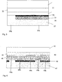
- Fig. 1 shows a carrier 1 and five layers 2 to 6.
- the optically variable element 0 is formed by the layers 2 to 6.
- the layer 2 is a protective lacquer and / or release layer
- the layer 3 is an absorption layer
- the layer 4 is a spacer layer.
- the layer 6 is an adhesive layer.
- the carrier 1 consists for example of PET.
- the carrier serves the manufacturing structure of the optically variable element. During or after the application of the optically variable element to the object to be secured, the carrier 1 is removed. In Fig. 1, the optically variable element is thus shown in a state in which it is part of a film, for example an embossing film or a laminating film.
- the layer 2 has an adhesion-promoting layer.
- a thin film is distinguished in principle by an interference layer structure which generates viewing angle-dependent color shifts. It can be constructed as a reflective element, with, for example, highly reflective metal layers or as a transmissive element with a transparent optical separation layer (higher refractive index (HRI) or lower refractive index (LRI)) to the adjacent layers.
- the basic structure of the thin film has an absorption layer (preferably with 30% to 65% transmission), a transparent spacer layer as a color change-generating layer (eg ⁇ -quarter or ⁇ -half layer) and a metal layer as a reflective or an optical separation layer as a transmitting layer.
- the layers 3, 4 and 5, ie the absorption layer, the spacer layer and the metal layer or HRI layer form a thin film which generates viewing angle-dependent color shifts by means of interference.
- the color shifts produced by the thin film are preferably in the range of the light visible to a human observer.
- this thin film is formed as a partial thin film element covering the area of the optically variable element O only in regions and in a pattern.
- the layer thickness of the spacer layer 4 is to be selected such that the ⁇ / 4 condition is fulfilled. If the layer 5 consists of a transmissive layer, then the spacer layer 4 has to fulfill the ⁇ / 2 condition.
- the partial thin film element is composed of a sequence of high and low refractive layers.
- the partial thin film element may be composed of 3 to 9 such layers (odd number of thin film layers) or 2 to 10 such layers (even number of thin film layers). The higher the number of layers, the sharper the wavelength can be set for the color change effect.
- the layer 5 may be formed as a full-area or as a partial metal layer or HRI layer. Suitable materials for the layer 5 are, for example, Al, Ag, Cr, Ni, Cu, Au or combinations of reflective metals.
- the layer 5 can have a structured surface. It can thus have a diffractive structure, a refractive structure (lenses) or macroscopic structures (greater than 30 ⁇ m). Furthermore, it can also have an unstructured reflective or scattering surface.
- optically variable element 0 may have one or more further layers.
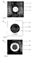
- the optically variable element 10 has three surface areas 11 to 13, the optically variable element 20 three surface areas 21 to 23 and the optically variable element 30 three surface areas 31 up to 33 on.
- the areas 12, 23 and 31 of the optically variable elements 10, 20 and 30 are each covered by a partial thin film element.
- the partial thin-film element is shaped in each case in regions and in a pattern.
- the respective partial thin-film element prefferably be transmissive or reflective.
- a partial, pattern-like both transmissive and reflective design within the respective surface area further interesting effects can be achieved.
- the surface regions 12, 23 and 31 can also be provided with a diffractive structure.
- the surface areas 11, 22 and 33 of the optically variable elements 10, 20 and 30 are each covered with a partial metallization. These areas can also be provided with a diffractive structure.
- a transparent window is visible in each case.
- the transparent windows each have a partial transparent element.
- This has transparent or transmissive properties (clearcoat compositions, oxidic, partially metallized, scattering transmissive organic and inorganic compositions). These areas can also be provided with a diffractive structure.
- FIGS. 2a to 2c can all be executed relative to one another in the register and can include, without limitation of generality, graphic elements, alphanumeric and geometric symbols, barcodes and random patterns and their combinations.
- Fig. 3 illustrates one way to construct an optically variable element provided with a partial thin film element.
- Fig. 3 shows a carrier 31, five layers 32 to 37 and two surface areas 39a and 39b.
- the layer 32 is a protective lacquer and / or release layer
- the layer 33 is a replication layer, which is formed, for example, by a replication lacquer.
- the layer 36 is formed by an etch resist.
- the layer 37 is an adhesive layer.
- the protective lacquer and release layer 32, the replication layer 33 and the metal layer 35 are applied over the entire area on the carrier 31.
- the layer 35 is then partially provided with diffractive structures by means of an embossing tool.
- the metal layer 35 is printed with an etching resist, so that the only partially formed layer 36 is formed.
- the surface not covered by the etch resist is removed by etching.
- ablation methods such as laser ablation, spark erosion, plasma or ion bombardment.
- ablation methods make it possible to transmit digitally stored images, texts and codes.
- the layers of the partial thin-film element can be applied by vapor deposition with appropriately shaped vapor-deposition masks or by printing the layers in the region of the interspaces.
- FIG. 4 shows an optically variable element in which a surface area of the optically variable element delimited by a partial thin-film element has a spacer layer but no absorption layer.
- FIG. 4 shows a carrier 41, five layers 42 to 47 and a plurality of surface regions 49a and 49b.
- the layer 42 is a protective lacquer and / or release layer, the layer 43 is an absorption layer.
- the layer 44 is a spacer layer.
- the layer 47 is an adhesive layer.
- the protective lacquer and release layer 42 and the absorption layer 43 are applied over the entire surface of the support 41.
- the absorption layer 43 can be vapor-deposited or applied by a printing process.
- the absorption layer is partially removed in the surface regions 49b.
- This partial removal of the absorption layer is carried out by positive etching or negative etching.
- an etchant can be applied as a pattern by a printing process, for example by means of a roller or by screen printing.
- an etching mask can be applied, which is removed by a washing process after the etching process.
- ablation methods such as laser ablation, spark erosion, plasma or ion bombardment.
- the absorption layer instead of applying the entire surface of the absorption layer, it is also possible to apply the absorption layer only partially to the layer 42. This can be done by vapor deposition by means of pattern-shaped vapor deposition masks or by a corresponding pattern-shaped printing of the absorption layer 43 on the layer 42.
- the spacer layer 44 is now applied over the entire surface.
- the application of the spacer layer may e.g. by vapor deposition or by the full-surface imprint of the absorption layer.
- the surface areas 49a are covered after this process with a thin film consisting of the absorption layer 43 and the spacer layer 44.
- This thin film generates (after the application of the further layers, which act as optical separation layers) with a corresponding light incidence viewing angle-dependent color shifts by means of interference.
- the absorption layer 43 is missing, so that such color shifts can not be generated there.
- the surface regions of the optically variable element delimited by the partial thin-film element may have an absorption layer but not a spacer layer.
- the absorption layer for example, by vapor deposition or printing, is applied over the entire surface. Subsequently, the spacer layer is applied only partially by a printing process. Again, there is the possibility that the spacer layer is applied over the entire surface and then by one of the methods described above (positive etching, negative etching, ablation) is removed.
- the layer 46 is a reflection layer, then it preferably consists of a metal. This metal can also be colored. As materials are essentially chromium, aluminum, copper, iron, nickel, silver, gold or an alloy with these materials in question.
- the layer 46 it is possible to carry out the layer 46 as a partial metal layer. Again, it is possible, the layer 46 only full area z. B. by vapor deposition, apply and then by one of the methods described above (positive etching, negative etching, ablation) to remove. If metal pigments are used as the reflective layer, then this layer can be partially printed, which then results in a partial reflective layer.
- the layer 46 is formed as a transmission layer, in particular materials such as oxides, sulfides or chalcogenides are suitable as materials for this layer.
- materials such as oxides, sulfides or chalcogenides are suitable as materials for this layer.
- Critical to the choice of materials is that there is a difference in refractive index over the materials used in the spacer layer 44. This difference should not be less than 0.2.
- an HRI material or an LRI material for the layer 46 will be used.
- the transmission layer can in this case also be formed by an adhesive layer which fulfills this condition with respect to the refractive indices.
- an above-described “extinguishing effect” can be achieved further.
- a layer eg, an adhesive layer
- adhering to the spacer layer which does not satisfy the above-described refractive index condition is added, the optical thickness of the spacer layer is increased and the visible interference effect no longer occurs.
- the layer 5a shows a carrier 51, eight layers 52 to 59 and a plurality of surface regions 59a and 59b.
- the layer 52 is a protective lacquer and / or release layer.
- the layer 53 is a replication layer.
- the layer 54 is an absorption layer.
- the layers 56 and 57 are spare layers.
- the layer 59 is an adhesive layer.
- the layers 52, 53, 54, 55, 58 and 59 are designed as described in the exemplary embodiments according to FIGS. 3 and 4 and are applied to the carrier 51 as described there.
- the layer 53 consists of a replicate varnish or of a thermoformable plastic.
- diffractive structures are now impressed in the surface areas between the partial thin-film layer. This embossing operation is advantageously carried out before the layers 54 and 55 are applied.
- the diffractive structure can also be applied to the surface of the layer 53 by means of a laser.
- the layer 57 which is preferably a metal layer, is applied in the surface regions 59b.
- This metallization can be applied by vapor deposition using a mask before or after the construction of the partial thin film element.
- a full-surface metallization to be applied to the layer 53 and for this metallization to be partially removed in the surface regions 59a, ie in the region of the partial thin-film element, by one of the methods described above (positive etching, negative etching, ablation). This step takes place before the construction of the partial thin film element.
- the stamping process can also take place only after the application of the layer 57.
- the replacement layer 56 can be made of the same material as the spacer layer 55, which has the advantage that partial application of the spacer layer 55 and the replacement layer 56 can be dispensed with.
- FIG. 5b shows a carrier 61, eight layers 62 to 69 and a plurality of surface regions 69a and 69b.
- the layer 62 is a protective lacquer and / or release layer.
- the layer 63 is a replication layer.
- the layer 64 is an absorption layer.
- the layers 66 and 67 are replacement layers.
- the layer 59 is an adhesive layer.
- the layers 62, 63, 64, 65, 68 and 69 are configured as described in the exemplary embodiments according to FIGS. 3 and 4 and are applied to the carrier 61 as described there.
- the layer 63 consists of a replication varnish or of a thermoformable plastic.
- the layer 63 is provided with a diffractive structure as described in the description of FIG. 5a and with the layer 67 in the surface regions 69a.
- the layer 68 is only partially initially cooltet. This can be achieved by partially applying the layer 68 as described above. Furthermore, it is possible for the layer 68 to be vapor-deposited parallel to the layer 67 during vapor deposition and then the layer 66 to be partially applied. However, the layer 66 may also be part of the adhesive layer 69 (see also comments on FIG. 3).
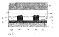
- Fig. 5c shows a carrier 71, eight layers 72 to 79 and a plurality of surface areas 79a and 79b.
- the layer 72 is a protective lacquer and / or release layer.
- the layer 73 is a replication layer.
- the layer 74 is an absorption layer.
- the layers 76 and 77 are spare layers.
- the layer 79 is an adhesive layer.
- the layers 72, 73, 74, 75, 78 and 79 are configured as described in the embodiments of FIGS. 3 and 4 and are applied to the carrier 71 as described there.
- the layer 73 consists of a replication varnish or of a thermoformable plastic.
- the layer 73 is provided with a diffractive structure as described in the description of FIG. 5a and with the layer 77 in the surface regions 79a.
- the layers 77 and 76 are both metal layers.
- the metal layer 77 is applied and provided with a diffractive structure.
- the skillful choice of material for the spacer layer 75 can be achieved by having metallic properties in the surface regions 79b. Subsequently, the metal layer 79 is applied over the entire surface.
- the 6a shows a carrier 81, seven layers 82 to 89 and a plurality of surface regions 89a and 89b.
- the layer 82 is a protective lacquer and / or release layer.
- the layer 83 is a replication layer. This layer could also be omitted here.
- the layer 84 is an absorption layer.
- the layer 86 is an equivalent layer.
- the layer 88 is a metal layer.
- the layer 89 is an adhesive layer.
- the layers 82, 83, 84, 85, 88 and 89 are designed as described in the exemplary embodiments according to FIGS. 3 and 4 and are applied to the carrier 81 as described there.
- the replacement layer 86 is formed by a transmissive material. This material may also be the same material as the material used for the spacer layer 85. As a result, as already described in the description of FIG. 5 a, a partial application of the layers 85 and 86 is dispensed with.
- FIG. 6b shows a carrier 91, seven layers 92, 93, 94, 95, 96, 98 and 99, diffractive structures 97 and a plurality of surface regions 99a to 99d.
- the layer 92 is a resist and / or release layer.
- the layer 93 is a replication layer.
- the layer 94 is an absorption layer.
- the layer 96 is an equivalent layer.
- the layer 98 is a metal layer.
- the layer 99 is an adhesive layer.
- the layers 92, 93, 94, 95, 98 and 99 are configured as described in the embodiments according to FIGS. 3 and 4 and are applied to the carrier 81 as described there.
- the replacement layer 96 is is.stallt as shown in Fig. 6a.
- the diffractive structures 97 are applied to the surface of the layer 93 by means of an embossing tool or one of the other methods described above. As can be seen from FIG. 6b, the diffractive structures 97 can in this case be applied both in surface areas which are covered by the partial thin-film element and also in areas which are not covered by a partial thin-film element.
- FIGS. 7 and 8 Several possibilities are shown in FIGS. 7 and 8 for combining a partial thin-film element with partial diffractive structures and partial metallization.
- FIG. 7 shows a carrier 101, nine layers 102 to 109 and a plurality of surface regions 109a to 109d.
- the layer 102 is a protective lacquer and / or release layer.
- the layer 103 is a replication layer.
- the layer 104 is an absorption layer.
- the layers 106, 107 and 107a are spare layers.
- the layer 108 is a metal layer.
- the layer 109 is an adhesive layer.
- the layers 102, 103, 104, 105, 108 and 109 are configured as described for FIGS. 3 and 4 and are applied to the carrier 101 as described there.
- the replacement layer 107 is a metal layer which can be constructed as described in the exemplary embodiments to FIGS. 5a and 5b.
- the replacement layers 106 and 107a are formed by a transmissive material. They are constructed as described in the embodiments of Figs. 6a and 6b.
- a diffractive structure is further applied to the layer 103 in the surface regions 109b, 109d and 109e.
- FIG. 8 shows a carrier 111, eight layers 112 to 119 and a plurality of surface regions 119a and 119b.
- the layer 112 is a resist and / or release layer.
- the layer 113 is a replication layer.
- the layer 114 is an absorption layer.
- the layer 117 is a spacer layer.
- the layers 116 and 115 are spare layers.
- the layer 118 is a metal layer.
- the layer 119 is an adhesive layer.
- the layers 112, 113, 114, 117, 118 and 119 are configured as described in the exemplary embodiments according to FIGS. 3 and 4 and are applied to the carrier 111 as described there.
- the replacement layer 115 is a metal layer that can be constructed as described in the embodiments of FIGS. 5a and 5b.
- the replacement layer 116 is formed by an etch resist (see also description of the embodiment of FIG. 3).
- a diffractive structure 115a or 114a is further applied to the layer 113 in the area regions 119c and 119d.
- individual elements fitted in, such as a partial thin-film element, a partial structuring (eg diffractive structures), a partial metallization and a partial transparent window can be produced in a positioning accuracy of up to 0.2 mm in each spatial combination as continuous or running image patterns become.
Landscapes
- Business, Economics & Management (AREA)
- Accounting & Taxation (AREA)
- Finance (AREA)
- Health & Medical Sciences (AREA)
- General Health & Medical Sciences (AREA)
- Toxicology (AREA)
- Physics & Mathematics (AREA)
- General Physics & Mathematics (AREA)
- Credit Cards Or The Like (AREA)
- Diffracting Gratings Or Hologram Optical Elements (AREA)
- Optical Modulation, Optical Deflection, Nonlinear Optics, Optical Demodulation, Optical Logic Elements (AREA)
- Laminated Bodies (AREA)
- Polarising Elements (AREA)
- Devices For Indicating Variable Information By Combining Individual Elements (AREA)
- Electrochromic Elements, Electrophoresis, Or Variable Reflection Or Absorption Elements (AREA)
Claims (23)
- Elément optiquement variable, en particulier élément de protection optiquement variable destiné à protéger des billets de banque, des cartes de crédit, ou similaires, l'élément optiquement variable présentant un film mince destiné à produire un changement de couleur au moyen d'une interférence, et une autre couche,
caractérisé en ce
que le film mince est conçu comme un élément partiel constitué d'un film mince qui ne recouvre la zone de surface de l'autre couche que sur certaines zones et comme un patron. - Elément optiquement variable selon la revendication 1,
caractérisé en ce
que l'élément partiel constitué d'un film mince présente une couche d'absorption et une couche d'espacement. - Elément optiquement variable selon la revendication 1,
caractérisé en ce
que l'élément partiel constitué d'un film mince présente plusieurs couches de réfraction distinctes. - Elément optiquement variable selon la revendication 1,
caractérisé en ce
que l'élément partiel constitué d'un film mince présente une couche réfléchissante, de préférence une couche métallique. - Elément optiquement variable selon la revendication 1,
caractérisé en ce
que l'élément partiel constitué d'un film mince présente une structure diffractive, destinée en particulier à produire des effets de diffraction. - Elément optiquement variable selon la revendication 1 ou la revendication 5,
caractérisé en ce
que l'élément partiel constitué d'un film mince présente une couche réfléchissante partielle, en particulier une couche métallique, qui ne recouvre que partiellement la zone de surface de l'élément partiel constitué d'un film mince. - Elément optiquement variable selon la revendication 1, la revendication 4 ou la revendication 6,
caractérisé en ce
que l'élément partiel constitué d'un film mince présente une structure diffractive partielle, destinée en particulier à produire des effets de diffraction, laquelle ne recouvre que partiellement la zone de surface de l'élément partiel constitué d'un film mince. - Elément optiquement variable selon l'une quelconque des revendications précédentes,
caractérisé en ce
qu'une zone de surface délimitée par l'élément partiel constitué d'un film mince de l'élément optiquement variable présente une couche d'absorption, mais pas de couche d'espacement. - Elément optiquement variable selon l'une quelconque des revendications précédentes,
caractérisé en ce
qu'une zone de surface délimitée par l'élément partiel constitué d'un film mince de l'élément optiquement variable présente une couche d'espacement, mais pas de couche d'absorption. - Elément optiquement variable selon l'une quelconque des revendications 1 à 7,
caractérisé en ce
qu'une zone de surface délimitée par l'élément partiel constitué d'un film mince présente une ou plusieurs couches de remplacement qui remplacent la succession de films minces de l'élément partiel constitué d'un film mince dans cette zone de surface. - Elément optiquement variable selon la revendication 10,
caractérisé en ce
que la zone délimitée par l'élément partiel constitué d'un film mince est entourée par l'élément partiel constitué d'un film mince ou entoure l'élément partiel constitué d'un film mince. - Elément optiquement variable selon la revendication 10,
caractérisé en ce
que l'une ou plusieurs couches de remplacement présentent une épaisseur de couche totale qui correspond à peu près à l'épaisseur de couche de l'élément partiel constitué d'un film mince. - Elément optiquement variable selon la revendication 10,
caractérisé en ce que l'une ou plusieurs couches de remplacement présentent une structure diffractive, destinée en particulier à produire des effets de diffraction. - Elément optiquement variable selon la revendication 10 ou la revendication 13,
caractérisé en ce
que l'une ou plusieurs couches de remplacement sont formées d'une couche de réflexion, en particulier d'une couche métallique, et d'une couche de support. - Elément optiquement variable selon la revendication 10 ou la revendication 13,
caractérisé en ce
que l'une ou plusieurs couches de remplacement sont formées d'une unique couche de réflexion, en particulier d'une couche métallique. - Elément optiquement variable selon la revendication 10 ou la revendication 13,
caractérisé en ce
que l'une ou plusieurs couches de remplacement sont formées d'une ou plusieurs couches transparentes. - Elément optiquement variable selon la revendication 10 ou la revendication 13,
caractérisé en ce
que l'une ou plusieurs couches de remplacement présentent une couche partiellement réfléchissante, en particulier une couche métallique, qui ne recouvre que partiellement la zone de surface de l'une ou de plusieurs couches de remplacement. - Elément optiquement variable selon la revendication 10 ou la revendication 17,
caractérisé en ce
que l'une ou plusieurs couches de remplacement présentent une structure diffractive partielle, destinée en particulier à produire des effets de diffraction, laquelle ne recouvre que partiellement la zone de surface de l'une ou de plusieurs couches de remplacement. - Elément optiquement variable selon la revendication 1,
caractérisé en ce
que l'autre couche est une couche transparente sur toute la surface, en particulier une couche de vernis de protection. - Elément optiquement variable selon la revendication 1,
caractérisé en ce
que l'autre couche est une couche réflectrice sur toute la surface, en particulier une couche métallique. - Elément optiquement variable selon la revendication 1,
caractérisé en ce
que l'autre couche est une couche adhésive sur toute la surface. - Produit de protection comportant un élément optiquement variable selon l'une quelconque des revendications précédentes.
- Feuille, en particulier feuille à marquer ou feuille à laminer, comportant un élément optiquement variable selon l'une quelconque des revendications 1 à 21.
Priority Applications (1)
| Application Number | Priority Date | Filing Date | Title |
|---|---|---|---|
| EP03718769A EP1503907B1 (fr) | 2002-05-14 | 2003-04-17 | Element optiquement variable comportant une serie de couches constituees d'un film mince |
Applications Claiming Priority (4)
| Application Number | Priority Date | Filing Date | Title |
|---|---|---|---|
| EP02010745 | 2002-05-14 | ||
| EP02010745 | 2002-05-14 | ||
| EP03718769A EP1503907B1 (fr) | 2002-05-14 | 2003-04-17 | Element optiquement variable comportant une serie de couches constituees d'un film mince |
| PCT/EP2003/004023 WO2003095228A1 (fr) | 2002-05-14 | 2003-04-17 | Element optiquement variable comportant une serie de couches constituees d'un film mince |
Publications (2)
| Publication Number | Publication Date |
|---|---|
| EP1503907A1 EP1503907A1 (fr) | 2005-02-09 |
| EP1503907B1 true EP1503907B1 (fr) | 2007-01-24 |
Family
ID=29414683
Family Applications (1)
| Application Number | Title | Priority Date | Filing Date |
|---|---|---|---|
| EP03718769A Expired - Lifetime EP1503907B1 (fr) | 2002-05-14 | 2003-04-17 | Element optiquement variable comportant une serie de couches constituees d'un film mince |
Country Status (12)
| Country | Link |
|---|---|
| US (1) | US6982832B2 (fr) |
| EP (1) | EP1503907B1 (fr) |
| JP (1) | JP4660187B2 (fr) |
| KR (1) | KR100587984B1 (fr) |
| CN (1) | CN100534806C (fr) |
| AT (1) | ATE352430T1 (fr) |
| AU (1) | AU2003222822A1 (fr) |
| DE (1) | DE50306381D1 (fr) |
| ES (1) | ES2279944T3 (fr) |
| PL (1) | PL208667B1 (fr) |
| RU (1) | RU2309050C2 (fr) |
| WO (1) | WO2003095228A1 (fr) |
Cited By (5)
| Publication number | Priority date | Publication date | Assignee | Title |
|---|---|---|---|---|
| US8613471B2 (en) | 2007-12-20 | 2013-12-24 | Giesecke & Devrient Gmbh | Security element and method for the production thereof |
| US8733797B2 (en) | 2007-12-20 | 2014-05-27 | Giesecke & Devrient Gmbh | Security element and method for the production thereof |
| US8794674B2 (en) | 2008-03-07 | 2014-08-05 | Giesecke & Devrient Gmbh | Security element and method for the production thereof |
| US9007669B2 (en) | 2008-02-15 | 2015-04-14 | Giesecke & Devrient Gmbh | Security element and method for producing the same |
| EP3726506B1 (fr) | 2019-04-19 | 2022-10-26 | Securikett Ulrich & Horn GmbH | Feuille de scellement |
Families Citing this family (33)
| Publication number | Priority date | Publication date | Assignee | Title |
|---|---|---|---|---|
| CN101164797B (zh) | 2003-07-14 | 2012-07-18 | Jds尤尼费斯公司 | 防伪线 |
| DE102004003984A1 (de) † | 2004-01-26 | 2005-08-11 | Giesecke & Devrient Gmbh | Gitterbild mit einem oder mehreren Gitterfeldern |
| AT501989B1 (de) | 2004-03-26 | 2010-04-15 | Hueck Folien Gmbh | Sicherheitsmerkmal mit unter einem bestimmten betrachtungswinkel optisch erkennbaren merkmalen |
| DE102004016596B4 (de) * | 2004-04-03 | 2006-07-27 | Ovd Kinegram Ag | Sicherheitselement in Form eines mehrschichtigen Folienkörpers und Verfahren zur Herstellung eines Sicherheitselements |
| EP1602508A1 (fr) * | 2004-06-04 | 2005-12-07 | Axalto SA | Procédé et appareil pour fabriquer un dispositif comme un hologramme, fixé sur un objet |
| DE102004042136B4 (de) * | 2004-08-30 | 2006-11-09 | Ovd Kinegram Ag | Metallisiertes Sicherheitselement |
| EP1652688A1 (fr) * | 2004-10-29 | 2006-05-03 | Arjowiggins Security | Dispositif de sécurité |
| DE102005006074B4 (de) * | 2005-02-10 | 2009-12-10 | Leonhard Kurz Gmbh & Co. Kg | Dekorierter Spritzgussartikel und Verfahren zur Herstellung des dekorierten Spritzgussartikels |
| DE102005049891A1 (de) * | 2005-10-17 | 2007-04-19 | Leonhard Kurz Gmbh & Co. Kg | Metallisierter Mehrschichtkörper |
| DE102006037431A1 (de) * | 2006-08-09 | 2008-04-17 | Ovd Kinegram Ag | Verfahren zur Herstellung eines Mehrschichtkörpers sowie Mehrschichtkörper |
| RU2415026C2 (ru) * | 2006-08-09 | 2011-03-27 | Овд Кинеграм Аг | Способ изготовления многослойного тела и многослойное тело |
| JP2008134586A (ja) * | 2006-10-23 | 2008-06-12 | Toppan Printing Co Ltd | 表示素子および表示体 |
| JP2008275740A (ja) * | 2007-04-26 | 2008-11-13 | Toppan Printing Co Ltd | 表示体及び積層体 |
| DE102007034716A1 (de) † | 2007-07-23 | 2009-01-29 | Giesecke & Devrient Gmbh | Sicherheitselement |
| FR2921584A1 (fr) | 2007-09-28 | 2009-04-03 | Oberthur Card Syst Sa | Documents securises, procedes et dispositifs d'authentification de tels documents et procede de fabrication de tels documents. |
| DE102008013073B4 (de) | 2008-03-06 | 2011-02-03 | Leonhard Kurz Stiftung & Co. Kg | Verfahren zur Herstellung eines Folienelements und Folienelement |
| DE102008017652A1 (de) * | 2008-04-04 | 2009-10-08 | Leonhard Kurz Stiftung & Co. Kg | Sicherheitselement sowie Verfahren zur Herstellung eines Sicherheitselements |
| DE102008024147B4 (de) * | 2008-05-19 | 2020-12-03 | Ovd Kinegram Ag | Optisches Sicherheitselement |
| DE102008028187A1 (de) * | 2008-06-12 | 2009-12-17 | Giesecke & Devrient Gmbh | Sicherheitselement mit optisch variablem Element. |
| DE102008027952A1 (de) | 2008-06-12 | 2009-12-17 | Giesecke & Devrient Gmbh | Sicherheitselement mit gerasterter Schicht aus Rasterelementen |
| DE102008030409A1 (de) † | 2008-06-27 | 2009-12-31 | Giesecke & Devrient Gmbh | Sicherheitselement mit Aussparung und Verfahren zur Herstellung desselben |
| DE102008036670B3 (de) * | 2008-08-06 | 2009-11-26 | Leonhard Kurz Stiftung & Co. Kg | Folie, Verfahren zu deren Herstellung, sowie Verwendung |
| DE102009008853A1 (de) | 2009-02-13 | 2010-08-19 | Giesecke & Devrient Gmbh | Durchsichtssicherheitselement |
| WO2012024718A1 (fr) * | 2010-08-23 | 2012-03-01 | Securency International Pty Ltd | Dispositif multicanal optiquement variable |
| FR2993204B1 (fr) * | 2012-07-16 | 2018-02-02 | Oberthur Fiduciaire Sas | Structure de securite. |
| GB201400910D0 (en) * | 2014-01-20 | 2014-03-05 | Rue De Int Ltd | Security elements and methods of their manufacture |
| US9857544B2 (en) * | 2015-10-09 | 2018-01-02 | Te Connectivity Nederland B.V. | Carrier having ablation-susceptible and ablation-insusceptible materials |
| KR101966851B1 (ko) * | 2017-03-06 | 2019-04-08 | 주식회사 엘지화학 | 장식 부재 및 이의 제조방법 |
| EP3594015A4 (fr) | 2017-03-06 | 2020-07-08 | LG Chem, Ltd. | Élément de décoration et procédé de fabrication d'élément de décoration |
| DE102018003030A1 (de) * | 2018-04-13 | 2019-10-17 | Giesecke+Devrient Currency Technology Gmbh | Sicherheitselement, Verfahren zum Herstellen desselben und mit dem Sicherheitselement ausgestatteter Datenträger |
| EP3650240A1 (fr) * | 2018-11-09 | 2020-05-13 | Gemalto AG | Image à couleurs multiples |
| CN111098617A (zh) * | 2020-01-09 | 2020-05-05 | 武汉红金龙印务股份有限公司 | 一种潜影压纹防伪结构及其制备工艺 |
| JP7494591B2 (ja) | 2020-06-16 | 2024-06-04 | Toppanホールディングス株式会社 | 表示体 |
Family Cites Families (7)
| Publication number | Priority date | Publication date | Assignee | Title |
|---|---|---|---|---|
| DE2545799A1 (de) * | 1975-10-13 | 1977-04-21 | Unitec Gmbh & Co Kg | Indentitaetstraeger und lesegeraet |
| US4184700A (en) * | 1975-11-17 | 1980-01-22 | Lgz Landis & Gyr Zug Ag | Documents embossed with optical markings representing genuineness information |
| DE3932505C2 (de) * | 1989-09-28 | 2001-03-15 | Gao Ges Automation Org | Datenträger mit einem optisch variablen Element |
| JPH08118857A (ja) * | 1994-10-28 | 1996-05-14 | Dainippon Printing Co Ltd | 情報記録媒体の偽造・改ざん防止方法、及び偽造・改ざん防止が図られた情報記録媒体、並びに転写シート |
| JPH09254520A (ja) * | 1996-03-26 | 1997-09-30 | Dainippon Printing Co Ltd | 色変化するカード |
| US6761959B1 (en) | 1999-07-08 | 2004-07-13 | Flex Products, Inc. | Diffractive surfaces with color shifting backgrounds |
| GB0015873D0 (en) * | 2000-06-28 | 2000-08-23 | Rue De Int Ltd | Optically variable security device |
-
2003
- 2003-04-17 AU AU2003222822A patent/AU2003222822A1/en not_active Abandoned
- 2003-04-17 WO PCT/EP2003/004023 patent/WO2003095228A1/fr active IP Right Grant
- 2003-04-17 KR KR1020047018251A patent/KR100587984B1/ko not_active IP Right Cessation
- 2003-04-17 DE DE50306381T patent/DE50306381D1/de not_active Expired - Lifetime
- 2003-04-17 AT AT03718769T patent/ATE352430T1/de active
- 2003-04-17 PL PL373142A patent/PL208667B1/pl unknown
- 2003-04-17 RU RU2004136320/12A patent/RU2309050C2/ru not_active IP Right Cessation
- 2003-04-17 ES ES03718769T patent/ES2279944T3/es not_active Expired - Lifetime
- 2003-04-17 EP EP03718769A patent/EP1503907B1/fr not_active Expired - Lifetime
- 2003-04-17 JP JP2004503282A patent/JP4660187B2/ja not_active Expired - Fee Related
- 2003-04-17 US US10/513,521 patent/US6982832B2/en not_active Expired - Lifetime
- 2003-04-17 CN CNB038107724A patent/CN100534806C/zh not_active Expired - Fee Related
Cited By (5)
| Publication number | Priority date | Publication date | Assignee | Title |
|---|---|---|---|---|
| US8613471B2 (en) | 2007-12-20 | 2013-12-24 | Giesecke & Devrient Gmbh | Security element and method for the production thereof |
| US8733797B2 (en) | 2007-12-20 | 2014-05-27 | Giesecke & Devrient Gmbh | Security element and method for the production thereof |
| US9007669B2 (en) | 2008-02-15 | 2015-04-14 | Giesecke & Devrient Gmbh | Security element and method for producing the same |
| US8794674B2 (en) | 2008-03-07 | 2014-08-05 | Giesecke & Devrient Gmbh | Security element and method for the production thereof |
| EP3726506B1 (fr) | 2019-04-19 | 2022-10-26 | Securikett Ulrich & Horn GmbH | Feuille de scellement |
Also Published As
| Publication number | Publication date |
|---|---|
| RU2004136320A (ru) | 2005-05-27 |
| KR20050007537A (ko) | 2005-01-19 |
| US6982832B2 (en) | 2006-01-03 |
| DE50306381D1 (de) | 2007-03-15 |
| CN1652946A (zh) | 2005-08-10 |
| JP2006504545A (ja) | 2006-02-09 |
| US20050141094A1 (en) | 2005-06-30 |
| JP4660187B2 (ja) | 2011-03-30 |
| ES2279944T3 (es) | 2007-09-01 |
| CN100534806C (zh) | 2009-09-02 |
| RU2309050C2 (ru) | 2007-10-27 |
| PL373142A1 (en) | 2005-08-22 |
| EP1503907A1 (fr) | 2005-02-09 |
| ATE352430T1 (de) | 2007-02-15 |
| PL208667B1 (pl) | 2011-05-31 |
| KR100587984B1 (ko) | 2006-06-08 |
| WO2003095228A1 (fr) | 2003-11-20 |
| AU2003222822A1 (en) | 2003-11-11 |
Similar Documents
| Publication | Publication Date | Title |
|---|---|---|
| EP1503907B1 (fr) | Element optiquement variable comportant une serie de couches constituees d'un film mince | |
| EP1503906B1 (fr) | Element optiquement variable comportant un element partiel transparent | |
| EP1476315B1 (fr) | Element de securite et document de securite pourvu d'un tel element de securite | |
| DE10232245B4 (de) | Optisch variables Element mit variierender Distanzschicht-Dicke | |
| EP1478520B1 (fr) | Document securise et element de securite pour un document securise | |
| EP1800271B1 (fr) | Document de securite | |
| EP2114673B1 (fr) | Document de sécurité | |
| EP1747100B1 (fr) | Element de securite se presentant sous la forme d'un corps en pellicule multicouche | |
| EP1713645B2 (fr) | Grille-image comprenant plusieurs champs de grille | |
| EP2117840B1 (fr) | Élément de sécurité pour un document protégé et procédé de fabrication de l'élément de sécurité | |
| EP2173571A2 (fr) | Élément de sécurité | |
| DE10202035A1 (de) | Sicherheitselement mit Farbkippeffekt und magnetischen Eigenschaften, Gegenstand mit einem solchen Sicherheitselement sowie Verfahren zur Herstellung des Sicherheitselements und des Gegenstands. | |
| DE102015010945A1 (de) | Wertdokument | |
| DE102008049513A1 (de) | Gitterbild mit achromatischen Gitterfeldern | |
| DE102014200595B4 (de) | Sicherheitsanordnung sowie Verfahren zur Herstellung einer Sicherheitsanordnung |
Legal Events
| Date | Code | Title | Description |
|---|---|---|---|
| PUAI | Public reference made under article 153(3) epc to a published international application that has entered the european phase |
Free format text: ORIGINAL CODE: 0009012 |
|
| 17P | Request for examination filed |
Effective date: 20041021 |
|
| AK | Designated contracting states |
Kind code of ref document: A1 Designated state(s): AT BE BG CH CY CZ DE DK EE ES FI FR GB GR HU IE IT LI LU MC NL PT RO SE SI SK TR |
|
| AX | Request for extension of the european patent |
Extension state: AL LT LV MK |
|
| DAX | Request for extension of the european patent (deleted) | ||
| GRAP | Despatch of communication of intention to grant a patent |
Free format text: ORIGINAL CODE: EPIDOSNIGR1 |
|
| GRAS | Grant fee paid |
Free format text: ORIGINAL CODE: EPIDOSNIGR3 |
|
| GRAA | (expected) grant |
Free format text: ORIGINAL CODE: 0009210 |
|
| AK | Designated contracting states |
Kind code of ref document: B1 Designated state(s): AT BE BG CH CY CZ DE DK EE ES FI FR GB GR HU IE IT LI LU MC NL PT RO SE SI SK TR |
|
| PG25 | Lapsed in a contracting state [announced via postgrant information from national office to epo] |
Ref country code: FI Free format text: LAPSE BECAUSE OF FAILURE TO SUBMIT A TRANSLATION OF THE DESCRIPTION OR TO PAY THE FEE WITHIN THE PRESCRIBED TIME-LIMIT Effective date: 20070124 Ref country code: DK Free format text: LAPSE BECAUSE OF FAILURE TO SUBMIT A TRANSLATION OF THE DESCRIPTION OR TO PAY THE FEE WITHIN THE PRESCRIBED TIME-LIMIT Effective date: 20070124 Ref country code: SI Free format text: LAPSE BECAUSE OF FAILURE TO SUBMIT A TRANSLATION OF THE DESCRIPTION OR TO PAY THE FEE WITHIN THE PRESCRIBED TIME-LIMIT Effective date: 20070124 |
|
| REG | Reference to a national code |
Ref country code: GB Ref legal event code: FG4D Free format text: NOT ENGLISH |
|
| REG | Reference to a national code |
Ref country code: CH Ref legal event code: EP |
|
| REG | Reference to a national code |
Ref country code: IE Ref legal event code: FG4D Free format text: LANGUAGE OF EP DOCUMENT: GERMAN |
|
| REF | Corresponds to: |
Ref document number: 50306381 Country of ref document: DE Date of ref document: 20070315 Kind code of ref document: P |
|
| REG | Reference to a national code |
Ref country code: SE Ref legal event code: TRGR |
|
| PG25 | Lapsed in a contracting state [announced via postgrant information from national office to epo] |
Ref country code: BG Free format text: LAPSE BECAUSE OF EXPIRATION OF PROTECTION Effective date: 20070425 |
|
| REG | Reference to a national code |
Ref country code: CH Ref legal event code: NV Representative=s name: FIAMMENGHI-FIAMMENGHI |
|
| GBT | Gb: translation of ep patent filed (gb section 77(6)(a)/1977) |
Effective date: 20070410 |
|
| PG25 | Lapsed in a contracting state [announced via postgrant information from national office to epo] |
Ref country code: PT Free format text: LAPSE BECAUSE OF FAILURE TO SUBMIT A TRANSLATION OF THE DESCRIPTION OR TO PAY THE FEE WITHIN THE PRESCRIBED TIME-LIMIT Effective date: 20070625 |
|
| ET | Fr: translation filed | ||
| REG | Reference to a national code |
Ref country code: ES Ref legal event code: FG2A Ref document number: 2279944 Country of ref document: ES Kind code of ref document: T3 |
|
| PLBI | Opposition filed |
Free format text: ORIGINAL CODE: 0009260 |
|
| PLAX | Notice of opposition and request to file observation + time limit sent |
Free format text: ORIGINAL CODE: EPIDOSNOBS2 |
|
| PG25 | Lapsed in a contracting state [announced via postgrant information from national office to epo] |
Ref country code: SK Free format text: LAPSE BECAUSE OF FAILURE TO SUBMIT A TRANSLATION OF THE DESCRIPTION OR TO PAY THE FEE WITHIN THE PRESCRIBED TIME-LIMIT Effective date: 20070124 |
|
| 26 | Opposition filed |
Opponent name: DE LA RUE INTERNATIONAL LIMITED Effective date: 20071019 |
|
| PG25 | Lapsed in a contracting state [announced via postgrant information from national office to epo] |
Ref country code: RO Free format text: LAPSE BECAUSE OF FAILURE TO SUBMIT A TRANSLATION OF THE DESCRIPTION OR TO PAY THE FEE WITHIN THE PRESCRIBED TIME-LIMIT Effective date: 20070124 |
|
| NLR1 | Nl: opposition has been filed with the epo |
Opponent name: DE LA RUE INTERNATIONAL LIMITED |
|
| PLAF | Information modified related to communication of a notice of opposition and request to file observations + time limit |
Free format text: ORIGINAL CODE: EPIDOSCOBS2 |
|
| PG25 | Lapsed in a contracting state [announced via postgrant information from national office to epo] |
Ref country code: GR Free format text: LAPSE BECAUSE OF FAILURE TO SUBMIT A TRANSLATION OF THE DESCRIPTION OR TO PAY THE FEE WITHIN THE PRESCRIBED TIME-LIMIT Effective date: 20070425 |
|
| PLAF | Information modified related to communication of a notice of opposition and request to file observations + time limit |
Free format text: ORIGINAL CODE: EPIDOSCOBS2 |
|
| PLBP | Opposition withdrawn |
Free format text: ORIGINAL CODE: 0009264 |
|
| PG25 | Lapsed in a contracting state [announced via postgrant information from national office to epo] |
Ref country code: EE Free format text: LAPSE BECAUSE OF FAILURE TO SUBMIT A TRANSLATION OF THE DESCRIPTION OR TO PAY THE FEE WITHIN THE PRESCRIBED TIME-LIMIT Effective date: 20070124 |
|
| PG25 | Lapsed in a contracting state [announced via postgrant information from national office to epo] |
Ref country code: MC Free format text: LAPSE BECAUSE OF NON-PAYMENT OF DUE FEES Effective date: 20070430 |
|
| PG25 | Lapsed in a contracting state [announced via postgrant information from national office to epo] |
Ref country code: CY Free format text: LAPSE BECAUSE OF FAILURE TO SUBMIT A TRANSLATION OF THE DESCRIPTION OR TO PAY THE FEE WITHIN THE PRESCRIBED TIME-LIMIT Effective date: 20070124 |
|
| PG25 | Lapsed in a contracting state [announced via postgrant information from national office to epo] |
Ref country code: LU Free format text: LAPSE BECAUSE OF NON-PAYMENT OF DUE FEES Effective date: 20070417 |
|
| PLBD | Termination of opposition procedure: decision despatched |
Free format text: ORIGINAL CODE: EPIDOSNOPC1 |
|
| PG25 | Lapsed in a contracting state [announced via postgrant information from national office to epo] |
Ref country code: HU Free format text: LAPSE BECAUSE OF FAILURE TO SUBMIT A TRANSLATION OF THE DESCRIPTION OR TO PAY THE FEE WITHIN THE PRESCRIBED TIME-LIMIT Effective date: 20070725 Ref country code: TR Free format text: LAPSE BECAUSE OF FAILURE TO SUBMIT A TRANSLATION OF THE DESCRIPTION OR TO PAY THE FEE WITHIN THE PRESCRIBED TIME-LIMIT Effective date: 20070124 |
|
| PLBM | Termination of opposition procedure: date of legal effect published |
Free format text: ORIGINAL CODE: 0009276 |
|
| STAA | Information on the status of an ep patent application or granted ep patent |
Free format text: STATUS: OPPOSITION PROCEDURE CLOSED |
|
| 27C | Opposition proceedings terminated |
Effective date: 20091015 |
|
| REG | Reference to a national code |
Ref country code: FR Ref legal event code: PLFP Year of fee payment: 14 |
|
| REG | Reference to a national code |
Ref country code: FR Ref legal event code: PLFP Year of fee payment: 15 |
|
| REG | Reference to a national code |
Ref country code: FR Ref legal event code: PLFP Year of fee payment: 16 |
|
| PGFP | Annual fee paid to national office [announced via postgrant information from national office to epo] |
Ref country code: IE Payment date: 20180418 Year of fee payment: 16 Ref country code: CZ Payment date: 20180405 Year of fee payment: 16 Ref country code: ES Payment date: 20180523 Year of fee payment: 16 |
|
| PGFP | Annual fee paid to national office [announced via postgrant information from national office to epo] |
Ref country code: BE Payment date: 20180423 Year of fee payment: 16 |
|
| REG | Reference to a national code |
Ref country code: BE Ref legal event code: MM Effective date: 20190430 |
|
| PG25 | Lapsed in a contracting state [announced via postgrant information from national office to epo] |
Ref country code: CZ Free format text: LAPSE BECAUSE OF NON-PAYMENT OF DUE FEES Effective date: 20190417 |
|
| PG25 | Lapsed in a contracting state [announced via postgrant information from national office to epo] |
Ref country code: BE Free format text: LAPSE BECAUSE OF NON-PAYMENT OF DUE FEES Effective date: 20190430 |
|
| PG25 | Lapsed in a contracting state [announced via postgrant information from national office to epo] |
Ref country code: IE Free format text: LAPSE BECAUSE OF NON-PAYMENT OF DUE FEES Effective date: 20190417 |
|
| REG | Reference to a national code |
Ref country code: ES Ref legal event code: FD2A Effective date: 20200901 |
|
| PG25 | Lapsed in a contracting state [announced via postgrant information from national office to epo] |
Ref country code: ES Free format text: LAPSE BECAUSE OF NON-PAYMENT OF DUE FEES Effective date: 20190418 |
|
| PGFP | Annual fee paid to national office [announced via postgrant information from national office to epo] |
Ref country code: IT Payment date: 20210430 Year of fee payment: 19 Ref country code: FR Payment date: 20210421 Year of fee payment: 19 Ref country code: DE Payment date: 20210414 Year of fee payment: 19 |
|
| PGFP | Annual fee paid to national office [announced via postgrant information from national office to epo] |
Ref country code: CH Payment date: 20210422 Year of fee payment: 19 Ref country code: GB Payment date: 20210422 Year of fee payment: 19 Ref country code: SE Payment date: 20210420 Year of fee payment: 19 Ref country code: AT Payment date: 20210420 Year of fee payment: 19 |
|
| PGFP | Annual fee paid to national office [announced via postgrant information from national office to epo] |
Ref country code: NL Payment date: 20210421 Year of fee payment: 19 |
|
| REG | Reference to a national code |
Ref country code: DE Ref legal event code: R119 Ref document number: 50306381 Country of ref document: DE |
|
| REG | Reference to a national code |
Ref country code: SE Ref legal event code: EUG |
|
| REG | Reference to a national code |
Ref country code: CH Ref legal event code: PL |
|
| REG | Reference to a national code |
Ref country code: NL Ref legal event code: MM Effective date: 20220501 |
|
| REG | Reference to a national code |
Ref country code: AT Ref legal event code: MM01 Ref document number: 352430 Country of ref document: AT Kind code of ref document: T Effective date: 20220417 |
|
| GBPC | Gb: european patent ceased through non-payment of renewal fee |
Effective date: 20220417 |
|
| PG25 | Lapsed in a contracting state [announced via postgrant information from national office to epo] |
Ref country code: SE Free format text: LAPSE BECAUSE OF NON-PAYMENT OF DUE FEES Effective date: 20220418 Ref country code: NL Free format text: LAPSE BECAUSE OF NON-PAYMENT OF DUE FEES Effective date: 20220501 Ref country code: LI Free format text: LAPSE BECAUSE OF NON-PAYMENT OF DUE FEES Effective date: 20220430 Ref country code: GB Free format text: LAPSE BECAUSE OF NON-PAYMENT OF DUE FEES Effective date: 20220417 Ref country code: FR Free format text: LAPSE BECAUSE OF NON-PAYMENT OF DUE FEES Effective date: 20220430 Ref country code: DE Free format text: LAPSE BECAUSE OF NON-PAYMENT OF DUE FEES Effective date: 20221103 Ref country code: CH Free format text: LAPSE BECAUSE OF NON-PAYMENT OF DUE FEES Effective date: 20220430 Ref country code: AT Free format text: LAPSE BECAUSE OF NON-PAYMENT OF DUE FEES Effective date: 20220417 |
|
| PG25 | Lapsed in a contracting state [announced via postgrant information from national office to epo] |
Ref country code: IT Free format text: LAPSE BECAUSE OF NON-PAYMENT OF DUE FEES Effective date: 20220417 |