EP1503618A2 - Elektronische Vorrichtung - Google Patents
Elektronische Vorrichtung Download PDFInfo
- Publication number
- EP1503618A2 EP1503618A2 EP04254499A EP04254499A EP1503618A2 EP 1503618 A2 EP1503618 A2 EP 1503618A2 EP 04254499 A EP04254499 A EP 04254499A EP 04254499 A EP04254499 A EP 04254499A EP 1503618 A2 EP1503618 A2 EP 1503618A2
- Authority
- EP
- European Patent Office
- Prior art keywords
- casing
- carbon fiber
- conductive layer
- electronic device
- exposed
- Prior art date
- Legal status (The legal status is an assumption and is not a legal conclusion. Google has not performed a legal analysis and makes no representation as to the accuracy of the status listed.)
- Withdrawn
Links
Images



Classifications
-
- H—ELECTRICITY
- H05—ELECTRIC TECHNIQUES NOT OTHERWISE PROVIDED FOR
- H05K—PRINTED CIRCUITS; CASINGS OR CONSTRUCTIONAL DETAILS OF ELECTRIC APPARATUS; MANUFACTURE OF ASSEMBLAGES OF ELECTRICAL COMPONENTS
- H05K5/00—Casings, cabinets or drawers for electric apparatus
- H05K5/02—Details
- H05K5/03—Covers
-
- H—ELECTRICITY
- H05—ELECTRIC TECHNIQUES NOT OTHERWISE PROVIDED FOR
- H05K—PRINTED CIRCUITS; CASINGS OR CONSTRUCTIONAL DETAILS OF ELECTRIC APPARATUS; MANUFACTURE OF ASSEMBLAGES OF ELECTRICAL COMPONENTS
- H05K9/00—Screening of apparatus or components against electric or magnetic fields
- H05K9/0073—Shielding materials
- H05K9/0081—Electromagnetic shielding materials, e.g. EMI, RFI shielding
- H05K9/009—Electromagnetic shielding materials, e.g. EMI, RFI shielding comprising electro-conductive fibres, e.g. metal fibres, carbon fibres, metallised textile fibres, electro-conductive mesh, woven, non-woven mat, fleece, cross-linked
-
- H—ELECTRICITY
- H01—ELECTRIC ELEMENTS
- H01B—CABLES; CONDUCTORS; INSULATORS; SELECTION OF MATERIALS FOR THEIR CONDUCTIVE, INSULATING OR DIELECTRIC PROPERTIES
- H01B1/00—Conductors or conductive bodies characterised by the conductive materials; Selection of materials as conductors
- H01B1/20—Conductive material dispersed in non-conductive organic material
- H01B1/24—Conductive material dispersed in non-conductive organic material the conductive material comprising carbon-silicon compounds, carbon or silicon
-
- H—ELECTRICITY
- H04—ELECTRIC COMMUNICATION TECHNIQUE
- H04N—PICTORIAL COMMUNICATION, e.g. TELEVISION
- H04N23/00—Cameras or camera modules comprising electronic image sensors; Control thereof
- H04N23/50—Constructional details
- H04N23/51—Housings
Definitions
- This invention relates to an electronic device using a carbon fiber reinforced resin for its casing.
- unwanted electromagnetic noise is generated from a charge couple device (CCD), which is an image pickup device, and a printed circuit board having a driving control circuit of a rotary head unit mounted thereon.
- CCD charge couple device
- the CCD and the printed circuit board are covered with shield cases made of a conductive metal, respectively, and the shield cases are grounded. Since a head amplifier for processing and amplifying minute video signals need be protected from external electromagnetic waves, it is shielded by a shield plate. However, each of these shielding measures complicates the device structure and makes its assembly difficult.
- its outer casing is made of an electromagnetic absorbing material such as ceramics or magnesium alloy so that the outer casing absorbs unwanted electromagnetic waves generated from internal electronic components and external electromagnetic waves.
- an electromagnetic absorbing material such as ceramics or magnesium alloy
- the metal casing made of magnesium alloy or the like needs secondary processing such as surface polishing and anticorrosive treatment in order to reduce roughness of the surface. Therefore, there are problems of low productivity and very high cost.
- a casing formed by injection-molding a glass fiber reinforced resin, carbon fiber reinforced resin or the like having small thickness, light weight, high strength and high rigidity is used, other than the above-described metal casing made of magnesium alloy or the like.
- the glass fiber or carbon fiber is exposed on the surface and the surface becomes rough, or the unevenness of the fibers appears clearly and the appearance of the casing is deteriorated.
- secondary processing such as surface coating and polishing is carried out, the coating is stripped off the part where the glass fiber or carbon fiber is exposed.
- the carbon fiber breaking out from the surface of the casing may contaminate the periphery and occurrence of a short circuit due to the carbon fiber exposed from the surface of the casing may be anticipated.
- an object of this invention to provide an electronic device having a casing that prevents leakage of unwanted electromagnetic waves from inside, is not affected by external electromagnetic waves, has small thickness, light weight, high strength and high rigidity, and has excellent contact property with coating.
- an electronic device has at least a casing that has an electronic component housed therein.
- the casing is made of a carbon fiber reinforced resin having a conductive layer made of a mixture of a carbon fiber and a thermoplastic resin and an insulating layer where only the thermoplastic resin is exposed on a surface of the conductive layer.
- the casing made of the carbon fiber reinforced resin absorbs unwanted electromagnetic waves generated from the internal electronic component and also absorbs external electromagnetic waves. Occurrence of noise and electromagnetic interruption can be thus prevented. Moreover, since the casing is made of the carbon fiber reinforced resin having the conductive layer made of the mixture of the carbon fiber and the thermoplastic resin and the insulating layer where only the thermoplastic resin is exposed on the surface of the conductive layer, the casing has small thickness, light weight, high strength and high rigidity, and the carbon fiber is not exposed on the surface.
- the electronic device does not have the problems of roughness of the surface of the casing and stripping of coating when it is used on the surface of the casing.
- the surface of the casing can be neatly finished.
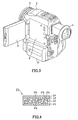
- the electronic device to which this invention is applied is a camera-integrated digital video tape recorder (hereinafter referred to as digital video camera) 1, for example, shown in Figs. 1, 2 and 3.
- digital video camera 1 has a body part 2 having a substantially rectangular solid-shape as a whole.
- an image pickup unit for picking up an image of an object
- a display unit for displaying a picked-up image
- an audio recording unit for recording sounds
- a recording/reproducing unit for recording/reproducing image signals and audio signals from the image pickup unit and the audio recording unit
- operating buttons and switches for performing various operations.
- a lens part 3 is provided at which an image pickup lens 3a is exposed.
- a view finder part 4 for a person who picks up an image to view a liquid crystal display (LCD) displaying an image picked up by an internal charge coupled device (CCD) through the image pickup lens 3a is provided in such a manner that the view finder part 4 can be pulled out.
- a holding part 6 is provided on which a grip belt 5 is attached for the person who picks up an image to hold the video camera 1.
- a cover 7 attached to be freely open and close on the holding part 6 is opened, it is found that a cassette loading part for loading a tape cassette is provided inside.
- a panel part 8 is mounted to be freely open and close.
- the panel part 8 is closed, as shown in Fig.1, the panel part 8 is housed in a panel housing part 9 formed by cutting out the lateral side of the body part 2.
- an image picked up by the image pickup lens 3a can be displayed on a liquid crystal panel (LCD) provided on a major surface of the panel part 8 facing the panel housing part 9, as well as on the above-described view finder part 4 on the rear side.
- a battery 10 as a power source is removably mounted below the panel part 8.
- the person who picks up an image can picks up an image, holding by one hand the holding part 6 provided on the one lateral side of the body part 2 and viewing the view finder part 4 on the rear side, or viewing the liquid crystal panel when with the panel part 8 provided on the other lateral side of the body part 2 is opened.
- this digital video camera 1 is characterized in that a casing 20 forming the outer casing of the above-described body part 2 and the panel part 8 is made of a carbon fiber reinforced resin (carbon fiber reinforced plastics) having a conductive layer 22 made of a mixture of a carbon fiber 21 a and a thermoplastic resin 21b and an insulating layer 23 where only the thermoplastic resin 21b is exposed on the surface of the conductive layer 22, as shown in Fig.4.
- a casing 20 forming the outer casing of the above-described body part 2 and the panel part 8 is made of a carbon fiber reinforced resin (carbon fiber reinforced plastics) having a conductive layer 22 made of a mixture of a carbon fiber 21 a and a thermoplastic resin 21b and an insulating layer 23 where only the thermoplastic resin 21b is exposed on the surface of the conductive layer 22, as shown in Fig.4.
- This casing 20 is formed by injection molding in which the temperature of the cavity surface of a metal mold is raised to a high temperature so that the carbon fiber 21a is not exposed on the surface.
- the cavity of the metal mold is filled with a carbon fiber reinforced resin material containing the carbon fiber 21a and the thermoplastic resin 21b.
- the carbon fiber 21a is sunk in the thermoplastic resin 21b.
- the casing 20 having, as its core layer, the conductor layer 22 made of the mixture of the carbon fiber 21 a and the thermoplastic resin 21b, and having, as its outer surface layer, the insulating layer 23 where only the thermoplastic resin 21b is exposed on the surface of the conductive layer 22, can be acquired. Since the temperature of the cavity surface is raised, the fluidity of the carbon fiber reinforced resin material is improved and it can be molded with a small thickness.
- the carbon fiber reinforced resin material for example, TORAYCA long fiber pellets manufactured by Toray Industries, Inc. can be used. Specifically, using a carbon fiber reinforced resin containing the carbon fiber 21a at a rate of 10 to 30% by weight of the total weight, the casing 20 in which the carbon fiber 21a is not exposed on the surface can be acquired by the above-described injection molding. More preferably, if the content of the carbon fiber 21a is 15 to 25% by weight, the casing 20 having small thickness, light weight, high strength and high rigidity can be produced. By using a long fiber having a large aspect ratio for the carbon fiber 21a, the mechanical strength and conductivity can be improved.
- thermoplastic resin 21b engineering plastics, for example, polybutylene terephthalate (PBT) resin, polyphenylene sulfide (PPS) resin, polyacetal (PA) resin, polycarbonate (PC) resin, polyethylene terephthalate (PET) resin, polyphenylene ether (PPE) resin or the like can be used.
- PBT polybutylene terephthalate
- PPS polyphenylene sulfide
- PA polyacetal
- PC polycarbonate
- PET polyethylene terephthalate
- PPE polyphenylene ether
- an ornamental layer 24 is formed by coating.
- this coating brush painting, spraying, electrostatic coating or the like is used.
- the coating material a lacquer type material, enamel type material, ultraviolet/electron-beam hardening type material or the like is used.
- this casing 20 is made of the carbon fiber reinforced resin having the conductive layer 22 made of the mixture of the carbon fiber 21a and the thermoplastic resin 21b and the insulating layer 23 where only the thermoplastic resin 21b is exposed on the surface of the conductive layer 22, the casing 20 has small thickness, light weight, high strength and high rigidity, and the carbon fiber 21a is not exposed on the surface.
- the digital video camera 1 there are no problems of roughness of the surface of the casing 20 and of stripping of the coating when the coating is applied on the surface of the casing 20.
- the surface of the casing 20 can be neatly finished, using the ornamental layer 24.
- the digital video camera 1 secondary processing such as polishing and anticorrosive treatment on the surface of the casing 20 is not necessary. Since the casing 20 has high molding property and allows a high degree of freedom in shape, the productivity can be improved significantly.
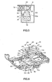
- a lens cylinder 30 in which an optical system including the image pickup lens 3a is arranged, and a CCD 31 attached on the rear side of the lens cylinder 30 and adapted for picking up an image of an object formed y the lens cylinder 30 are provided, as shown in Fig.5.
- a rotary head unit 33 for recording and reproducing signals to and from a magnetic tape 32a of a tape cassette 32 loaded in a tape cassette loading part, and a tape driving mechanism 36 for driving the magnetic tape 32 led by plural guide rollers and sandwiched between a pinch roller 34 and a capstan 35, at a constant speed.
- the CCD 31 is an electronic component that generates unwanted electromagnetic waves (unwanted radiation). Unwanted electromagnetic noise is also generated from a printed circuit board on which a driving control circuit or the like of the rotary head unit 33 is mounted.
- the head amplifier for amplifying a video signal picked up by the CCD 31 is an electronic component susceptible to external electromagnetic waves, though not shown.
- the above-described casing 20 made of the carbon fiber reinforced resin absorbs the unwanted electromagnetic waves generated from the internal electronic components and also absorbs the external electromagnetic waves. This enables prevention of occurrence noise and electromagnetic interruption and enables realization of excellent electromagnetic shielding property.
- a printed circuit board 40 On the inner surface of the casing 20, a printed circuit board 40 on which electronic components such as IC chips, connectors, passive elements and active elements are mounted, electronic components such as a driving motor, a flexible wiring board (wiring cable) 41 electrically connected with these electronic components and the printed circuit board 40, and a metal frame 42 supporting these electronic components, the printed circuit board 40 and various mechanisms are attached by screwing, for example, as shown in Figs.6 and 7.
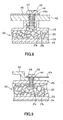
- plural bosses 43 are projected on the inner surface of the casing 20, and screw holes 44 with a depth to be exposed to the conductive layer 22 from the insulating layer 23 are formed at the centers of the bosses 43, as shown in Fig.8.
- the screw holes 44 are self-tap holes formed by screwing tap screws 45.
- the conductor patterns 46 is formed as a grounding pattern and has a land part 46a corresponding to the top part of the screw 45 on the periphery of the through-hole 47.
- the printed circuit board 40 is fixed on the inner surface of the casing 20 and the conductor pattern 46 is electrically continued to the conductive layer 22 via the screws 45.
- the screw holes 44 for screwing the above-described flexible wiring board 41 and the metal frame 42 are formed, as shown in Fig.9.
- through-holes 48 for passing the screws 45 in the direction of the thickness are formed.
- the metal frame 42 is fixed on the inner surface of the casing 20 and is electrically continued to the conductive layer 22 via the screws 45.
- a wiring part 41a to be a grounding wire is branched and extended to the positions where the metal frame 42 is fixed. As the distal end of the wiring part 41 a is screwed between the metal frame 42 and the screw 45, the flexible wiring board 41 is electrically continued to the conductive layer 22 via the metal frame 42 and the screw 45.
- This invention is not limited to the above-described digital video camera 1 and can be broadly applied to electronic devices in which electronic components generating electromagnetic waves and electronic components susceptible to external electromagnetic waves are provided within its casing. Particularly, if this invention is applied to a portable electronic device, it is possible to realize further reduction in size and weight while taking measures to prevent EMI and ESD and maintaining the mechanical strength of the casing.
Landscapes
- Engineering & Computer Science (AREA)
- Physics & Mathematics (AREA)
- Microelectronics & Electronic Packaging (AREA)
- Signal Processing (AREA)
- Chemical & Material Sciences (AREA)
- Dispersion Chemistry (AREA)
- Spectroscopy & Molecular Physics (AREA)
- Textile Engineering (AREA)
- Electromagnetism (AREA)
- Multimedia (AREA)
- Shielding Devices Or Components To Electric Or Magnetic Fields (AREA)
- Camera Bodies And Camera Details Or Accessories (AREA)
- Casings For Electric Apparatus (AREA)
- Studio Devices (AREA)
- Moulds For Moulding Plastics Or The Like (AREA)
Applications Claiming Priority (2)
| Application Number | Priority Date | Filing Date | Title |
|---|---|---|---|
| JP2003283228 | 2003-07-30 | ||
| JP2003283228A JP2005051129A (ja) | 2003-07-30 | 2003-07-30 | 電子機器 |
Publications (2)
| Publication Number | Publication Date |
|---|---|
| EP1503618A2 true EP1503618A2 (de) | 2005-02-02 |
| EP1503618A3 EP1503618A3 (de) | 2007-08-15 |
Family
ID=33535694
Family Applications (1)
| Application Number | Title | Priority Date | Filing Date |
|---|---|---|---|
| EP04254499A Withdrawn EP1503618A3 (de) | 2003-07-30 | 2004-07-28 | Elektronische Vorrichtung |
Country Status (5)
| Country | Link |
|---|---|
| US (1) | US7310236B2 (de) |
| EP (1) | EP1503618A3 (de) |
| JP (1) | JP2005051129A (de) |
| KR (1) | KR20050014660A (de) |
| CN (1) | CN100342767C (de) |
Cited By (1)
| Publication number | Priority date | Publication date | Assignee | Title |
|---|---|---|---|---|
| EP2148394A3 (de) * | 2008-07-25 | 2011-07-20 | Fujitsu Limited | Steckerstruktur, Stecker, Steckdose und elektronisches Gerät |
Families Citing this family (36)
| Publication number | Priority date | Publication date | Assignee | Title |
|---|---|---|---|---|
| EP1219401A3 (de) * | 2000-12-29 | 2004-02-04 | Nokia Corporation | Spritzgiessformteil mit einem verstärkenden oder dekoratieven Kern |
| JP4635679B2 (ja) * | 2005-03-28 | 2011-02-23 | パナソニック電工株式会社 | 電磁波シールド筐体の製造方法 |
| JP2008104037A (ja) * | 2006-10-20 | 2008-05-01 | Fujifilm Corp | 撮像装置 |
| CN101214918B (zh) * | 2007-01-04 | 2012-04-18 | 菱生精密工业股份有限公司 | 用于微机电封盖制程的封装结构 |
| JP2008191433A (ja) * | 2007-02-06 | 2008-08-21 | Fujifilm Corp | タップネジの導電構造、及び電子機器 |
| US8574696B2 (en) * | 2007-07-31 | 2013-11-05 | Hewlett-Packard Development Company, L.P. | Electronic device housing assembly |
| JP4421663B1 (ja) * | 2008-09-10 | 2010-02-24 | 株式会社東芝 | プリント配線板、電子機器 |
| JP4489133B2 (ja) * | 2008-09-10 | 2010-06-23 | 株式会社東芝 | プリント配線板、電子機器 |
| TWM361848U (en) * | 2008-12-24 | 2009-07-21 | Micro Star Int Co Ltd | Fixing mechanism capable of reducing electromagnetic radiation interference and related electronic device |
| US7845956B1 (en) * | 2009-05-26 | 2010-12-07 | Thomas Baycura | Electrical component interface |
| JP2011014239A (ja) * | 2009-06-30 | 2011-01-20 | Sanyo Electric Co Ltd | 電子機器 |
| KR101032252B1 (ko) * | 2009-10-23 | 2011-05-02 | 삼성전기주식회사 | 동화상 카메라 및 이를 포함하는 전자장치 |
| US20150222311A1 (en) * | 2012-08-27 | 2015-08-06 | Motorola Solutions ,Inc. | Housing for electrostatic discharge protection of a portable communication device |
| JP2015018936A (ja) * | 2013-07-11 | 2015-01-29 | パナソニックIpマネジメント株式会社 | 電子機器と、それを搭載した自動車 |
| JP6322951B2 (ja) * | 2013-10-18 | 2018-05-16 | 株式会社デンソー | 車両電子装置 |
| US9575560B2 (en) | 2014-06-03 | 2017-02-21 | Google Inc. | Radar-based gesture-recognition through a wearable device |
| US9921660B2 (en) | 2014-08-07 | 2018-03-20 | Google Llc | Radar-based gesture recognition |
| US9811164B2 (en) | 2014-08-07 | 2017-11-07 | Google Inc. | Radar-based gesture sensing and data transmission |
| US10268321B2 (en) | 2014-08-15 | 2019-04-23 | Google Llc | Interactive textiles within hard objects |
| US9588625B2 (en) | 2014-08-15 | 2017-03-07 | Google Inc. | Interactive textiles |
| US9778749B2 (en) | 2014-08-22 | 2017-10-03 | Google Inc. | Occluded gesture recognition |
| US11169988B2 (en) | 2014-08-22 | 2021-11-09 | Google Llc | Radar recognition-aided search |
| US9600080B2 (en) | 2014-10-02 | 2017-03-21 | Google Inc. | Non-line-of-sight radar-based gesture recognition |
| US10016162B1 (en) | 2015-03-23 | 2018-07-10 | Google Llc | In-ear health monitoring |
| US9983747B2 (en) | 2015-03-26 | 2018-05-29 | Google Llc | Two-layer interactive textiles |
| EP3289434A1 (de) | 2015-04-30 | 2018-03-07 | Google LLC | Weitfeldradarbasierte gestenerkennung |
| CN107466389B (zh) | 2015-04-30 | 2021-02-12 | 谷歌有限责任公司 | 用于确定类型不可知的rf信号表示的方法和装置 |
| EP3289432B1 (de) | 2015-04-30 | 2019-06-12 | Google LLC | Hf-basierte mikrobewegungsverfolgung für gestenverfolgung und -erkennung |
| US10088908B1 (en) | 2015-05-27 | 2018-10-02 | Google Llc | Gesture detection and interactions |
| US9693592B2 (en) | 2015-05-27 | 2017-07-04 | Google Inc. | Attaching electronic components to interactive textiles |
| US10817065B1 (en) | 2015-10-06 | 2020-10-27 | Google Llc | Gesture recognition using multiple antenna |
| WO2017079484A1 (en) * | 2015-11-04 | 2017-05-11 | Google Inc. | Connectors for connecting electronics embedded in garments to external devices |
| US10492302B2 (en) | 2016-05-03 | 2019-11-26 | Google Llc | Connecting an electronic component to an interactive textile |
| WO2017200570A1 (en) | 2016-05-16 | 2017-11-23 | Google Llc | Interactive object with multiple electronics modules |
| JP6897268B2 (ja) * | 2016-05-24 | 2021-06-30 | 株式会社リコー | 電子装置および筐体構造体 |
| US10579150B2 (en) | 2016-12-05 | 2020-03-03 | Google Llc | Concurrent detection of absolute distance and relative movement for sensing action gestures |
Family Cites Families (33)
| Publication number | Priority date | Publication date | Assignee | Title |
|---|---|---|---|---|
| US4602051A (en) * | 1983-09-07 | 1986-07-22 | Denki Kagaku Kogyo Kabushiki Kaisha | Resin composition having electromagnetic wave shielding effort |
| US4657325A (en) * | 1986-02-27 | 1987-04-14 | Amp Incorporated | Electrical connector |
| US4851614A (en) * | 1987-05-22 | 1989-07-25 | Compaq Computer Corporation | Non-occluding mounting hole with solder pad for printed circuit boards |
| EP0605712B1 (de) * | 1992-07-17 | 1999-09-08 | Vlt Corporation | Verpackung für elektronische komponenten |
| JPH06240049A (ja) | 1993-02-22 | 1994-08-30 | Mitsubishi Gas Chem Co Inc | 炭素繊維強化熱可塑性樹脂組成物 |
| US5369494A (en) * | 1993-04-12 | 1994-11-29 | X-Rite, Incorporated | Portable scanning colorimeter |
| US5805402A (en) * | 1993-06-09 | 1998-09-08 | Ut Automotive Dearborn, Inc. | Integrated interior trim and electrical assembly for an automotive vehicle |
| JP3528255B2 (ja) | 1994-08-16 | 2004-05-17 | Necトーキン株式会社 | 混成集積回路素子及びその製造方法 |
| US5414223A (en) * | 1994-08-10 | 1995-05-09 | Ast Research, Inc. | Solder pad for printed circuit boards |
| US5644103A (en) * | 1994-11-10 | 1997-07-01 | Vlt Corporation | Packaging electrical components having a scallop formed in an edge of a circuit board |
| JPH10120798A (ja) * | 1996-10-18 | 1998-05-12 | Kobe Steel Ltd | 電子機器用導電性ケーシング |
| US5833903A (en) * | 1996-12-10 | 1998-11-10 | Great American Gumball Corporation | Injection molding encapsulation for an electronic device directly onto a substrate |
| ATE226360T1 (de) * | 1997-03-12 | 2002-11-15 | Tno | Verfahren zur herstellung einer bipolaren platte |
| JPH10256772A (ja) | 1997-03-14 | 1998-09-25 | Daido Steel Co Ltd | 電磁波シールド用シートおよびそれを用いた電磁波シールド方法 |
| JP4090512B2 (ja) * | 1997-04-08 | 2008-05-28 | 日本オプネクスト株式会社 | 光モジュール |
| US6028775A (en) * | 1997-12-12 | 2000-02-22 | Nortel Networks Corporation | Assemblies of electronic devices and flexible containers thereof |
| US6090728A (en) * | 1998-05-01 | 2000-07-18 | 3M Innovative Properties Company | EMI shielding enclosures |
| JP2000207060A (ja) | 1999-01-20 | 2000-07-28 | Toshiba Corp | 電子機器 |
| EP1081739B1 (de) * | 1999-03-05 | 2010-06-02 | Canon Kabushiki Kaisha | Bilderzeugungsvorrichtung |
| US6230610B1 (en) * | 1999-06-11 | 2001-05-15 | Utex Industries, Inc. | Pump liner |
| US6195267B1 (en) * | 1999-06-23 | 2001-02-27 | Ericsson Inc. | Gel structure for combined EMI shielding and thermal control of microelectronic assemblies |
| US6440593B2 (en) * | 2000-02-16 | 2002-08-27 | The University Of Massachusetts | Molded article |
| JP2001225371A (ja) | 2000-02-18 | 2001-08-21 | Ono Sangyo Kk | 強化プラスチック成形物の塗装・印刷品及びその製造方法 |
| US6410847B1 (en) * | 2000-07-25 | 2002-06-25 | Trw Inc. | Packaged electronic system having selectively plated microwave absorbing cover |
| CN1338760A (zh) * | 2000-08-10 | 2002-03-06 | 陈国梁 | 介电性电磁波吸收材料及其制造方法和应用 |
| JP2002118371A (ja) | 2000-10-11 | 2002-04-19 | Toray Ind Inc | 繊維強化プラスチック製成形品の締結構造 |
| US6548895B1 (en) * | 2001-02-21 | 2003-04-15 | Sandia Corporation | Packaging of electro-microfluidic devices |
| JP2002262438A (ja) * | 2001-03-05 | 2002-09-13 | Yazaki Corp | 補機モジュール用中継部品および補機モジュール |
| JP2002298940A (ja) * | 2001-03-30 | 2002-10-11 | Jst Mfg Co Ltd | 樹脂ハンダを用いた電気接触子、電気コネクタ及びこれらのプリント配線板への接続方法 |
| US6651659B2 (en) * | 2001-05-23 | 2003-11-25 | John I. Izuchukwu | Ambulatory storage system for pressurized gases |
| CN1165210C (zh) * | 2001-07-19 | 2004-09-01 | 博大科技股份有限公司 | 用以阻隔电磁波的电路板封胶制程 |
| CA2470623C (en) * | 2001-12-19 | 2009-09-15 | E. I. Du Pont De Nemours And Company | Polyamide resin compositions with electromagnetic interference shielding properties and articles formed therefrom |
| US6846184B2 (en) * | 2003-01-24 | 2005-01-25 | High Connection Density Inc. | Low inductance electrical contacts and LGA connector system |
-
2003
- 2003-07-30 JP JP2003283228A patent/JP2005051129A/ja active Pending
-
2004
- 2004-07-09 KR KR1020040053573A patent/KR20050014660A/ko not_active Ceased
- 2004-07-09 US US10/888,290 patent/US7310236B2/en not_active Expired - Fee Related
- 2004-07-28 EP EP04254499A patent/EP1503618A3/de not_active Withdrawn
- 2004-07-30 CN CNB2004100702123A patent/CN100342767C/zh not_active Expired - Fee Related
Cited By (2)
| Publication number | Priority date | Publication date | Assignee | Title |
|---|---|---|---|---|
| EP2148394A3 (de) * | 2008-07-25 | 2011-07-20 | Fujitsu Limited | Steckerstruktur, Stecker, Steckdose und elektronisches Gerät |
| US8092259B2 (en) | 2008-07-25 | 2012-01-10 | Fujitsu Limited | Connector structure, plug connector, receptacle connector and electronic device |
Also Published As
| Publication number | Publication date |
|---|---|
| CN1585597A (zh) | 2005-02-23 |
| CN100342767C (zh) | 2007-10-10 |
| US20050024835A1 (en) | 2005-02-03 |
| HK1072678A1 (zh) | 2005-09-02 |
| JP2005051129A (ja) | 2005-02-24 |
| KR20050014660A (ko) | 2005-02-07 |
| US7310236B2 (en) | 2007-12-18 |
| EP1503618A3 (de) | 2007-08-15 |
Similar Documents
| Publication | Publication Date | Title |
|---|---|---|
| US7310236B2 (en) | Electronic device | |
| CN204720550U (zh) | 配置成容纳电子设备的壳体以及电子设备和电子设备结构 | |
| EP2773083B1 (de) | Befestigung der Batterie mit einer Metallplatte am Gehäuse einer elektronischen Vorrichtung | |
| KR102083213B1 (ko) | 카메라 모듈 | |
| US8710376B2 (en) | Systems of an electronic device and methods for manufacturing the same | |
| US20190349507A1 (en) | Camera module | |
| US9272471B2 (en) | Switch modules with electromagnetic interference shielding structures | |
| JP2001520802A (ja) | シールドハウジングおよびシールドハウジング製造方法 | |
| CN112888283A (zh) | 一种屏蔽盖、屏蔽罩、装备印刷电路板及电子设备 | |
| US20140334119A1 (en) | Anti-emi shielding assembly and electronic device using the same | |
| US20200301485A1 (en) | Display Device and Grounding Device Thereof | |
| KR20220145277A (ko) | 기판 커넥터 | |
| US7505262B2 (en) | Electronic device | |
| JP4477082B2 (ja) | 電子機器 | |
| KR100823296B1 (ko) | 디스플레이 장치 | |
| KR20230079983A (ko) | 정전기 보호 기능을 구비한 카메라 모듈 | |
| US8601501B2 (en) | Optical disc driving device and wiring structure | |
| US10627578B2 (en) | Cable device | |
| US6735088B2 (en) | Circuit board protection cover and circuit board having circuit board protection cover | |
| CN101447599A (zh) | 电子设备 | |
| US20120262889A1 (en) | Electromagnetic shielding cover | |
| US8584151B2 (en) | Optical disc driving device | |
| HK1072678B (en) | Electronic device | |
| JP3268008B2 (ja) | 電子内視鏡用スコープの封止構造 | |
| US20030099101A1 (en) | Optical network unit with EMI suppression |
Legal Events
| Date | Code | Title | Description |
|---|---|---|---|
| PUAI | Public reference made under article 153(3) epc to a published international application that has entered the european phase |
Free format text: ORIGINAL CODE: 0009012 |
|
| AK | Designated contracting states |
Kind code of ref document: A2 Designated state(s): AT BE BG CH CY CZ DE DK EE ES FI FR GB GR HU IE IT LI LU MC NL PL PT RO SE SI SK TR |
|
| AX | Request for extension of the european patent |
Extension state: AL HR LT LV MK |
|
| PUAL | Search report despatched |
Free format text: ORIGINAL CODE: 0009013 |
|
| AK | Designated contracting states |
Kind code of ref document: A3 Designated state(s): AT BE BG CH CY CZ DE DK EE ES FI FR GB GR HU IE IT LI LU MC NL PL PT RO SE SI SK TR |
|
| AX | Request for extension of the european patent |
Extension state: AL HR LT LV MK |
|
| RIC1 | Information provided on ipc code assigned before grant |
Ipc: H01B 1/24 20060101ALI20070712BHEP Ipc: H05K 9/00 20060101AFI20041208BHEP |
|
| 17P | Request for examination filed |
Effective date: 20080122 |
|
| AKX | Designation fees paid |
Designated state(s): DE FR GB |
|
| STAA | Information on the status of an ep patent application or granted ep patent |
Free format text: STATUS: THE APPLICATION HAS BEEN WITHDRAWN |
|
| 18W | Application withdrawn |
Effective date: 20090818 |