EP1501187A1 - System und Verfahren zur Reduktion der Dynamik und Erhöhung der Linearität in einem Verstärkersystem - Google Patents
System und Verfahren zur Reduktion der Dynamik und Erhöhung der Linearität in einem Verstärkersystem Download PDFInfo
- Publication number
- EP1501187A1 EP1501187A1 EP04017347A EP04017347A EP1501187A1 EP 1501187 A1 EP1501187 A1 EP 1501187A1 EP 04017347 A EP04017347 A EP 04017347A EP 04017347 A EP04017347 A EP 04017347A EP 1501187 A1 EP1501187 A1 EP 1501187A1
- Authority
- EP
- European Patent Office
- Prior art keywords
- signal
- peak
- input signal
- amplifier
- amplification
- Prior art date
- Legal status (The legal status is an assumption and is not a legal conclusion. Google has not performed a legal analysis and makes no representation as to the accuracy of the status listed.)
- Granted
Links
- 230000003321 amplification Effects 0.000 title claims abstract description 84
- 238000003199 nucleic acid amplification method Methods 0.000 title claims abstract description 84
- 238000000034 method Methods 0.000 title abstract description 48
- 238000012937 correction Methods 0.000 claims abstract description 80
- 230000009467 reduction Effects 0.000 claims abstract description 28
- 230000005540 biological transmission Effects 0.000 claims description 35
- 230000004048 modification Effects 0.000 claims description 17
- 238000012986 modification Methods 0.000 claims description 17
- 229920005994 diacetyl cellulose Polymers 0.000 claims description 8
- 230000008030 elimination Effects 0.000 claims description 2
- 238000003379 elimination reaction Methods 0.000 claims description 2
- 230000003595 spectral effect Effects 0.000 abstract description 13
- 238000006243 chemical reaction Methods 0.000 description 25
- 238000004891 communication Methods 0.000 description 12
- 230000008569 process Effects 0.000 description 10
- 238000010586 diagram Methods 0.000 description 8
- 238000001228 spectrum Methods 0.000 description 6
- 239000010752 BS 2869 Class D Substances 0.000 description 4
- 239000010753 BS 2869 Class E Substances 0.000 description 4
- 239000010754 BS 2869 Class F Substances 0.000 description 4
- 230000002776 aggregation Effects 0.000 description 4
- 238000004220 aggregation Methods 0.000 description 4
- 238000001816 cooling Methods 0.000 description 4
- 239000000969 carrier Substances 0.000 description 3
- 238000010295 mobile communication Methods 0.000 description 3
- 238000013139 quantization Methods 0.000 description 3
- 238000010897 surface acoustic wave method Methods 0.000 description 3
- 230000015556 catabolic process Effects 0.000 description 2
- 230000001413 cellular effect Effects 0.000 description 2
- 230000007423 decrease Effects 0.000 description 2
- 238000006731 degradation reaction Methods 0.000 description 2
- 238000001914 filtration Methods 0.000 description 2
- 238000007493 shaping process Methods 0.000 description 2
- 230000007480 spreading Effects 0.000 description 2
- 238000003892 spreading Methods 0.000 description 2
- 230000003044 adaptive effect Effects 0.000 description 1
- 230000004075 alteration Effects 0.000 description 1
- 230000008901 benefit Effects 0.000 description 1
- 230000033228 biological regulation Effects 0.000 description 1
- 239000002131 composite material Substances 0.000 description 1
- 230000003111 delayed effect Effects 0.000 description 1
- 230000001419 dependent effect Effects 0.000 description 1
- 238000009826 distribution Methods 0.000 description 1
- 230000000694 effects Effects 0.000 description 1
- 230000006872 improvement Effects 0.000 description 1
- 230000003993 interaction Effects 0.000 description 1
- 238000004519 manufacturing process Methods 0.000 description 1
- 230000007246 mechanism Effects 0.000 description 1
- 230000000116 mitigating effect Effects 0.000 description 1
- 230000010363 phase shift Effects 0.000 description 1
- 238000012545 processing Methods 0.000 description 1
- 238000005070 sampling Methods 0.000 description 1
- 230000008054 signal transmission Effects 0.000 description 1
- 238000005549 size reduction Methods 0.000 description 1
- 238000004513 sizing Methods 0.000 description 1
Images


Classifications
-
- H—ELECTRICITY
- H03—ELECTRONIC CIRCUITRY
- H03F—AMPLIFIERS
- H03F1/00—Details of amplifiers with only discharge tubes, only semiconductor devices or only unspecified devices as amplifying elements
- H03F1/32—Modifications of amplifiers to reduce non-linear distortion
- H03F1/3241—Modifications of amplifiers to reduce non-linear distortion using predistortion circuits
-
- H—ELECTRICITY
- H03—ELECTRONIC CIRCUITRY
- H03F—AMPLIFIERS
- H03F1/00—Details of amplifiers with only discharge tubes, only semiconductor devices or only unspecified devices as amplifying elements
- H03F1/32—Modifications of amplifiers to reduce non-linear distortion
- H03F1/3223—Modifications of amplifiers to reduce non-linear distortion using feed-forward
-
- H—ELECTRICITY
- H03—ELECTRONIC CIRCUITRY
- H03F—AMPLIFIERS
- H03F2200/00—Indexing scheme relating to amplifiers
- H03F2200/331—Sigma delta modulation being used in an amplifying circuit
Definitions
- the present invention relates generally to electronic devices, and more particularly to a system and method for reducing dynamic range and improving linearity in an amplification system.
- RF power amplifiers used for wireless communication transmitters require high linearity to preserve modulation accuracy and to limit spectral regrowth.
- a linear amplifier Class-A type, Class-AB type or Class-B is employed to faithfully reproduce input signals and to limit the amplifier output within a strict emissions mask.
- Linear amplifiers are capable of electrical (DC power in to RF power out or DC-RF) efficiencies 50% or greater when operated at saturation. However, they are generally not operated at high efficiency due to the need to provide high linearity. For constant envelope waveforms, linear amplifiers are often operated below saturation to provide for operation in their linear regime. Time varying envelopes present an additional challenge.
- the general solution is to amplify the peaks of the waveform near saturation, resulting in the average power of the waveform being amplified at a level well backed-off from saturation.
- the back-off level also referred to as output power back-off (OPBO) determines the electrical efficiency of a linear amplifier.
- the operation of the linear amplifiers in these types of signals is very inefficient, since the amplifiers must have their supply voltage sized to handle the large peak voltages even though the signals are much smaller a substantial portion of the time. Additionally, the size and cost of the power amplifier is generally proportional to the required peak output power of the amplifier. Techniques that limit out-of-band (OOB) emissions while the amplifier operates at or near saturation are highly desirable.
- OOB out-of-band
- WCDMA Wideband Code Division Multiple Access
- OFDM Orthogonal Frequency Division Multiplexing
- GSM Global Standard for Mobile Communication
- CDMA 2000 Code Division Multiple Access 2000
- Linearization techniques generally improve wanted signal distortion and reduce OOB emissions.
- Some linearization techniques such as digital pre-distortion and versions of digital cross cancellation require a priori information on the mechanisms that cause distortion and OOB emissions. Intentional clipping of a signal results in OOB emissions that can be readily predicted.
- Most linearization techniques operate over a limited bandwidth but these can be adapted to work in several parallel channels with greater efficacy.
- the present invention relates to an amplification system and method that reduces peaks associated with an input signal and provides correction to the reduced peak signal associated with signal distortion and/or OOB emissions that result from the peak reduction. This provides a final amplified output signal substantially free of signal distortion and/or OOB emissions.
- the correction signal can be combined with the peak reduced signal prior to ( e.g ., pre-distortion) or after amplification of the peak reduced input signal (e.g ., digital cross cancellation).
- the input signal can be clipped, for example, via a clipping filter to reduced peaks associated with the input signal.
- the correction signal can be calculated that removes signal distortion and/or OOB emissions associated with the clipped input signal.
- An anti-peak signal can be combined with the input signal to reduce peaks associated with the input signal.
- the correction signal that is combined with the peak reduced input signal after final amplification is one that appropriately cancels the "anti-peak" signal.
- the anti-peak signal can be combined with the input signal prior to or after digital-to-analog conversion of the input signal.
- the peak reduced input signal is separated into a plurality of sub-bands by a channelizer.
- Each sub-band is provided with an associated modification component that can modify at least one of gain, phase and offset of the sub-band signal to mitigate signal distortion and OOB emissions associated with one or more sub-bands prior to final amplification.
- the plurality of sub-bands can then be aggregated to provide an aggregated signal.
- the aggregation can occur prior to or after digital-to-analog conversion.
- This technique can be employed alone as an improved (e.g., wider bandwidth) pre-distortion technique, as a pre-distortion component with the correction signal amplification system or as part of the correction signal amplification system.
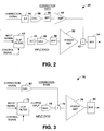
- FIG. 2 illustrates a schematic block diagram of an amplification system that combines a correction signal with an amplified peaked reduced input signal in accordance with an aspect of the present invention.
- FIG. 3 illustrates a schematic block diagram of an amplification system that combines a correction signal with a peaked reduced or clipped input signal prior to amplification in accordance with an aspect of the present invention.
- FIG. 4 illustrates a schematic block diagram of an amplification system that separates an input signal into a plurality of transmission sub-bands in accordance with an aspect of the present invention.
- FIG. 5 illustrates a schematic block diagram of an amplification system that combines a digital anti-peak signal with a digital input signal in accordance with an aspect of the present invention.
- FIG. 6 illustrates a schematic block diagram of an amplification system that combines an analog anti-peak signal with an analog input signal in accordance with an aspect of the present invention.
- FIG. 7 illustrates a schematic block diagram of an amplification system that employs a digital cross-cancellation technique in accordance with an aspect of the present invention.
- FIG. 8 illustrates a block diagram of a communication system in accordance with an aspect of the present invention.
- FIG. 9 illustrates a methodology for amplifying an input signal in accordance with an aspect of the present invention.
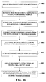
- FIG. 10 illustrates another methodology for amplifying an input signal in accordance with an aspect of the present invention.
- the present invention relates to an amplification system and method that reduces distortion and/or OOB emissions in amplifier systems such as those resulting from the clipping of peaks associated with an input signal.
- the system and method provide one or more corrections to the reduced peak signal associated with signal distortion and OOB emissions that result from the peak reduction. Therefore, smaller (less power capacity) and less costly power amplifiers can be employed to achieve similar performance.
- a second result is improved amplifier system efficiency as compared to amplifier systems with much larger less efficient power amplifiers.
- the present invention can be employed in wireless standards such as WCDMA, OFDM, multi-carrier versions of GSM and CDMA 2000 and other wireless standards and applications.
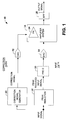
- FIG. 1 illustrates an amplification system 10 in accordance with an aspect of the present invention.
- the amplification system 10 includes a peak reduction component 12 that receives an input signal and generates a peak reduced input signal.
- the peak reduction component can clip peaks from the input signal by employing a clipping filter or the like to remove large peaks from the input signal.
- the peak reduction component 12 can be a peak reduction shaping algorithm.
- the peak reduction component can add signals (e.g., anti-peaking signals, anti-distortion signals) to the input signal to reduce peaks and distortions associated with the input signal.
- the peak reduction component can also perform pre-distortion on the peak reduced signal to mitigate errors to signal amplitude or phase and OOB emissions caused by the peak reduction.
- the above modifications can be performed individually, in combination or with other modification techniques to produce a peak reduced input signal that is optimal with respect to amplifier linearity, efficiency and power consumption.
- the choice of clipping option depends on the balance of allowable distortion in the wanted signal (e.g ., error vector magnitude, EVM) with constraints for OOB emissions.
- EVM error vector magnitude
- the OOB emissions that limit many clipping schemes, and to some extent, the distortion of the wanted signals, are cancelled by a dedicated subsystem before the signal is transmitted.
- the peak reduced input signal is transmitted to a digital-to-analog converter (DAC) 14.
- the DAC 14 converts the peak reduced input signal from the digital domain to the analog domain.
- the DAC can be a delta sigma modulated DAC (e.g ., 1-bit DAC) to perform a digital-to-analog conversion directly to radio transmission frequencies.
- a one-bit converter provides analog conversion with extremely high linearity (low distortion).
- the peak reduced input signal can be provided to a pre-distortion component 13 to remove at least a portion of the signal distortion and/or OOB emissions caused by the peak reduction. Employing pre-distortion reduces the remaining distortion so that components that are smaller, less costly and consume less power can be employed.
- the output of the DAC 14 is then provided to an amplifier system 16.
- the amplifier system 16 includes a power amplifier 24 for amplification of the peak reduced input signal.
- the power amplifier 24 can be a linear amplifier (e.g ., Class-A, Class-AB, Class-B) or, for some classes of input signal, it can be a non-linear type amplifier (e.g ., Class-C, Class-D, Class-E, Class-F) based on desired performance, acceptable efficiency and acceptable OOB emissions.
- the limit for WCDMA and many other wireless systems is the strict emissions mask in adjacent and nearby spectral channels which limits the amount of OOB that can be transmitted.
- the present invention illustrated in FIG. 1 is estimated to be able to correct 20-40 dB of OOB emissions.
- the OOB induced by clipping the wanted signal should be corrected by an amount to assure the OOB meets the emission mask of the relevant standard.
- the present invention allows for employment of a power amplifier that is smaller (less power).
- Efficiency of linear amplifiers (class A, A/B, B) which are prevalent in wireless systems is normally proportional to the PAR (class A degrades in efficiency about dB for dB of PAR, class B one-half dB per dB, and class A/B in-between), and thus the overall efficiency can be significantly improved with peak reduction.
- a class A/B amplifier transmitting a 10-dB PAR signal has total efficiency below 10% because most of the signals are extremely backed-off.
- the same transmitter can be made with double the efficiency at about 5 dB PAR employing the present invention.
- the low frequency of occurrence of the peaks enables the present invention to aggressively clip peaks without significant degradation of EVM.
- the increase in efficiency is critical in sizing the power handling, backup battery, and cooling equipment at a base station. The cost savings for these related systems can be comparable to the price of the transmitter.
- a correction signal generator 20 provides a correction signal to correct for signal distortion and OOB emissions caused by the peak reduction of the input signal.
- the signal distortion and OOB emissions can be mathematically computed based on the peak reduction that is performed. Therefore, a desired correction signal can be computed in real-time or off-line and programmed into the correction signal generator 20 ( e.g ., via a look-up table, a mathematical algorithm).
- the correction signal is transmitted to a second DAC 22.
- the second DAC 22 can also be a delta sigma modulated DAC to perform a digital-to-analog conversion directly to radio transmission frequencies of the correction signal.
- the analog correction signal is then provided to the amplifier system 16.
- the analog correction signal can be combined with the peak reduced input signal to mitigate signal distortion and OOB emissions prior to amplification by the power amplifier.
- the analog correction signal can be amplified and combined with the peak reduced input signal after amplification to mitigate signal distortion and OOB emissions in addition to distortions associated with amplification by the power amplifier.
- the output of the amplifier system 16 is then provided to an optional band pass filter 18, which filters out any remaining unwanted signals outside the desired transmission band to provide a final output signal substantially free of signal distortion and OOB emissions.
- the delta sigma DACs can be employed to upconvert the input signal directly to radio transmission frequencies, such that further frequency conversion of the signals via conventional analog mixers is not required.
- the radio transmission frequencies can be in radio frequency (RF) ranges (e.g. , megahertz range) or in microwave frequency ranges ( e.g ., gigahertz range).
- the correction signal can also be used purely for linearization in the absence of clipping or peak reduction. This may be desirable as DAC limitations in dynamic range over wide bandwidths can limit digital linearization techniques.
- the present invention separates the paths of wanted signal and correction signal allowing bandwidth and dynamic range requirements to be allocated over two or more DACs.
- a digital component such as a digital signal processor, provides the input signal, a control signal for controlling the clipping associated with the clipping filter and a correction signal to correct or mitigate OOB emissions caused by the clipping.
- the clipping filter 42 provides a clipped input signal to a delta sigma modulator 44 along an input path.
- the delta-sigma modulator 44 is coupled to a DAC 46 that is coupled to a band pass filter 48.
- the delta-sigma modulator 44, the DAC 46 and the band pass filter 48 cooperate to perform a digital-to-analog conversion directly to radio transmission frequencies.
- the DAC 46 can be a multi-bit converter or a one-bit converter that provides analog conversion with extremely high linearity (low distortion).
- the output of the band pass filter 48 is then provided to the input terminal of the power amplifier 50 for amplification.
- the power amplifier 50 can be a linear amplifier (e.g ., Class-A, Class-AB, Class-B) or, for some classes of input signal, it can be a non-linear type amplifier (e.g ., Class-C, Class-D, Class-E, Class-F) based on desired performance, acceptable efficiency and acceptable OOB emissions. Additional frequency conversion components can be employed as needed.
- the digital component (not shown) provides the correction signal along a correction path to a delta sigma modulator 56.
- the delta-sigma modulator 56 is coupled to a DAC 58, which is coupled to a band pass filter 60.
- the correction signal can be of substantially lower power compared to the wanted signal ( e.g ., typically 10-30 dB below the wanted signal level, prior to amplification by the power amplifier).
- the lower power level of the correction signal allows DAC 58 to be a lower dynamic range DAC than DAC 46. It can also have a wider bandwidth than DAC 46.
- the delta-sigma modulator 56, the DAC 58 and the band pass filter 60 cooperate to perform a digital-to-analog conversion directly to radio transmission frequencies.
- a class A, A/B amplifier that is well backed-off can be employed.
- the linearization of the cancellation amplifier 62 could be a pre-distortion system (analog or digital; the latter requiring digitizing and re-converting the signal), a feedforward loop or some other linearization technique.
- the size of the cancellation amplifier 62 is dependent on the required correction level (i.e., OOB emissions, signal distortions). Therefore, pre-distortion can be employed with the amplification system 40 to reduce the size of the correction amplifier 62.
- the correction amplifier 62 provides an amplified analog correction signal that can be combined with an analog output signal of the power amplifier 50 to mitigate OOB emissions and signal distortion of the analog output signal as a result of the clipping by the clipping filter 42.
- the analog correction signal of the cancellation amplifier 62 and the analog output signal of the power amplifier 50 are combined at a summer or coupler 52. It may be necessary to include either digital or analog delay components to synchronize the correction signal and output signal based on a particular implementation.
- the output of the summer 52 is then provided to an optional band pass filter 54, which filters out any remaining unwanted signals outside the desired transmission band.
- FIG. 3 illustrates an amplification system that combines a correction signal with a peaked reduced or clipped input signal prior to amplification in accordance with an aspect of the present invention.
- the amplification system 70 includes a clip filter 72 that performs a clipping process on an input signal.
- the clip filter 72 can be similar to the clip filter described in FIG. 2.
- the clipping process reduces the peaks of the input signal to reduce the PAR of the input signal provided to a power amplifier 78. This allows the power amplifier 78 to output a large average power associated with amplification of the clipped input signal.
- the clipping process can be performed via soft clipping, hard clipping, and/or a fixed or shape limiting algorithm to reduced the peaks and PAR associated with the input signal.
- the clipping process can result in unwanted OOB emissions, spectral distortions, spectral splatter and spectrum spreading.
- a digital component such as a digital signal processor, provides the input signal, a control signal for controlling the clipping associated with the clipping filter and a correction signal to correct or mitigate OOB emissions caused by the clipping.
- the clipping filter 72 provides the clipped input signal to a DAC 74 (e.g ., delta sigma modulated DAC) along an input path.
- the DAC 74 performs a digital-to-analog conversion of the clipped input signal, which can be converted directly to radio transmission frequencies, to produce an analog clipped input signal.
- the DAC 74 can be a multi-bit converter or a one-bit converter.
- the output of the DAC 74 is then provided to a summer or coupler 76.
- the digital component (not shown) provides the correction signal to a DAC 82 along a correction path, which converts the correction signal from the digital domain to the analog domain to produce an analog correction signal.
- the DAC 82 can be a multi-bit converter or a one-bit converter.
- the output of the DAC 82 is also provided to the summer or coupler 76, which combines the analog clipped input signal with the analog correction signal.
- the correction signal can be of substantially lower power compared to the wanted signal (e.g ., typically 10-30 dB below the wanted signal level (prior to amplification by the power amplifier)).
- the DAC 82 can be wider band and lower dynamic range than DAC 74.
- the analog correction signal mitigates OOB emissions and signal distortion without the need for employing a cancellation amplifier.
- the output of the summer 76 is provided to the input of the power amplifier 78 for amplification.
- the output of the amplifier 78 is then provided to an optional band pass filter 80, which filters out any remaining unwanted signals outside the desired
- At least one of the wanted signal, adjacent channels, and nearby spectral bands are decomposed into small frequency slices or sub-bands, each of which is modified in amplitude and phase and given an offset.
- these modified signals are digitized and amplified they cancel the OOB emissions resulting from the clipping.
- These modified slices are either aggregated before of after the digital-to-analog converter (DAC) operation, depending on the available DAC bandwidth, and amplified to final power levels. This technique can be applied to linearize the entire transmitter chain over wide bandwidths if distortions are predictable.
- DAC digital-to-analog converter
- This aspect of the present invention allows the correction terms to tailored to that portion of the spectrum and avoids the problem of digital pre-distortion where a single DAC supplies the bandwidth for the correction terms and dynamic range for the wanted signal and emission mask.
- An optional feedback loop digitizes and channelizes a sample of the output to enable adaptive improvement of the gain and phase modifications.
- an offset signal is added to each sub-band.
- the signal modifications are computed to cancel the OOB emissions and signal distortion that will be present after final amplification.
- This amplification system will provide optimized linearization and/or OOB emission reduction over each portion of the spectrum. The optimized linearization will occur if the clip filter 102 is removed.
- a summer 108 recombines the sub-bands into an aggregated or recombined input signal.
- the sub-bands can be combined later in the signal chain (e.g., after digital-to-analog conversion). Optimizing later in the signal chain requires additional DACs but allows each DAC to be optimized for bandwidth, dynamic range, and other performance parameters.
- the aggregated input signal is provided to a DAC 110 that converts the aggregated input signal from a digital signal to an analog aggregated input signal.
- the analog aggregated input signal is then provided to an optional surface acoustic wave (SAW) filter 112.
- SAW surface acoustic wave
- An optional ADC and digital channelizer can be provided to digitize a sample of the output and compare the sample of the output to the wanted signals to adaptively improve the gain, phase, and offset terms for each sub-band. Corrections signals can be provided to the signal prior to amplification and/or after amplification to facilitate cancellation of signal distortion and OOB emissions.
- the channelizer 104, the modification components 106 and the aggregation component 108 can be employed as a pre-distortion component for a variety of different amplification systems. Additionally, the channelizer 104, the modification components 106 and the aggregation component 108 can be employed as a pre-distortion component in an amplification system such as that illustrated in FIG. 1. Furthermore, the modification component 106 can provide the desired correction signals to the individual sub-bands in the form of or in addition to the gain, phase and offset adjustments.
- an additional signal that is designed to cancel the peaks of the wanted signals is added to the wanted signals.
- This signal can be filtered or cancelled prior to transmission so as not to cause errors to the intended receiver or other receivers in the area.
- the added signal is in the transmission band of the wanted signal but is orthogonal.
- the additional signal(s) may be added prior to and/or after digital-to-analog conversion occurs.
- FIG. 5 illustrates an amplification system 120 that combines a digital anti-peak signal with a digital input signal in accordance with an aspect of the present invention.
- the amplification system 120 includes an anti-peak signal component 122 that combines an anti-peak signal with an input signal to reduce peaks associated with an input signal, and to mitigate signal distortion and OOB emissions associated with either the reduction of the peaks or non-linearities in the signal chain.
- the combining of the input signal with the anti-peak signal reduces the peaks of the input signal and the PAR of the input signal provided to a power amplifier 130.
- the peak reduced input signal is transmitted to a delta sigma modulator 124 along an input path.
- the delta-sigma modulator 124 is coupled to a DAC 126, which is coupled to a band pass filter 128.
- the delta-sigma modulator 124, the DAC 126 and the band pass filter 128 cooperate to perform a digital-to-analog conversion directly to radio transmission frequencies.
- the DAC 126 can be a multi-bit converter or a one-bit converter that provides analog conversion with extremely high linearity (low distortion).
- the output of the band pass filter 128 is then provided to the input terminal of the power amplifier 130 for amplification to provide an amplified peak reduced output signal.
- the power amplifier 130 can be a linear amplifier (e.g., Class-A, Class-AB, Class-B) or, for some classes of input signal, it can be a non-linear type amplifier (e.g., Class-C, Class-D, Class-E, Class-F) based on desired performance, acceptable efficiency and acceptable OOB emissions.
- a linear amplifier e.g., Class-A, Class-AB, Class-B
- a non-linear type amplifier e.g., Class-C, Class-D, Class-E, Class-F
- a peak signal is provided to a delta sigma modulator 136 along a correction path.
- the peak signal is a substantial inversion of the anti-peak signal and removes the anti-peak signal from the final amplified output.
- the anti-peak signal can be removed via filtering, for example, by employing an orthogonal signal or output of band signal with the peak reduced input signal, and the signal losses are acceptable, addition of the peak signal may not be desired.
- the peak signal may also contain terms to reduce OOB emissions and/or reduce wanted signal distortion.
- the delta-sigma modulator 136 is coupled to a DAC 138, which is coupled to a band pass filter 140.
- the delta-sigma modulator 136, the DAC 138 and the band pass filter 140 cooperate to perform a digital-to-analog conversion directly to radio transmission frequencies.
- the DAC 138 can be a multi-bit converter or a one-bit converter.
- the output of the band pass filter 140 is then provided to the input terminal of a peak amplifier 142 for amplification.
- the peak amplifier 142 provides the amplified peak signal to a summer or coupler 132 to be aggregated with the output signal from the power amplifier 130 to remove the anti-peak signal from the final output.
- the output of the summer 132 is then provided to an optional band pass filter 134, which filters out any remaining unwanted signals outside the desired transmission band. It may be necessary to utilize digital or analog delay elements to synchronize the peak signal and output signal based on a particular implementation.
- FIG. 6 illustrates an amplification system that combines an anti-peak signal with an input signal prior to amplification in accordance with an aspect of the present invention.
- This variant of the present invention can be used to introduce an out-of-band anti-peaking signal that would otherwise be filtered prior to final amplification.
- the anti-peaking signal is designed not to result in appreciable OOB emissions from its interaction with the wanted signal.
- the amplification system 160 includes an anti-peak signal component 166 that generates an anti-peak signal based on an input signal.
- the input signal is provided to a first DAC 162, which converts the input signal from the digital domain to the analog domain to provide an analog input signal.
- the anti-peak signal is provided to a second DAC 168, which converts the anti-peak signal from the digital domain to the analog domain to provide an analog anti-peak signal.
- the analog anti-peak signal and the analog input signal are then combined at an analog summer or coupler 164.
- the combining of the anti-peak signal with the input signal reduces the PAR of the input signal provided to the power amplifier 170. This allows the power amplifier 170 to output a large average power associated with amplification of the peak reduced input signal.
- a peak signal is provided to a third DAC 176.
- the peak signal is a substantial inversion of the anti-peak signal and removes the anti-peak signal before final transmission.
- the third DAC 176 performs a digital-to-analog conversion directly to radio transmission frequencies.
- the third DAC 176 can be a multi-bit converter or a one-bit converter.
- the output of the third DAC 176 is then provided to the input terminal of a peak amplifier 178 for amplification.
- the peak amplifier 178 provides an amplified peak signal to a summer or coupler 172 to be aggregated with an analog output signal from the power amplifier 170.
- the amplified peak signal removes the anti-peak signal from the final output of the amplification system 160.
- the combined output of the summer 172 is then provided to an optional band pass filter 174, which filters out any remaining unwanted signals outside the desired transmission band.
- the peak reduced input signal is transmitted to a delta-sigma modulator 206 along an input path.
- the delta sigma modulator 206 is coupled to a DAC 208 (e.g ., 1-bit DAC, multi-bit DAC), which is coupled to a band pass filter 210.
- the delta-sigma modulator 206, the DAC 208 and the band pass filter 210 cooperate to perform a digital-to-analog conversion directly to radio transmission frequencies.
- the output of the band pass filter 210 is then provided to an optional driver amp 212, which provides additional gain to the analog input signal.
- the output of the driver 212 is then provided to the input terminal of the power amplifier 214 for amplification.
- the digital component 202 provides a reference signal along a correction path to a digital phase inverter 224.
- the reference signal is a reference version (REF) of the input signal corresponding to the desired amplified output signal prior to any modifications.
- the digital inverter 224 can be eliminated and the inverted version of the clean reference signal can be provided by the digital component 202.
- the inverted reference signal is transmitted to a delta-sigma modulator 226.
- the delta sigma modulator 226 is coupled to a DAC 228 (e.g ., 1-bit DAC, multi-bit DAC) and a band pass filter 230.
- the delta-sigma modulator 226, the DAC 228 and the band pass filter 230 cooperate to perform a digital-to-analog conversion directly to radio transmission frequencies of the inverted version of the clean reference signal (REF).
- the digital cross-cancellation technique in accordance with an aspect of the present invention can supply correction for amplifier and other non-linearities and it can correct spectral splatter that occurs from intentional clipping of the wanted signals performed to allow for amplifier size reduction. Additionally, since a digital reference signal is employed to determine the desired correction at the output, any modification of the signal can be corrected at the final output stage without the need for additional correction information during the amplification process.
- the various aspects of the invention illustrated in FIGS. 1-7 can be employed alone or in a variety of different combinations.
- the amplification system of the present invention can be employed in a number of applications and/or standards.
- the amplification system can be employed in wireless transmitter applications for base stations (e.g ., satellites, cellular), handsets, and other mobile communication devices.
- the present invention enables many transmitter architectures to operate with higher efficiency and substantially smaller part size and cost.
- a conventional four-carrier WCDMA system can save 50% or more on the most costly part of the transmitter, the final amplifier device. It can also improve its operating efficiency from less than10% to greater than 20% or more, enabling a significant cost savings in base station capital equipment.
- FIGS. 9-10 methodologies in accordance with various aspects of the present invention will be better appreciated with reference to FIGS. 9-10. While, for purposes of simplicity of explanation, the methodologies of FIGS. 9-10 are shown and described as executing serially, it is to be understood and appreciated that the present invention is not limited by the illustrated order, as some aspects could, in accordance with the present invention, occur in different orders and/or concurrently with other aspects from that shown and described herein. Moreover, not all illustrated features may be required to implement a methodology in accordance with an aspect the present invention.
- FIG. 9 illustrates a methodology for amplifying an input signal in accordance with an aspect of the present invention.
- the methodology begins at 300 where peaks associated with an input signal are reduced.
- the peaks associated with the input signal can be reduced by clipping the input signal via soft clipping and/or hard clipping employing a clipping filter or the like.
- the peaks associated with the input signal can also be reduced by employing a fixed or shaped peak limiting algorithm.
- the peaks associated with the input signal can be reduced by adding an ant-peaking signal to the input signal.
- One or more of the above peak reducing techniques can be employed alone or in combination to reduced peaks associated with the input signal.
- the input signal can be an input signal that conforms to a variety of different wireless formats (e.g., WCDMA, OFDM, multi-carrier versions of GSM, CDMA 2000).
- the methodology then proceeds to 310.
- a correction signal is generated to mitigate one or more of OOB emissions and signal distortion associated with the peak reduction of the input signal.
- pre-distortion is performed on the peak reduced input signal to mitigate at least a portion of one or more of the OOB emissions and signal distortion associated with the peak reduction.
- the peak reduced input signal and the correction signal are converted from the digital domain to the analog domain, for example, via separate associated DACs. Separating the paths of the wanted signal and correction signal allows bandwidth and dynamic range requirements to be allocated over two or more DACs. The methodology then proceeds to 340.
- the modified sub-band signals are converted from the digital domain to the analog domain.
- the modified analog sub-band signals are aggregated or recombined to provide a recombined analog input signal.
- the aggregation may occur prior to conversion to the analog domain.
- the aggregated signal will have mitigated OOB emissions due to clipping and may contain additional linearization terms.
- the aggregated analog input signal is optionally filtered by an acoustic wave (SAW) filter or the like.
- the aggregated analog input signal is then amplified to provide a final amplified output signal for transmission over a wireless link.
- One or more additional signals can be added to the aggregated signal prior to amplification or after amplification to mitigate any remaining signal distortion and OOB emissions.
- the amplified signal is passed through an optional bandpass filter to remove signals outside of the transmission band at 470.
Landscapes
- Physics & Mathematics (AREA)
- Nonlinear Science (AREA)
- Engineering & Computer Science (AREA)
- Power Engineering (AREA)
- Amplifiers (AREA)
- Transmitters (AREA)
Applications Claiming Priority (2)
| Application Number | Priority Date | Filing Date | Title |
|---|---|---|---|
| US10/625,367 US7042287B2 (en) | 2003-07-23 | 2003-07-23 | System and method for reducing dynamic range and improving linearity in an amplication system |
| US625367 | 2003-07-23 |
Publications (2)
| Publication Number | Publication Date |
|---|---|
| EP1501187A1 true EP1501187A1 (de) | 2005-01-26 |
| EP1501187B1 EP1501187B1 (de) | 2008-03-26 |
Family
ID=33490882
Family Applications (1)
| Application Number | Title | Priority Date | Filing Date |
|---|---|---|---|
| EP04017347A Expired - Lifetime EP1501187B1 (de) | 2003-07-23 | 2004-07-22 | System und Verfahren zur Reduktion der Dynamik und Erhöhung der Linearität in einem Verstärkersystem |
Country Status (4)
| Country | Link |
|---|---|
| US (2) | US7042287B2 (de) |
| EP (1) | EP1501187B1 (de) |
| JP (1) | JP2005045817A (de) |
| DE (1) | DE602004012671T2 (de) |
Cited By (1)
| Publication number | Priority date | Publication date | Assignee | Title |
|---|---|---|---|---|
| EP2330734A1 (de) * | 2009-11-25 | 2011-06-08 | Alcatel Lucent | Leistungsverstärkervorrichtung mit digitaler Delta-Sigma-Modulation und ein Impuls mit Modulator sowie Verfahren dafür |
Families Citing this family (64)
| Publication number | Priority date | Publication date | Assignee | Title |
|---|---|---|---|---|
| US8380143B2 (en) | 2002-05-01 | 2013-02-19 | Dali Systems Co. Ltd | Power amplifier time-delay invariant predistortion methods and apparatus |
| US6985704B2 (en) | 2002-05-01 | 2006-01-10 | Dali Yang | System and method for digital memorized predistortion for wireless communication |
| US8811917B2 (en) | 2002-05-01 | 2014-08-19 | Dali Systems Co. Ltd. | Digital hybrid mode power amplifier system |
| US8472897B1 (en) | 2006-12-22 | 2013-06-25 | Dali Systems Co. Ltd. | Power amplifier predistortion methods and apparatus |
| GB2398648B (en) * | 2003-02-19 | 2005-11-09 | Nujira Ltd | Power supply stage for an amplifier |
| JP2005106684A (ja) * | 2003-09-30 | 2005-04-21 | Konica Minolta Medical & Graphic Inc | 放射線画像変換パネル及びその製造方法 |
| US7542517B2 (en) * | 2004-02-02 | 2009-06-02 | Ibiquity Digital Corporation | Peak-to-average power reduction for FM OFDM transmission |
| US7305041B2 (en) * | 2004-02-20 | 2007-12-04 | Kiomars Anvari | Peak suppression of multi-carrier signal with different modulation |
| JP4359191B2 (ja) * | 2004-06-01 | 2009-11-04 | 株式会社日立国際電気 | 信号生成装置 |
| BRPI0515126A (pt) * | 2004-08-30 | 2008-07-08 | Matsushita Electric Industrial Co Ltd | aparelho de supressão de potência de crusta e método de supressão de potência de crista |
| US7327803B2 (en) | 2004-10-22 | 2008-02-05 | Parkervision, Inc. | Systems and methods for vector power amplification |
| US7355470B2 (en) | 2006-04-24 | 2008-04-08 | Parkervision, Inc. | Systems and methods of RF power transmission, modulation, and amplification, including embodiments for amplifier class transitioning |
| US7764729B1 (en) * | 2005-03-25 | 2010-07-27 | Lockheed Martin Corporation | Channelized amplifier system and method |
| US7542736B2 (en) * | 2005-07-26 | 2009-06-02 | M/A-Com, Inc. | Techniques to decrease signal amplitude peak-to-average ratio in a wireless communications system |
| US20130078934A1 (en) | 2011-04-08 | 2013-03-28 | Gregory Rawlins | Systems and Methods of RF Power Transmission, Modulation, and Amplification |
| US7911272B2 (en) | 2007-06-19 | 2011-03-22 | Parkervision, Inc. | Systems and methods of RF power transmission, modulation, and amplification, including blended control embodiments |
| US8013675B2 (en) | 2007-06-19 | 2011-09-06 | Parkervision, Inc. | Combiner-less multiple input single output (MISO) amplification with blended control |
| US7944991B2 (en) * | 2005-10-27 | 2011-05-17 | Georgia Tech Research Corporation | Constrained clipping for peak-to-average power ratio (crest factor) reduction in multicarrier transmission systems |
| US7362170B2 (en) * | 2005-12-01 | 2008-04-22 | Andrew Corporation | High gain, high efficiency power amplifier |
| US7831221B2 (en) * | 2005-12-13 | 2010-11-09 | Andrew Llc | Predistortion system and amplifier for addressing group delay modulation |
| JP4750592B2 (ja) * | 2006-03-17 | 2011-08-17 | 富士通株式会社 | ピーク抑圧方法、ピーク抑圧装置、無線送信装置 |
| US7937106B2 (en) | 2006-04-24 | 2011-05-03 | ParkerVision, Inc, | Systems and methods of RF power transmission, modulation, and amplification, including architectural embodiments of same |
| US8031804B2 (en) | 2006-04-24 | 2011-10-04 | Parkervision, Inc. | Systems and methods of RF tower transmission, modulation, and amplification, including embodiments for compensating for waveform distortion |
| CN101479956B (zh) * | 2006-04-28 | 2013-07-31 | 大力系统有限公司 | 用于无线通信的高效率线性化功率放大器 |
| US7983327B2 (en) * | 2006-08-28 | 2011-07-19 | Samsung Electronics Co., Ltd. | Method and system for providing digital adaptive predistortion in a subscriber station |
| WO2008048771A2 (en) * | 2006-10-18 | 2008-04-24 | The Regents Of The University Of California | Pulsed load modulation amplifier and method |
| US9026067B2 (en) * | 2007-04-23 | 2015-05-05 | Dali Systems Co. Ltd. | Remotely reconfigurable power amplifier system and method |
| CN104202279A (zh) | 2006-12-26 | 2014-12-10 | 大力系统有限公司 | 用于多信道宽带通信系统中的基带预失真线性化的方法和系统 |
| US7620129B2 (en) | 2007-01-16 | 2009-11-17 | Parkervision, Inc. | RF power transmission, modulation, and amplification, including embodiments for generating vector modulation control signals |
| US8825065B2 (en) * | 2007-01-19 | 2014-09-02 | Wi-Lan, Inc. | Transmit power dependent reduced emissions from a wireless transceiver |
| US8290447B2 (en) * | 2007-01-19 | 2012-10-16 | Wi-Lan Inc. | Wireless transceiver with reduced transmit emissions |
| JP2008197284A (ja) * | 2007-02-09 | 2008-08-28 | Sharp Corp | フィルタ係数算出装置、フィルタ係数算出方法、制御プログラム、コンピュータ読み取り可能な記録媒体、および、音声信号処理装置 |
| US7787564B1 (en) * | 2007-03-13 | 2010-08-31 | Kiomars Anvari | Combined peak reduction equalizer and phase/amplitude pre-distortion |
| KR101484796B1 (ko) * | 2007-04-23 | 2015-01-20 | 달리 시스템즈 씨오. 엘티디. | N-웨이 도허티 분산형 전력 증폭기 |
| US8274332B2 (en) | 2007-04-23 | 2012-09-25 | Dali Systems Co. Ltd. | N-way Doherty distributed power amplifier with power tracking |
| WO2008144017A1 (en) | 2007-05-18 | 2008-11-27 | Parkervision, Inc. | Systems and methods of rf power transmission, modulation, and amplification |
| WO2009005768A1 (en) | 2007-06-28 | 2009-01-08 | Parkervision, Inc. | Systems and methods of rf power transmission, modulation, and amplification |
| US8224266B2 (en) * | 2007-08-30 | 2012-07-17 | Dali Systems Co., Ltd. | Power amplifier predistortion methods and apparatus using envelope and phase detector |
| WO2009060652A1 (ja) | 2007-11-05 | 2009-05-14 | Nec Corporation | 電力増幅器およびこれを備える電波送信機 |
| KR101669173B1 (ko) * | 2007-12-07 | 2016-10-25 | 달리 시스템즈 씨오. 엘티디. | 베이스밴드-도출형 광대역 rf 디지털 전치 왜곡 시스템 |
| WO2009145887A1 (en) | 2008-05-27 | 2009-12-03 | Parkervision, Inc. | Systems and methods of rf power transmission, modulation, and amplification |
| US8331879B2 (en) * | 2008-10-15 | 2012-12-11 | Research In Motion Limited | Multi-dimensional Volterra series transmitter linearization |
| US8396432B2 (en) | 2009-07-01 | 2013-03-12 | Panasonic Corporation | Transmitter circuit and communication apparatus |
| KR20110026065A (ko) * | 2009-09-07 | 2011-03-15 | 삼성전자주식회사 | 무선통신 시스템에서 전력 제어를 지원하는 포락선 추적 전력 증폭기를 위한 장치 및 방법 |
| JP5249254B2 (ja) * | 2010-01-21 | 2013-07-31 | アズビル株式会社 | 変調器およびδς型d/a変換器 |
| CN105141513B (zh) | 2010-09-14 | 2018-12-14 | 大力系统有限公司 | 操作分布式天线系统的方法和在该系统中进行通信的方法 |
| US8204456B2 (en) * | 2010-09-15 | 2012-06-19 | Fujitsu Semiconductor Limited | Systems and methods for spurious emission cancellation |
| JP2012142840A (ja) * | 2011-01-05 | 2012-07-26 | Mitsubishi Electric Corp | 歪み補償回路装置 |
| EP2715867A4 (de) | 2011-06-02 | 2014-12-17 | Parkervision Inc | Antennensteuerung |
| US8798194B2 (en) | 2011-12-15 | 2014-08-05 | Intel Mobile Communications GmbH | Adaptive compensation of nonlinear frequency distortion in polar transmitters based on a least squares estimation |
| US8638878B2 (en) | 2011-12-15 | 2014-01-28 | Intel Mobile Communications GmbH | Method and faculty to measure and compensate DCO frequency distortions using a DPLL |
| US8867660B2 (en) * | 2011-12-15 | 2014-10-21 | Intel Mobile Communications GmbH | Method and system to measure and compensate undue DCO frequency peaks at GFSK ramp down |
| US8692700B2 (en) * | 2012-05-02 | 2014-04-08 | Honeywell International Inc. | Sigma-delta digital-to-analog converter |
| JP5958309B2 (ja) * | 2012-12-03 | 2016-07-27 | 富士通株式会社 | 無線通信装置、ドハティ増幅器及び無線通信装置の制御方法 |
| US9042469B2 (en) * | 2013-07-08 | 2015-05-26 | National Chiao Tung University | Receiver and receiving method for a combinerless LINC OFDM system |
| WO2015042142A1 (en) | 2013-09-17 | 2015-03-26 | Parkervision, Inc. | Method, apparatus and system for rendering an information bearing function of time |
| US9172570B1 (en) | 2014-06-13 | 2015-10-27 | Intel IP Corporation | Compensation of oscillator frequency pulling |
| US9590664B2 (en) * | 2015-02-16 | 2017-03-07 | Telefonaktiebolaget Lm Ericsson (Publ) | Method to improve active antenna system performance in the presence of mutual coupling |
| EP3311497B1 (de) * | 2015-06-16 | 2021-08-04 | Commscope Technologies LLC | Funkfrequenzsender |
| KR20170118913A (ko) * | 2016-01-19 | 2017-10-25 | 후아웨이 테크놀러지 컴퍼니 리미티드 | 오차 보상 직접 디지털 변조 장치 |
| US11108403B2 (en) * | 2017-04-13 | 2021-08-31 | Rohde & Schwarz Gmbh & Co. Kg | Device and method for efficient digital-analog conversion |
| CN109586677B (zh) * | 2017-09-29 | 2020-12-25 | 华为技术有限公司 | 信号处理装置、多输入功率放大系统及相关方法 |
| US12267094B2 (en) * | 2019-09-13 | 2025-04-01 | The Regents Of The University Of California | Spectrum-compressing receiver and reception method for non-contiguous carrier aggregation |
| DE102023200140B3 (de) | 2023-01-10 | 2024-06-13 | Bruker Biospin Gmbh | Schaltungsanordnung zum Korrigieren eines Eingangssignals, Verwendung der Schaltungsanordnung zur Erfassung eines physiologischen Signals in einem Magnetresonanz-(MR)-System |
Citations (3)
| Publication number | Priority date | Publication date | Assignee | Title |
|---|---|---|---|---|
| US4596043A (en) * | 1982-03-29 | 1986-06-17 | Motorola, Inc. | High efficiency radio frequency signal amplifier for amplifying modulated radio frequency signals in a manner generating minimal splatter |
| EP1065856A2 (de) * | 1999-06-17 | 2001-01-03 | Itelco - S.p.A. | Basisbandvorverzerrungssystem für die linearisierung von Leistungsverstärker |
| US20030091123A1 (en) * | 2001-11-12 | 2003-05-15 | Evolium S.A.S. | Method of clipping signal comprising a plurality of carriers transmitted by the same non-linear amplifier |
Family Cites Families (16)
| Publication number | Priority date | Publication date | Assignee | Title |
|---|---|---|---|---|
| US91123A (en) * | 1869-06-08 | Improvement in homomotive | ||
| US101936A (en) * | 1870-04-12 | Improvement in churns | ||
| DE19635813A1 (de) | 1996-09-04 | 1998-03-05 | Johannes Prof Dr Ing Huber | Verfahren zur Reduktion des Spitzenwertfaktors bei digitalen Übertragungsverfahren |
| US5862452A (en) | 1997-10-20 | 1999-01-19 | Motorola, Inc. | Method, access point device and peripheral devices for low complexity dynamic persistence mode for random access in a wireless communication system |
| US5886573A (en) * | 1998-03-06 | 1999-03-23 | Fujant, Inc. | Amplification using amplitude reconstruction of amplitude and/or angle modulated carrier |
| US6356606B1 (en) | 1998-07-31 | 2002-03-12 | Lucent Technologies Inc. | Device and method for limiting peaks of a signal |
| US6097930A (en) * | 1998-08-21 | 2000-08-01 | Weblink Wireless, Inc. | System and method for modeling simulcast delay spread and optimizing launch delays |
| US6798843B1 (en) * | 1999-07-13 | 2004-09-28 | Pmc-Sierra, Inc. | Wideband digital predistortion linearizer for nonlinear amplifiers |
| US6395483B1 (en) * | 1999-09-02 | 2002-05-28 | 3M Innovative Properties Company | Arrays with mask layers |
| US6449302B2 (en) | 2000-04-19 | 2002-09-10 | Powerwave Technologies, Inc. | System and method for peak power reduction in spread spectrum communications systems |
| US6300826B1 (en) * | 2000-05-05 | 2001-10-09 | Ericsson Telefon Ab L M | Apparatus and method for efficiently amplifying wideband envelope signals |
| JP3877937B2 (ja) | 2000-05-18 | 2007-02-07 | 株式会社エヌ・ティ・ティ・ドコモ | フィードフォワード増幅器 |
| US6633200B2 (en) * | 2000-06-22 | 2003-10-14 | Celiant Corporation | Management of internal signal levels and control of the net gain for a LINC amplifier |
| US7061990B2 (en) | 2000-07-21 | 2006-06-13 | Pmc-Sierra Inc. | Systems and methods for the dynamic range compression of multi-bearer single-carrier and multi-carrier waveforms |
| US6794936B2 (en) * | 2001-07-03 | 2004-09-21 | Lucent Technologies Inc. | Equalizer system and method for predistortion |
| US6600369B2 (en) * | 2001-12-07 | 2003-07-29 | Motorola, Inc. | Wideband linear amplifier with predistortion error correction |
-
2003
- 2003-07-23 US US10/625,367 patent/US7042287B2/en not_active Expired - Lifetime
-
2004
- 2004-07-22 DE DE602004012671T patent/DE602004012671T2/de not_active Expired - Lifetime
- 2004-07-22 EP EP04017347A patent/EP1501187B1/de not_active Expired - Lifetime
- 2004-07-23 JP JP2004216350A patent/JP2005045817A/ja active Pending
-
2005
- 2005-01-20 US US11/038,959 patent/US7057455B2/en not_active Expired - Lifetime
Patent Citations (3)
| Publication number | Priority date | Publication date | Assignee | Title |
|---|---|---|---|---|
| US4596043A (en) * | 1982-03-29 | 1986-06-17 | Motorola, Inc. | High efficiency radio frequency signal amplifier for amplifying modulated radio frequency signals in a manner generating minimal splatter |
| EP1065856A2 (de) * | 1999-06-17 | 2001-01-03 | Itelco - S.p.A. | Basisbandvorverzerrungssystem für die linearisierung von Leistungsverstärker |
| US20030091123A1 (en) * | 2001-11-12 | 2003-05-15 | Evolium S.A.S. | Method of clipping signal comprising a plurality of carriers transmitted by the same non-linear amplifier |
Cited By (1)
| Publication number | Priority date | Publication date | Assignee | Title |
|---|---|---|---|---|
| EP2330734A1 (de) * | 2009-11-25 | 2011-06-08 | Alcatel Lucent | Leistungsverstärkervorrichtung mit digitaler Delta-Sigma-Modulation und ein Impuls mit Modulator sowie Verfahren dafür |
Also Published As
| Publication number | Publication date |
|---|---|
| US20050129140A1 (en) | 2005-06-16 |
| DE602004012671T2 (de) | 2009-05-07 |
| JP2005045817A (ja) | 2005-02-17 |
| US20050017800A1 (en) | 2005-01-27 |
| US7057455B2 (en) | 2006-06-06 |
| DE602004012671D1 (de) | 2008-05-08 |
| US7042287B2 (en) | 2006-05-09 |
| EP1501187B1 (de) | 2008-03-26 |
Similar Documents
| Publication | Publication Date | Title |
|---|---|---|
| EP1501187B1 (de) | System und Verfahren zur Reduktion der Dynamik und Erhöhung der Linearität in einem Verstärkersystem | |
| US7129778B2 (en) | Digital cross cancellation system | |
| US6987417B2 (en) | Polar and linear amplifier system | |
| US7043213B2 (en) | Multi-mode amplifier system | |
| EP1536556B1 (de) | Schaltverstärkerarchitektur | |
| US7034614B2 (en) | Modified polar amplifier architecture | |
| EP1685646B1 (de) | Verstärkersystem mit variabler versorgung | |
| EP1492228B1 (de) | Verstärkerarchitektur für mehreren Betriebsarten | |
| US6998914B2 (en) | Multiple polar amplifier architecture | |
| US7580476B2 (en) | Communication system and method for improving efficiency and linearity | |
| US8249530B2 (en) | Apparatus and method for power amplification in wireless communication system | |
| KR100810322B1 (ko) | 이동 통신용 고효율 전력 증폭 장치 및 방법 | |
| HK1195829A (en) | System and method for increasing bandwidth for digital predistortion in multi-channel wideband communication systems | |
| HK1195829B (en) | System and method for increasing bandwidth for digital predistortion in multi-channel wideband communication systems |
Legal Events
| Date | Code | Title | Description |
|---|---|---|---|
| PUAI | Public reference made under article 153(3) epc to a published international application that has entered the european phase |
Free format text: ORIGINAL CODE: 0009012 |
|
| AK | Designated contracting states |
Kind code of ref document: A1 Designated state(s): AT BE BG CH CY CZ DE DK EE ES FI FR GB GR HU IE IT LI LU MC NL PL PT RO SE SI SK TR |
|
| AX | Request for extension of the european patent |
Extension state: AL HR LT LV MK |
|
| 17P | Request for examination filed |
Effective date: 20041223 |
|
| AKX | Designation fees paid |
Designated state(s): DE FI FR GB NL |
|
| GRAP | Despatch of communication of intention to grant a patent |
Free format text: ORIGINAL CODE: EPIDOSNIGR1 |
|
| GRAS | Grant fee paid |
Free format text: ORIGINAL CODE: EPIDOSNIGR3 |
|
| GRAA | (expected) grant |
Free format text: ORIGINAL CODE: 0009210 |
|
| AK | Designated contracting states |
Kind code of ref document: B1 Designated state(s): DE FI FR GB NL |
|
| REG | Reference to a national code |
Ref country code: GB Ref legal event code: FG4D |
|
| REF | Corresponds to: |
Ref document number: 602004012671 Country of ref document: DE Date of ref document: 20080508 Kind code of ref document: P |
|
| PG25 | Lapsed in a contracting state [announced via postgrant information from national office to epo] |
Ref country code: FI Free format text: LAPSE BECAUSE OF FAILURE TO SUBMIT A TRANSLATION OF THE DESCRIPTION OR TO PAY THE FEE WITHIN THE PRESCRIBED TIME-LIMIT Effective date: 20080326 |
|
| NLV1 | Nl: lapsed or annulled due to failure to fulfill the requirements of art. 29p and 29m of the patents act | ||
| PG25 | Lapsed in a contracting state [announced via postgrant information from national office to epo] |
Ref country code: NL Free format text: LAPSE BECAUSE OF FAILURE TO SUBMIT A TRANSLATION OF THE DESCRIPTION OR TO PAY THE FEE WITHIN THE PRESCRIBED TIME-LIMIT Effective date: 20080326 |
|
| EN | Fr: translation not filed | ||
| PLBE | No opposition filed within time limit |
Free format text: ORIGINAL CODE: 0009261 |
|
| STAA | Information on the status of an ep patent application or granted ep patent |
Free format text: STATUS: NO OPPOSITION FILED WITHIN TIME LIMIT |
|
| 26N | No opposition filed |
Effective date: 20081230 |
|
| GBPC | Gb: european patent ceased through non-payment of renewal fee |
Effective date: 20080722 |
|
| PG25 | Lapsed in a contracting state [announced via postgrant information from national office to epo] |
Ref country code: FR Free format text: LAPSE BECAUSE OF FAILURE TO SUBMIT A TRANSLATION OF THE DESCRIPTION OR TO PAY THE FEE WITHIN THE PRESCRIBED TIME-LIMIT Effective date: 20090116 |
|
| PG25 | Lapsed in a contracting state [announced via postgrant information from national office to epo] |
Ref country code: GB Free format text: LAPSE BECAUSE OF NON-PAYMENT OF DUE FEES Effective date: 20080722 |
|
| REG | Reference to a national code |
Ref country code: DE Ref legal event code: R082 Ref document number: 602004012671 Country of ref document: DE Representative=s name: WUESTHOFF & WUESTHOFF PATENT- UND RECHTSANWAEL, DE |
|
| REG | Reference to a national code |
Ref country code: DE Ref legal event code: R081 Ref document number: 602004012671 Country of ref document: DE Owner name: NORTHROP GRUMMAN SYSTEMS CORPORATION, US Free format text: FORMER OWNER: NORTHROP GRUMMAN CORP., LOS ANGELES, US Effective date: 20120814 Ref country code: DE Ref legal event code: R082 Ref document number: 602004012671 Country of ref document: DE Representative=s name: WUESTHOFF & WUESTHOFF PATENT- UND RECHTSANWAEL, DE Effective date: 20120814 Ref country code: DE Ref legal event code: R081 Ref document number: 602004012671 Country of ref document: DE Owner name: NORTHROP GRUMMAN SYSTEMS CORPORATION, LOS ANGE, US Free format text: FORMER OWNER: NORTHROP GRUMMAN CORP., LOS ANGELES, CALIF., US Effective date: 20120814 Ref country code: DE Ref legal event code: R082 Ref document number: 602004012671 Country of ref document: DE Representative=s name: WUESTHOFF & WUESTHOFF, PATENTANWAELTE PARTG MB, DE Effective date: 20120814 |
|
| PGFP | Annual fee paid to national office [announced via postgrant information from national office to epo] |
Ref country code: DE Payment date: 20170724 Year of fee payment: 14 |
|
| REG | Reference to a national code |
Ref country code: DE Ref legal event code: R119 Ref document number: 602004012671 Country of ref document: DE |
|
| PG25 | Lapsed in a contracting state [announced via postgrant information from national office to epo] |
Ref country code: DE Free format text: LAPSE BECAUSE OF NON-PAYMENT OF DUE FEES Effective date: 20190201 |