EP1536556B1 - Schaltverstärkerarchitektur - Google Patents
Schaltverstärkerarchitektur Download PDFInfo
- Publication number
- EP1536556B1 EP1536556B1 EP04025039A EP04025039A EP1536556B1 EP 1536556 B1 EP1536556 B1 EP 1536556B1 EP 04025039 A EP04025039 A EP 04025039A EP 04025039 A EP04025039 A EP 04025039A EP 1536556 B1 EP1536556 B1 EP 1536556B1
- Authority
- EP
- European Patent Office
- Prior art keywords
- amplifier
- input signal
- level
- signal
- supply
- Prior art date
- Legal status (The legal status is an assumption and is not a legal conclusion. Google has not performed a legal analysis and makes no representation as to the accuracy of the status listed.)
- Expired - Lifetime
Links
- 230000004044 response Effects 0.000 claims description 7
- 230000003321 amplification Effects 0.000 description 41
- 238000003199 nucleic acid amplification method Methods 0.000 description 41
- 238000000034 method Methods 0.000 description 17
- 230000005540 biological transmission Effects 0.000 description 10
- 238000004891 communication Methods 0.000 description 8
- 238000010586 diagram Methods 0.000 description 5
- 239000000969 carrier Substances 0.000 description 3
- 238000006243 chemical reaction Methods 0.000 description 3
- 238000001816 cooling Methods 0.000 description 3
- 238000012937 correction Methods 0.000 description 3
- 238000004519 manufacturing process Methods 0.000 description 3
- 238000010295 mobile communication Methods 0.000 description 3
- 230000004048 modification Effects 0.000 description 3
- 238000012986 modification Methods 0.000 description 3
- 230000009467 reduction Effects 0.000 description 3
- 238000001228 spectrum Methods 0.000 description 3
- 230000001413 cellular effect Effects 0.000 description 2
- 239000002131 composite material Substances 0.000 description 2
- 238000005516 engineering process Methods 0.000 description 2
- 230000002401 inhibitory effect Effects 0.000 description 2
- 238000013316 zoning Methods 0.000 description 2
- JBRZTFJDHDCESZ-UHFFFAOYSA-N AsGa Chemical compound [As]#[Ga] JBRZTFJDHDCESZ-UHFFFAOYSA-N 0.000 description 1
- JMASRVWKEDWRBT-UHFFFAOYSA-N Gallium nitride Chemical compound [Ga]#N JMASRVWKEDWRBT-UHFFFAOYSA-N 0.000 description 1
- GPXJNWSHGFTCBW-UHFFFAOYSA-N Indium phosphide Chemical compound [In]#P GPXJNWSHGFTCBW-UHFFFAOYSA-N 0.000 description 1
- XUIMIQQOPSSXEZ-UHFFFAOYSA-N Silicon Chemical compound [Si] XUIMIQQOPSSXEZ-UHFFFAOYSA-N 0.000 description 1
- 230000004075 alteration Effects 0.000 description 1
- 230000003466 anti-cipated effect Effects 0.000 description 1
- 230000008901 benefit Effects 0.000 description 1
- 230000008859 change Effects 0.000 description 1
- 230000006835 compression Effects 0.000 description 1
- 238000007906 compression Methods 0.000 description 1
- 230000003111 delayed effect Effects 0.000 description 1
- 230000009977 dual effect Effects 0.000 description 1
- 230000006870 function Effects 0.000 description 1
- 230000007246 mechanism Effects 0.000 description 1
- 229910044991 metal oxide Inorganic materials 0.000 description 1
- 150000004706 metal oxides Chemical class 0.000 description 1
- 230000010363 phase shift Effects 0.000 description 1
- 230000008569 process Effects 0.000 description 1
- 238000012545 processing Methods 0.000 description 1
- 239000004065 semiconductor Substances 0.000 description 1
- 238000007493 shaping process Methods 0.000 description 1
- 229910052710 silicon Inorganic materials 0.000 description 1
- 239000010703 silicon Substances 0.000 description 1
- 230000003595 spectral effect Effects 0.000 description 1
- 230000007704 transition Effects 0.000 description 1
Images


Classifications
-
- H—ELECTRICITY
- H03—ELECTRONIC CIRCUITRY
- H03F—AMPLIFIERS
- H03F3/00—Amplifiers with only discharge tubes or only semiconductor devices as amplifying elements
- H03F3/20—Power amplifiers, e.g. Class B amplifiers, Class C amplifiers
- H03F3/21—Power amplifiers, e.g. Class B amplifiers, Class C amplifiers with semiconductor devices only
- H03F3/217—Class D power amplifiers; Switching amplifiers
-
- H—ELECTRICITY
- H03—ELECTRONIC CIRCUITRY
- H03F—AMPLIFIERS
- H03F1/00—Details of amplifiers with only discharge tubes, only semiconductor devices or only unspecified devices as amplifying elements
- H03F1/02—Modifications of amplifiers to raise the efficiency, e.g. gliding Class A stages, use of an auxiliary oscillation
- H03F1/0205—Modifications of amplifiers to raise the efficiency, e.g. gliding Class A stages, use of an auxiliary oscillation in transistor amplifiers
- H03F1/0211—Modifications of amplifiers to raise the efficiency, e.g. gliding Class A stages, use of an auxiliary oscillation in transistor amplifiers with control of the supply voltage or current
- H03F1/0216—Continuous control
- H03F1/0222—Continuous control by using a signal derived from the input signal
- H03F1/0227—Continuous control by using a signal derived from the input signal using supply converters
-
- H—ELECTRICITY
- H03—ELECTRONIC CIRCUITRY
- H03F—AMPLIFIERS
- H03F1/00—Details of amplifiers with only discharge tubes, only semiconductor devices or only unspecified devices as amplifying elements
- H03F1/02—Modifications of amplifiers to raise the efficiency, e.g. gliding Class A stages, use of an auxiliary oscillation
- H03F1/0205—Modifications of amplifiers to raise the efficiency, e.g. gliding Class A stages, use of an auxiliary oscillation in transistor amplifiers
- H03F1/0288—Modifications of amplifiers to raise the efficiency, e.g. gliding Class A stages, use of an auxiliary oscillation in transistor amplifiers using a main and one or several auxiliary peaking amplifiers whereby the load is connected to the main amplifier using an impedance inverter, e.g. Doherty amplifiers
-
- H—ELECTRICITY
- H03—ELECTRONIC CIRCUITRY
- H03F—AMPLIFIERS
- H03F2200/00—Indexing scheme relating to amplifiers
- H03F2200/331—Sigma delta modulation being used in an amplifying circuit
Definitions
- the present invention relates generally to electronic devices, and more particularly to a switching amplifier architecture.
- Modern transmitters for applications such as cellular, personal, and satellite communications employ digital modulation techniques such as quadrature phase-shift keying (QPSK) in combination with code division multiple access (CDMA) communication. Shaping of the data pulses mitigates out-of-band emissions from occurring into adjacent channels but produces time-varying envelopes.
- QPSK quadrature phase-shift keying
- CDMA code division multiple access
- Shaping of the data pulses mitigates out-of-band emissions from occurring into adjacent channels but produces time-varying envelopes.
- many transmitters (especially in base stations) are being configured to amplify multiple carriers.
- Multi-carrier signals have high a wide distribution of power levels resulting in a large peak-to-average ratio (PAR). Therefore, the operation of amplifiers (e.g.
- linear amplifiers in these types of signals is very inefficient, since the amplifiers must have their supply voltage sized to handle the large peak voltages even though the signals are much smaller a substantial portion of the time. Additionally, the size and cost of the power amplifier is generally proportional to the required peak output power of the amplifier.
- WCDMA Wideband Code Division Multiple Access
- OFDM Orthogonal Frequency Division Multiplexing
- GSM Global Standard for Mobile Communication
- CDMA 2000 Code Division Multiple Access 2000
- Switching amplifiers e.g. , Class C, D, or S type amplifiers
- Switching amplifiers switch between and "ON” and an "OFF" state nominally only using quiescent power during the transitions between "ON” and “OFF”.
- Their efficiency is very high when amplifying signals with a binary format, in response to a pulse width modulated signal that drives the transistors of the switching amplifier, or to carefully limited/clamped signals.
- Switching amplifiers are more efficient than linear classes of operation such as Class-A, Class-AB or Class-B type which conduct during at least half of the RF cycle and are significantly backed off from compression.
- Switching amplifiers provide very high (>70% and as high as 95%) efficiency when driven with constant envelope binary signals resembling square waves. However, switching amplifiers do not maintain high efficiency for signals with non-constant envelopes. Additionally, switching amplifier efficiency degrades as signal levels fall substantially below the supply voltage of the switching amplifier.
- the present invention relates to a switching amplifier architecture.
- the switching amplifier architecture includes a switching amplifier operative to amplify an input signal.
- the switching amplifier architecture includes a supply control device that switches between fixed levels a supply voltage of the switching amplifier based on a characteristic of the input signal relative to a threshold level.
- a binary waveform converter converts the input signal into a binary waveform for inputting into the switching amplifier.
- FIG. 1 illustrates a schematic block diagram of an amplification system or architecture in accordance with an aspect of the present invention.
- FIG. 2 illustrates a schematic block diagram of an alternate amplification system or architecture in accordance with an aspect of the present invention.
- FIG. 3 illustrates a graph of voltage versus time of an exemplary composite input signal prior to being converted to a binary form.
- FIG. 4 illustrates a schematic block diagram of an amplification system that employs a two-amplifier configuration in accordance with an aspect of the present invention.
- FIG. 5 illustrates a schematic block diagram of an amplification system that employs a linearization technique in accordance with an aspect of the present invention.
- FIG. 6 illustrates a block diagram of a communication system in accordance with an aspect of the present invention.
- FIG. 7 illustrates a methodology for operating a switching amplification system in accordance with an aspect of the present invention.
- the present invention relates to a switching amplifier architecture.
- a supply voltage and/or bias of a switching amplifier is modified based on at least one characteristic of the input signal relative to a threshold level.
- a binary waveform converter converts the input signal into a binary waveform for inputting into the switching amplifier.
- the switching amplifier amplifies the input signal, while the supply voltage and/or bias is modified in response to changes of the at least one characteristic of the input signal.
- FIG. 1 illustrates an amplification system or architecture 10 in accordance with an aspect of the present invention.
- the amplification system 10 switches operation between two or more voltage supply levels in response to a characteristic of an input signal relative to one or more threshold levels (e.g. , envelope amplitude level, digital count representation of signal level, power amplifier power level).
- a threshold level T 1 can be a selected envelope amplitude level or digital count corresponding to the envelope amplitude level T 1 .
- the amplification system 10 can then operate at a first supply level for envelope amplitude levels above the threshold level and at a second supply level for envelope amplitude levels below the threshold level.
- the threshold level T 1 can be one or more fixed, selectable or programmable characteristics (e.g. , envelope amplitude level) associated with the input signal.
- the digital control device 12 is illustrated as receiving a single threshold level T 1 , it is to be appreciated that one or more threshold levels can be preprogrammed, programmable, or based on knowledge associated with changes in characteristics associated with the input signal. Additionally, the one or more threshold levels can be fixed or variable.
- the threshold level of the amplification system 10 can be one or more characteristics associated with the input signal based on a desired efficiency, linearity, distortion and acceptable out-of-band (OOB) emissions of the amplification system 10. Additionally, the threshold level can be affected by one or more characteristics associated with amplification system fabrication technology (e.g. , Gallium Arsenide (GaAs), Indium Phosphide (InP), Gallium Nitride (GaN), Silicon (Si), Laterally Diffused Metal Oxide Semiconductors (LDMOS)). Many exemplary embodiments of the present invention will be described with respect to the threshold level being a selected envelope amplitude level for illustrative purposes. However, other characteristics associated with the input signal, the power amplifier and/or the fabrication technology can be employed to control the switching of the amplification system 10 between one or more supply levels.
- amplification system fabrication technology e.g., Gallium Arsenide (GaAs), Indium Phosphide (InP), Gallium Nitride (Ga
- the amplification system 10 includes a digital control device 12, such as an application specific integrated circuit (ASIC), field programmable gate array (FPGA), a digital signal processor (DSP) or a combination of digital hardware and/or software components.
- the digital control device 12 is coupled to a supply control 20 (e . g ., a DC/DC converter) via a supply control signal (SUPPLY CNTRL ) along a supply path.
- the supply control 20 provides a supply voltage at a voltage level to the supply and/or bias of the switching amplifier 26.
- the digital control device 12 provides one or more n-bit binary words 16 to a binary waveform converter 18 along a signal path.
- the one or more n-bit binary words 18 represent an input signal that corresponds to a desired analog amplified output signal 32.
- the input signal can be in a variety of different amplitude and/or phase modulated forms.
- the signal can be a signal that conforms to WCDMA, multi-carrier GSM, OFDM or other signals having high peak-to-average power ratios (PAR).
- the binary waveform converter 18 converts the n-bit binary words 16 into a single bit binary waveform 20 having a square-like shape.
- the single bit binary waveform 20 is then provided to a digital-to-analog converter (DAC) 22, which transforms the single bit binary waveform 20 into the analog domain.
- An analog binary waveform 24 is then provided to the switching amplifier 26.
- the switching amplifier 26 includes inhibiting electronics 28, harmonic termination and/or zoning filters that facilitate the reproduction of the desired amplified output signal 32 within its desired spectrum.
- the amplitude and phase modulation of the output signal envelope 32 is based on the pulse width modulation associated with the analog binary waveform 24.
- the digital control device 12 determines the voltage level associated with the supply and/or bias voltage to the switching amplifier 26 based on the threshold level T 1 and at least one characteristic associated with the input signal.
- the digital control device 12 examines the at least one characteristic associated with the input signal by analyzing, for example, an input buffer (not shown) prior to transmission of the input signal from the digital control device 12 to the binary waveform converter 18.
- the digital control device 12 then builds a supply voltage level profile 14 based on anticipated characteristic changes associated with the input signal.
- the digital control device 12 informs the supply control 30 of a desired supply voltage based on the supply voltage level profile 14.
- the supply voltage level profile 14 can define toggling between two levels, for example, one voltage supply level for peak signal levels, and one voltage supply for average signal levels. Alternatively, the supply voltage level profile can define a multi-voltage level profile, have a trapezoidal configuration, or be a tracking waveform with adequate headroom to amplify the input signal.
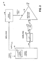
- FIG. 2 illustrates an amplification system or architecture 40 in accordance with another aspect of the present invention.
- the amplification system 40 switches operation between two or more voltage supply levels in response to a characteristic of an input signal relative to one or more threshold levels (e.g. , envelope amplitude level, digital count representation of signal level, power amplifier power level).
- a threshold level T 2 can be one or more fixed, selectable or programmable parameters associated with characteristics of the input signal.
- the amplification system 40 includes a digital control device 42, such as an application specific integrated circuit (ASIC), field programmable gate array (FPGA), a digital signal processor (DSP) or a combination of digital hardware and/or software components.
- the digital control device 42 includes a signal buffer 44 in which the input signal is stored prior to transmission through a signal path.
- the digital control device 42 controls a voltage level supplied by a DC/DC converter 58 via a supply control signal (SUPPLY CNTRL ) along a supply path.
- the DC/DC converter 58 provides a supply voltage that provides a voltage level to the supply and/or bias of the switching amplifier 56.
- the digital control device 42 provides one or more n-bit binary words 46 to a delta sigma modulator 48.
- the one or more n-bit binary words 46 represent an input signal that corresponds to a desired analog amplified output signal 60.
- the delta sigma modulator 48 converts the n-bit binary words 46 into a single bit binary waveform 50 having a square-like shape.
- the single bit binary waveform 50 is then provided to a one bit DAC 52, which transforms the single bit binary waveform 50 into the analog domain.
- An analog binary waveform 54 is then provided to the switching amplifier 56.
- the switching amplifier 56 includes inhibiting electronics, harmonic termination and/or zoning filters (not shown) that facilitate the reproduction of the desired amplified output signal within its desired spectrum.
- the amplitude and phase modulation of the output signal 60 is based on the pulse width modulation associated with the analog binary waveform 54.
- the output signal of the switching amplifier 56 can be a signal that conforms to WCDMA, multi-carrier GSM, OFDM or other signals having similar noise like signatures with high peak-to-average (PAR) ratios.
- the digital control device 42 determines the voltage supply level provided by the DC/DC converter 58 associated with the supply and/or bias voltage to the switching amplifier 56.
- the digital control device 42 determines the voltage supply level based on the threshold level T 2 and at least one characteristic associated with the input signal.
- the digital control device 42 examines the signal buffer 44 prior to transmission of the input signal to determine peak levels associated with the input signal.
- the digital control device 42 determines when to switch between a high voltage supply level for peak signals and a low voltage supply level for average signals.
- the delta sigma modulator 48 is employed to provide a signal similar to a pulse-width modulation signal where the signal varies between two voltage levels at very high rates (higher than the final average RF frequency of the wanted signal).
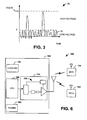
- FIG. 3 illustrates a graph 70 of voltage versus time of an exemplary input signal 72 of a switching amplifier prior to being converted to a binary form, in accordance with an aspect of the present invention.
- the threshold level T is selected to be an envelope amplitude voltage threshold level.
- the supply and/or bias voltage is set to a low voltage level.
- the supply and/or bias voltage is set to a high voltage level.
- Many communications signals, especially those using multiple carriers or CDMA formats, have very high but infrequent peaks.
- the output signal will have high efficiency when the signal is in the upper range (e.g., above T) but much lower efficiency for other input signals.
- the present invention overcomes this limitation, modifying the amplifier supply or bias in accordance with the input signal level.
- the threshold level is selected such that the envelope amplitude voltage level of the signal is below the amplitude threshold voltage level T substantially more often than the signal is above the envelope amplitude threshold voltage level T. Therefore, the amplification system will operate in the low supply voltage level substantially more often than at the high supply voltage level and consume less power and be more efficient.
- FIG. 4 illustrates an amplification system 100 that employs a two amplifier configuration (e.g. , similar to a Doherty amplifier configuration) in accordance with an aspect of the present invention.
- the amplification system 100 switches operation between a dual amplifier mode, and a single amplifier mode based on an envelope input signal amplitude level relative to a threshold level T 3 .
- the amplification system 100 includes a main amplifier 108 and a peak amplifier 112.
- the main amplifier 108 operates during average signal levels that are below the threshold level T 3 and both the main amplifier 108 and the peak amplifier 112 operate during peak signal levels that are above the threshold level T 3 .
- the peak amplifier 112 and the main amplifier 108 are switching amplifiers that amplify in response to a square wave like signal.
- the main amplifier 108 has a first voltage supply or bias (SUPPLY1), while the peak amplifier 112 has a second voltage supply or bias (SUPPLY2).
- the voltage level of the first voltage supply (SUPPLY1) and the second voltage supply (SUPPLY2) can be the same or different. It is to be appreciated that a different configuration can be employed if using a linear amplifier as the main amplifier 108. In the latter case the input to the main amplifier would not require conversion to a binary format.
- the amplification system 100 includes a digital control device 102.
- the digital control device 102 provides an input signal to a delta sigma modulator 104 along a signal path, provides a constant signal 109 to a switch device 110, and a switch control signal 111 to control the state of the switch device 110.
- the digital control device 102 provides one or more n-bit binary words 103 to a delta sigma modulator 104.
- the one or more n-bit binary words 103 represent an input signal that corresponds to a desired analog amplified output signal 118.
- the delta sigma modulator 104 converts the n-bit binary words 105 into a single bit binary waveform 105 having a square-like shape.
- the single bit binary waveform 105 is then provided to a one bit DAC 106, which transforms the single bit binary waveform 105 into the analog domain.
- An analog binary waveform 107 is provided to the main amplifier 108.
- the analog binary waveform 107 is also provided to the switch device 110.
- the digital control device 102 analyzes an input buffer (not shown) prior to transmission of the input signal to determine peak levels associated with the input signal. The digital control device 102 then determines when to switch the state of the switch device 110 via the switch control signal 111 based on peak signal levels and average signal levels of the input signal. For average signal levels, the zero-like input (e.g., constant signal) signal 109 is provided to the input of the peak amplifier 112 through the switch device 110. Since the peak amplifier 112 responds to an oscillating signal above a quiescent value of the peak amplifier 112, the peak amplifier 112 remains in an "OFF" state and does not consume power.
- the zero-like input (e.g., constant signal) signal 109 is provided to the input of the peak amplifier 112 through the switch device 110. Since the peak amplifier 112 responds to an oscillating signal above a quiescent value of the peak amplifier 112, the peak amplifier 112 remains in an "OFF" state and does not consume power.
- a control mechanism could set the supply level of the peak amplifier to a very low level, effectively turning it "OFF", thus eliminating the need for switch 110, switch control signal 111 and zero like signal 109.
- the analog binary signal 107 is provided to the peak amplifier input through the switch device 110 and to the main amplifier input.
- the outputs of the main amplifier 108 and the peak amplifier 112 are coupled together via a transmission line 114 and coupler 116.
- the output 118 of the amplification system 100 is a reconstructed amplified representation of the final composite signal, with contributions from both the main amplifier 108 and the peak amplifier 112.
- a zero-like input signal can be transmitted to the main amplifier and/or its supply level can be set to a very low level effectively turning it "OFF", thus eliminating the need for signal switching between the main amplifier 108 and the peak amplifier 108.
- the threshold level T 3 can be selected to achieve a desired efficiency, linearity and amplification system cost.
- the signal is provided to the main amplifier 108 substantially more often than the peak amplifier 112. Therefore, the amplification system can operate more efficiently than typical amplification systems employing signals with high peak-to-average ratios.
- the amplification systems illustrated in FIGS. 1 , 2 and 4 minimize the complexity of the circuitry necessary to amplify a given input signal by performing many of the functions that create variables in the amplification system in the digital domain. Additionally, the operation of the amplification system can be further improved by employing linearization techniques in the digital domain.
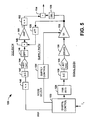
- FIG. 5 illustrates an amplification system 120 employing a linearization technique in accordance with an aspect of the present invention.
- the linearization technique is referred to as digital cross-cancellation.
- the digital cross-cancellation technique provides a digital reference of the wanted signal to a separate DAC generating a "clean" version of the wanted signal.
- the clean version of the wanted signal is inverted and combined with a portion of the output signal from the power amplifier to determine the unwanted portion of the output signal.
- the unwanted portion of the input signal is distortion and undesirable out-of band (OOB) emissions.
- OOB out-of band
- the present invention provides for generation of a clean reference signal or an inverted version of a clean reference signal in the digital domain.
- a digital control device 122 generates an input signal along a signal path, for example, an n-bit word representing an amplitude and phase modulated signal.
- the digital control device 122 determines the operating mode (e.g. , high supply voltage level, low supply voltage level) of the amplification system 120 based on a characteristic of the input signal, such as envelope amplitude, with respect to a threshold level T 4 .
- the digital control device 122 provides a mode select signal along a supply path to a supply control device 134, which controls the supply voltage and/or bias voltage to a switching amplifier 132.
- the supply voltage determines the supply level and/or bias level of the switching amplifier 132.
- the digital control device provides the input signal to a PAR reduction component 124.
- the PAR reduction component 124 can reduce peak signal levels through clipping or inclusion of the addition of signals.
- the PAR reduction component 124 then passes the PAR reduced n-bit input signal to a delta sigma modulator 126.
- the delta sigma modulator 126 converts the n-bit binary words into a single bit binary waveform having a square-like shape.
- the single bit binary waveform is then provided to a one bit DAC 128, which transforms the single bit binary waveform into the analog domain.
- the delta-sigma modulator 126 and the DAC 128 cooperate to perform a digital-to-analog conversion directly to radio transmission frequencies.
- the analog binary waveform is then provided to a driver or pre-amplifier 130, which provides additional gain to the analog binary waveform.
- the driver 130 provides the analog binary signal to the switching amplifier 132.
- the supply voltage level provided by the supply control 134 toggles between a high voltage level and a low voltage level to dynamically adjust the supply level and/or bias of the switching amplifier 132 in response to peak level signals associated with the input signal.
- the amplitude and phase modulation of the output signal of the amplification system 120 is based on the pulse width modulation associated with the analog binary waveform.
- the output signal of the amplification system 120 can be a signal that conforms to WCDMA, multi-carrier GSM, OFDM or other signals having similar noise like signatures with high peak-to-average (PAR) ratios.
- the digital control device 122 provides a reference signal along a DCC path to a digital inverter 140.
- the reference signal is a reference version (REF) of the input signal corresponding to the desired amplified output signal prior to any modifications.
- the digital inverter 140 can be eliminated and the inverted version of the clean reference signal can be provided by the digital control device 122.
- the inverted clean reference signal is transmitted to a delta-sigma modulator 142.
- the delta sigma modulator 142 is coupled to a DAC 144 and a band pass filter 146.
- the delta-sigma modulator 142, the DAC 144 and the band pass filter 146 cooperate to perform a digital-to-analog conversion directly to radio transmission frequencies of the inverted version of the clean reference signal (REF).
- a small portion of the output of the switch amplifier 132 is split off by a coupler through an attenuator 136 and summed with the inverted clean reference signal through a summer 148.
- the output of the summer 148 is signal distortion and OOB emissions.
- the output of the summer 148 is amplified by an error amplifier 150 to produce an error signal ( ⁇ ).
- the error signal is inverted through an inverter 152 to provide an inverted error signal.
- the inverted error signal is recombined with a delayed version (via delay device 138) of the output of the switching amplifier 132 through a summer 154 to remove OOB emissions and reduce distortion levels.
- the digital cross-cancellation technique in accordance with an aspect of the present invention can supply correction for amplifier distortions and it can correct spectral leakage into adjacent channels that occur. Additionally, since a digital clean reference signal is employed to determine the desired correction at the output, any modification of the signal can be corrected at the final output stage without the need for additional correction information during the amplification process.
- the amplification system of the present invention can be employed in a number of applications.
- the amplification system can be employed in wireless transmitter applications for base stations (e.g., satellites, cellular), handsets, and other mobile communication devices.
- FIG. 6 illustrates a communication system 180 having a base station 182 with a transmitter 184 employing a switching amplifier architecture 192 in accordance with an aspect of the present invention.
- the switching amplifier architecture 192 operates at a low voltage level when envelope amplitudes of transmission signals are below a threshold level and at a high voltage level when envelope amplitudes of transmission signals are above a threshold level.
- a central processing unit (CPU) 188 is coupled to the switching amplifier architecture system 192.
- the CPU 188 can facilitate control and threshold selection of the switching amplifier architecture system 192.
- the CPU 188 can generate the type of signal (e.g. , WCDMA, GSM, OFDM) to be transmitted and select the threshold level in which the switching amplifier architecture system 192 switches between high and low voltage supply levels.
- the base station 182 communicates to a group of mobile communication unit (MCUs) comprised of MCUs 194.
- the MCUs 194 are for illustrative purposes and it should be appreciated that the group of MCUs can include a greater number of MCUs based on the number of carriers in the output signal.
- the base station 182 also includes cooling devices 186 and power devices 190.
- the power devices 190 can include AC-DC power converters, fuses, battery backup devices that protect the base station 182 from power loss failures.
- the power devices 190 and cooling devices 186 can be substantially reduced in size and cost compared to conventional devices since the switching amplifier architecture 192 of the present invention operates with substantially more efficiency than conventional amplification systems.
- the base station 182 is illustrated as having a single transmitter 184, the base station 182 can have a plurality of transmitters communicating to different respective groups of MCUs over similar communication signal standards or different communication signal standards.
- the MCUs 194 can also include transmitters with switching amplifier architecture systems 192 that operate in a low voltage supply level and a high voltage supply level mode similar to that described for the transmitter 184.
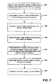
- FIG. 7 a methodology in accordance with various aspects of the present invention will be better appreciated with reference to FIG. 7 . While, for purposes of simplicity of explanation, the methodology of FIG. 7 is shown and described as executing serially, it is to be understood and appreciated that the present invention is not limited by the illustrated order, as some aspects could, in accordance with the present invention, occur in different orders and/or concurrently with other aspects from that shown and described herein. Moreover, not all illustrated features may be required to implement a methodology in accordance with an aspect the present invention.
- FIG. 7 illustrates a methodology for operating a switching amplification system in accordance with an aspect of the present invention.
- the methodology begins at 300 where one or more signal threshold levels and associated supply levels are selected.
- the threshold levels can be, for example, envelope amplitude levels in which a switching amplifier operates at one or more voltage supply levels for a corresponding envelope amplitude level range to modify voltage supply and/or bias associated with the switching amplification system to facilitate efficiency.
- a supply level adjustment profile is determined based on the input signal.
- the methodology then proceeds to 220.
- an input signal is converted into a single bit binary waveform. Peak signal levels of the input signal can be reduced through clipping or inclusion of the addition of signals prior to converting into the single bit binary waveform.
- the input signal can be an n-bit word that is delta sigma modulated into a single bit binary waveform.
- the single bit binary waveform is then converted from the digital to the analog domain at 230.
- the input signal is provide to the switching amplifier while the supply level and/or bias of the switching amplifier is dynamically adjusted based on the supply level adjustment profile.
- the supply level adjustment profile can change from a low voltage level for average level signals and a high voltage level for peak level signals.
- the supply level adjustment profile can be based on multi-supply levels, have a trapezoidal configuration or be a tracking waveform with adequate headroom to amplify the input signal.
- digital cross cancellation is performed on the output signal of the switching amplifier to linearize the output signal.
- the output signal is transmitted to a receiver.
- the output signal can be in a number of different single carrier or multi-carrier amplitude and phase modulated signal formats (e.g., WCDMA, GSM, OFDM).
Landscapes
- Engineering & Computer Science (AREA)
- Power Engineering (AREA)
- Amplifiers (AREA)
- Manipulation Of Pulses (AREA)
Claims (10)
- Verstärkerarchitektur (100), aufweisend:einen Schaltverstärker (132), der so wirkt, dass er ein Eingangssignal verstärkt;eine Versorgungssteuervorrichtung (134), die eine Versorgungsspannung des Schaltverstärkers (132) zwischen einer Vielzahl von festen Spannungsversorgungspegeln umschaltet, und zwar beruhend auf einer Eigenschaft des Eingangssignals relativ zu einem Schwellwertpegel; undeinen Binärwellenformwandler (18), der das Eingangssignal in eine binäre Wellenform zur Eingabe in den Schaltverstärker (132) umwandelt.
- Verstärkerarchitektur (100) nach Anspruch 1, ferner aufweisend einen Digital/Analog-Wandler, DAC, (144), der die binäre Wellenform in eine analoge Wellenform zum Verstärken durch den Schaltverstärker umwandelt.
- Verstärkerarchitektur (100) nach Anspruch 2, bei welcher der DAC einen ein-Bit-DAC (128) aufweist.
- Verstärkerarchitektur (100) nach Anspruch 1, bei der das Eingangssignal ein n-Bit-Wort ist, das ein phasen- und/oder amplitudenmoduliertes Signal darstellt und wobei der Schwellwertpegel ein Amplitudenhüllpegel ist, welcher der Eingangssignaldarstellung zugeordnet ist.
- Verstärkerarchitektur (100) nach Anspruch 4, bei welcher der Schaltverstärker ein Spitzenverstärker (112) ist, der in Kombination mit einem Hauptverstärker (108) konfiguriert ist, wobei der Spitzenverstärker (112) die binäre Wellenform für Eingangssignale oberhalb des Schwellwerts empfängt und der Spitzenverstärker für Eingangssignale unterhalb des Schwellwerts effektiv "AUS"-geschaltet ist.
- Verstärkerarchitektur (100) nach Anspruch 5, bei welcher der Hauptverstärker (108) die binäre Wellenform sowohl für Spitzensignale als auch für Durchschnittspegelsignale empfängt.
- Verstärkerarchitektur (100) nach Anspruch 5, bei welcher der Hauptverstärker für Eingangssignalpegel oberhalb des Schwellwerts effektiv "AUS"-geschaltet ist, und zwar entweder mittels Bereitstellens eines nullähnlichen Signals für den Eingang des Hauptverstärkers (108) oder mittels Einstellens des Versorgungspegels auf einen sehr niedrigen Pegel, der ihn für Eingangssignalpegel oberhalb des Schwellwerts effektiv "AUS"-schaltet.
- Verstärkerarchitektur (100) nach Anspruch 5, bei welcher der Spitzenverstärker (112) für Eingangssignalpegel unterhalb des Schwellwerts effektiv "AUS"-geschaltet ist, und zwar entweder mittels Bereitstellens eines nullähnlichen Signals für den Eingang des Spitzenverstärkers (112) oder mittels Einstellens des Versorgungspegels auf einen sehr niedrigen Pegel, der ihn für Eingangssignalpegel unterhalb des Schwellwerts effektiv "AUS"-schaltet.
- Verstärkungsarchitektur (100) nach Anspruch 1, ferner aufweisend eine digitale Steuervorrichtung (122), die das Eingangssignal analysiert und ein Spannungsversorgungspegel-Anpassungsprofil zum dynamischen Modifizieren der Versorgungsspannung an den Schaltverstärker (132) erstellt, und zwar als Reaktion auf Veränderungen in den Eigenschaften des Eingangssignals relativ zu dem Schwellwertpegel.
- Verstärkerarchitektur (100) nach Anspruch 1, bei welcher der Binärwellenformwandler einen Delta-Sigma-Modulator (132) aufweist.
Applications Claiming Priority (2)
| Application Number | Priority Date | Filing Date | Title |
|---|---|---|---|
| US10/691,987 US6982593B2 (en) | 2003-10-23 | 2003-10-23 | Switching amplifier architecture |
| US691987 | 2003-10-23 |
Publications (3)
| Publication Number | Publication Date |
|---|---|
| EP1536556A2 EP1536556A2 (de) | 2005-06-01 |
| EP1536556A3 EP1536556A3 (de) | 2005-08-31 |
| EP1536556B1 true EP1536556B1 (de) | 2011-06-29 |
Family
ID=34465626
Family Applications (1)
| Application Number | Title | Priority Date | Filing Date |
|---|---|---|---|
| EP04025039A Expired - Lifetime EP1536556B1 (de) | 2003-10-23 | 2004-10-21 | Schaltverstärkerarchitektur |
Country Status (2)
| Country | Link |
|---|---|
| US (1) | US6982593B2 (de) |
| EP (1) | EP1536556B1 (de) |
Cited By (2)
| Publication number | Priority date | Publication date | Assignee | Title |
|---|---|---|---|---|
| KR101097391B1 (ko) | 2010-10-04 | 2011-12-23 | 주식회사 피플웍스 | 비대칭 도허티 전력 증폭 장치의 입력 분배 및 제어 장치 |
| EP4014316A1 (de) * | 2019-08-14 | 2022-06-22 | Qorvo US, Inc. | Gerät zur verfolgung einer hüllkurve mit mehreren verstärkern |
Families Citing this family (43)
| Publication number | Priority date | Publication date | Assignee | Title |
|---|---|---|---|---|
| US7953174B2 (en) * | 2002-03-20 | 2011-05-31 | The Regents Of The University Of California | Radio transmission frequency digital signal generation |
| KR20050119197A (ko) * | 2003-04-07 | 2005-12-20 | 코닌클리즈케 필립스 일렉트로닉스 엔.브이. | 디지털 증폭기, 디지털 증폭기 시스템, 보상 회로 및 d형증폭기 동작 방법 |
| US20050201180A1 (en) * | 2004-03-05 | 2005-09-15 | Qualcomm Incorporated | System and methods for back-off and clipping control in wireless communication systems |
| US7355470B2 (en) | 2006-04-24 | 2008-04-08 | Parkervision, Inc. | Systems and methods of RF power transmission, modulation, and amplification, including embodiments for amplifier class transitioning |
| US7327803B2 (en) | 2004-10-22 | 2008-02-05 | Parkervision, Inc. | Systems and methods for vector power amplification |
| US7142053B2 (en) * | 2004-12-06 | 2006-11-28 | Skyworks Solutions, Inc. | Voltage clamp for improved transient performance of a collector voltage controlled power amplifier |
| JP4387936B2 (ja) * | 2004-12-13 | 2009-12-24 | 株式会社東芝 | 高周波用のドハティ型の高効率増幅器、およびその信号処理方法 |
| US7911272B2 (en) | 2007-06-19 | 2011-03-22 | Parkervision, Inc. | Systems and methods of RF power transmission, modulation, and amplification, including blended control embodiments |
| US20130078934A1 (en) | 2011-04-08 | 2013-03-28 | Gregory Rawlins | Systems and Methods of RF Power Transmission, Modulation, and Amplification |
| US8013675B2 (en) | 2007-06-19 | 2011-09-06 | Parkervision, Inc. | Combiner-less multiple input single output (MISO) amplification with blended control |
| US7248110B2 (en) * | 2005-12-06 | 2007-07-24 | Harris Corporation | Modified doherty amplifier |
| US7831221B2 (en) | 2005-12-13 | 2010-11-09 | Andrew Llc | Predistortion system and amplifier for addressing group delay modulation |
| US7761066B2 (en) * | 2006-01-27 | 2010-07-20 | Marvell World Trade Ltd. | Variable power adaptive transmitter |
| US7835710B2 (en) * | 2006-01-27 | 2010-11-16 | Marvell World Trade Ltd. | Variable power adaptive transmitter |
| CN101056289B (zh) * | 2006-01-27 | 2013-02-13 | 马维尔国际贸易有限公司 | 可变功率适应性发射器 |
| US8031804B2 (en) | 2006-04-24 | 2011-10-04 | Parkervision, Inc. | Systems and methods of RF tower transmission, modulation, and amplification, including embodiments for compensating for waveform distortion |
| US7937106B2 (en) | 2006-04-24 | 2011-05-03 | ParkerVision, Inc, | Systems and methods of RF power transmission, modulation, and amplification, including architectural embodiments of same |
| FI20065457A0 (fi) * | 2006-06-30 | 2006-06-30 | Nokia Corp | Tehovahvistimen kytkentätoimisen tehonsyötön kontrollointi |
| US8315336B2 (en) | 2007-05-18 | 2012-11-20 | Parkervision, Inc. | Systems and methods of RF power transmission, modulation, and amplification, including a switching stage embodiment |
| US8193860B2 (en) | 2006-11-21 | 2012-06-05 | Qualcomm, Incorporated | Method and apparatus for automatically controlling an XNN® enhancement circuitry feeding a power amplifier |
| US7620129B2 (en) | 2007-01-16 | 2009-11-17 | Parkervision, Inc. | RF power transmission, modulation, and amplification, including embodiments for generating vector modulation control signals |
| US7453384B2 (en) * | 2007-02-14 | 2008-11-18 | Analog Devices, Inc. | Digital to analog converter (DAC) circuit with extended operation range |
| JP2009005073A (ja) * | 2007-06-21 | 2009-01-08 | Nec Electronics Corp | デジタルアナログ変換器と歪補正回路 |
| WO2009005768A1 (en) | 2007-06-28 | 2009-01-08 | Parkervision, Inc. | Systems and methods of rf power transmission, modulation, and amplification |
| WO2009145887A1 (en) | 2008-05-27 | 2009-12-03 | Parkervision, Inc. | Systems and methods of rf power transmission, modulation, and amplification |
| US7619468B1 (en) * | 2008-09-30 | 2009-11-17 | Nortel Networks Limited | Doherty amplifier with drain bias supply modulation |
| US8462757B2 (en) * | 2008-12-15 | 2013-06-11 | Intel Mobile Communications GmbH | Method for adjusting transmitter output power |
| US8022768B1 (en) * | 2008-12-19 | 2011-09-20 | Nortel Networks Limited | Doherty amplifier and method for operation thereof |
| US8351542B2 (en) * | 2009-03-30 | 2013-01-08 | Texas Instruments Incorporated | Method and system for crest factor reduction |
| WO2011034975A2 (en) * | 2009-09-15 | 2011-03-24 | Miteq, Inc. | Measuring satellite linearity from earth using a low duty cycle pulsed microwave signal |
| EP2478732A4 (de) * | 2009-09-15 | 2017-07-26 | Miteq, Inc. | Verfahren zur übertragung höherer leistung von einem satelliten durch effizientere verwendung der existierenden satellitenleistungsverstärker |
| CN102761310B (zh) * | 2011-04-29 | 2015-06-10 | 中兴通讯股份有限公司 | 一种多合体功率放大器及其实现方法 |
| CN102158190A (zh) * | 2011-04-29 | 2011-08-17 | 中兴通讯股份有限公司 | 一种多合体功率放大器及其实现方法 |
| CN102185571A (zh) * | 2011-04-29 | 2011-09-14 | 中兴通讯股份有限公司 | 峰值放大器的导通控制方法、装置及多合体功率放大器 |
| CN102185568A (zh) * | 2011-04-29 | 2011-09-14 | 中兴通讯股份有限公司 | 一种多合体功率放大器及其实现方法 |
| KR20140034895A (ko) | 2011-06-02 | 2014-03-20 | 파커비전, 인크. | 안테나 제어 |
| US20130021104A1 (en) * | 2011-07-18 | 2013-01-24 | Ubidyne, Inc. | Amplifier arrangement |
| US8742843B2 (en) * | 2011-12-19 | 2014-06-03 | Intel Corporation | Power management in transceivers |
| JP2013192135A (ja) * | 2012-03-15 | 2013-09-26 | Panasonic Corp | ドハティ増幅器 |
| US9112649B2 (en) * | 2012-10-11 | 2015-08-18 | Qualcomm Incorporated | Method and apparatus for predicting signal characteristics for a nonlinear power amplifier |
| EP3047348B1 (de) | 2013-09-17 | 2025-03-19 | Parkervision, Inc. | Verfahren für die darstellung einer datenträgerzeitfunktion |
| WO2016131028A1 (en) * | 2015-02-15 | 2016-08-18 | Skyworks Solutions, Inc. | Doherty power amplifier having reduced size |
| IL263850B (en) * | 2018-12-19 | 2020-06-30 | Elbit Systems Land & C4I Ltd | System and method for compensating for ripple generated from a power supply |
Family Cites Families (4)
| Publication number | Priority date | Publication date | Assignee | Title |
|---|---|---|---|---|
| US6377784B2 (en) * | 1999-02-09 | 2002-04-23 | Tropian, Inc. | High-efficiency modulation RF amplifier |
| US6529716B1 (en) * | 2000-01-11 | 2003-03-04 | Skyworks Solutions, Inc. | RF transmitter with extended efficient power control range |
| US6472934B1 (en) * | 2000-12-29 | 2002-10-29 | Ericsson Inc. | Triple class E Doherty amplifier topology for high efficiency signal transmitters |
| US6987417B2 (en) * | 2003-06-24 | 2006-01-17 | Northrop Grumman Corpoation | Polar and linear amplifier system |
-
2003
- 2003-10-23 US US10/691,987 patent/US6982593B2/en not_active Expired - Lifetime
-
2004
- 2004-10-21 EP EP04025039A patent/EP1536556B1/de not_active Expired - Lifetime
Cited By (2)
| Publication number | Priority date | Publication date | Assignee | Title |
|---|---|---|---|---|
| KR101097391B1 (ko) | 2010-10-04 | 2011-12-23 | 주식회사 피플웍스 | 비대칭 도허티 전력 증폭 장치의 입력 분배 및 제어 장치 |
| EP4014316A1 (de) * | 2019-08-14 | 2022-06-22 | Qorvo US, Inc. | Gerät zur verfolgung einer hüllkurve mit mehreren verstärkern |
Also Published As
| Publication number | Publication date |
|---|---|
| US6982593B2 (en) | 2006-01-03 |
| EP1536556A2 (de) | 2005-06-01 |
| US20050088226A1 (en) | 2005-04-28 |
| EP1536556A3 (de) | 2005-08-31 |
Similar Documents
| Publication | Publication Date | Title |
|---|---|---|
| EP1536556B1 (de) | Schaltverstärkerarchitektur | |
| US7043213B2 (en) | Multi-mode amplifier system | |
| EP1492228B1 (de) | Verstärkerarchitektur für mehreren Betriebsarten | |
| US6987417B2 (en) | Polar and linear amplifier system | |
| US6998914B2 (en) | Multiple polar amplifier architecture | |
| US7034614B2 (en) | Modified polar amplifier architecture | |
| US7057455B2 (en) | System and method for reducing dynamic range and improving linearity in an amplication system | |
| EP1685646B1 (de) | Verstärkersystem mit variabler versorgung | |
| US7129778B2 (en) | Digital cross cancellation system | |
| US8254496B2 (en) | Power amplifier and radio wave transmitter having the same | |
| US7696818B2 (en) | Amplifying apparatus | |
| US20090088096A1 (en) | Apparatus and method for power amplification in wireless communication system | |
| KR101104143B1 (ko) | 무선 통신 시스템에서 신호의 송신 장치 및 방법 | |
| Sjöland et al. | Switched mode transmitter architectures | |
| Kim et al. | Digitally enhanced linear power amplifiers |
Legal Events
| Date | Code | Title | Description |
|---|---|---|---|
| PUAI | Public reference made under article 153(3) epc to a published international application that has entered the european phase |
Free format text: ORIGINAL CODE: 0009012 |
|
| AK | Designated contracting states |
Kind code of ref document: A2 Designated state(s): AT BE BG CH CY CZ DE DK EE ES FI FR GB GR HU IE IT LI LU MC NL PL PT RO SE SI SK TR |
|
| AX | Request for extension of the european patent |
Extension state: AL HR LT LV MK |
|
| PUAL | Search report despatched |
Free format text: ORIGINAL CODE: 0009013 |
|
| AK | Designated contracting states |
Kind code of ref document: A3 Designated state(s): AT BE BG CH CY CZ DE DK EE ES FI FR GB GR HU IE IT LI LU MC NL PL PT RO SE SI SK TR |
|
| AX | Request for extension of the european patent |
Extension state: AL HR LT LV MK |
|
| 17P | Request for examination filed |
Effective date: 20060112 |
|
| AKX | Designation fees paid |
Designated state(s): DE FI FR GB NL |
|
| 17Q | First examination report despatched |
Effective date: 20080714 |
|
| GRAP | Despatch of communication of intention to grant a patent |
Free format text: ORIGINAL CODE: EPIDOSNIGR1 |
|
| RAP1 | Party data changed (applicant data changed or rights of an application transferred) |
Owner name: NORTHROP GRUMMAN SYSTEMS CORPORATION |
|
| GRAS | Grant fee paid |
Free format text: ORIGINAL CODE: EPIDOSNIGR3 |
|
| GRAA | (expected) grant |
Free format text: ORIGINAL CODE: 0009210 |
|
| AK | Designated contracting states |
Kind code of ref document: B1 Designated state(s): DE FI FR GB NL |
|
| REG | Reference to a national code |
Ref country code: GB Ref legal event code: FG4D |
|
| REG | Reference to a national code |
Ref country code: DE Ref legal event code: R096 Ref document number: 602004033252 Country of ref document: DE Effective date: 20110818 |
|
| REG | Reference to a national code |
Ref country code: NL Ref legal event code: VDEP Effective date: 20110629 |
|
| PG25 | Lapsed in a contracting state [announced via postgrant information from national office to epo] |
Ref country code: NL Free format text: LAPSE BECAUSE OF FAILURE TO SUBMIT A TRANSLATION OF THE DESCRIPTION OR TO PAY THE FEE WITHIN THE PRESCRIBED TIME-LIMIT Effective date: 20110629 |
|
| PGFP | Annual fee paid to national office [announced via postgrant information from national office to epo] |
Ref country code: NL Payment date: 20111025 Year of fee payment: 8 |
|
| PLBE | No opposition filed within time limit |
Free format text: ORIGINAL CODE: 0009261 |
|
| STAA | Information on the status of an ep patent application or granted ep patent |
Free format text: STATUS: NO OPPOSITION FILED WITHIN TIME LIMIT |
|
| 26N | No opposition filed |
Effective date: 20120330 |
|
| REG | Reference to a national code |
Ref country code: DE Ref legal event code: R097 Ref document number: 602004033252 Country of ref document: DE Effective date: 20120330 |
|
| REG | Reference to a national code |
Ref country code: FR Ref legal event code: PLFP Year of fee payment: 12 |
|
| REG | Reference to a national code |
Ref country code: FR Ref legal event code: PLFP Year of fee payment: 13 |
|
| REG | Reference to a national code |
Ref country code: FR Ref legal event code: PLFP Year of fee payment: 14 |
|
| PGFP | Annual fee paid to national office [announced via postgrant information from national office to epo] |
Ref country code: DE Payment date: 20171019 Year of fee payment: 14 |
|
| REG | Reference to a national code |
Ref country code: FR Ref legal event code: PLFP Year of fee payment: 15 |
|
| REG | Reference to a national code |
Ref country code: DE Ref legal event code: R119 Ref document number: 602004033252 Country of ref document: DE |
|
| PG25 | Lapsed in a contracting state [announced via postgrant information from national office to epo] |
Ref country code: DE Free format text: LAPSE BECAUSE OF NON-PAYMENT OF DUE FEES Effective date: 20190501 |
|
| PGFP | Annual fee paid to national office [announced via postgrant information from national office to epo] |
Ref country code: FI Payment date: 20211021 Year of fee payment: 18 Ref country code: GB Payment date: 20211022 Year of fee payment: 18 |
|
| PGFP | Annual fee paid to national office [announced via postgrant information from national office to epo] |
Ref country code: FR Payment date: 20211021 Year of fee payment: 18 |
|
| GBPC | Gb: european patent ceased through non-payment of renewal fee |
Effective date: 20221021 |
|
| PG25 | Lapsed in a contracting state [announced via postgrant information from national office to epo] |
Ref country code: FR Free format text: LAPSE BECAUSE OF NON-PAYMENT OF DUE FEES Effective date: 20221031 |
|
| PG25 | Lapsed in a contracting state [announced via postgrant information from national office to epo] |
Ref country code: GB Free format text: LAPSE BECAUSE OF NON-PAYMENT OF DUE FEES Effective date: 20221021 |
|
| PG25 | Lapsed in a contracting state [announced via postgrant information from national office to epo] |
Ref country code: FI Free format text: LAPSE BECAUSE OF NON-PAYMENT OF DUE FEES Effective date: 20221021 |