EP1065856A2 - Basisbandvorverzerrungssystem für die linearisierung von Leistungsverstärker - Google Patents
Basisbandvorverzerrungssystem für die linearisierung von Leistungsverstärker Download PDFInfo
- Publication number
- EP1065856A2 EP1065856A2 EP00830422A EP00830422A EP1065856A2 EP 1065856 A2 EP1065856 A2 EP 1065856A2 EP 00830422 A EP00830422 A EP 00830422A EP 00830422 A EP00830422 A EP 00830422A EP 1065856 A2 EP1065856 A2 EP 1065856A2
- Authority
- EP
- European Patent Office
- Prior art keywords
- circuit
- clipping
- predistortion
- signal
- fact
- Prior art date
- Legal status (The legal status is an assumption and is not a legal conclusion. Google has not performed a legal analysis and makes no representation as to the accuracy of the status listed.)
- Withdrawn
Links
Images


Classifications
-
- H—ELECTRICITY
- H03—ELECTRONIC CIRCUITRY
- H03F—AMPLIFIERS
- H03F1/00—Details of amplifiers with only discharge tubes, only semiconductor devices or only unspecified devices as amplifying elements
- H03F1/32—Modifications of amplifiers to reduce non-linear distortion
- H03F1/3241—Modifications of amplifiers to reduce non-linear distortion using predistortion circuits
- H03F1/3282—Acting on the phase and the amplitude of the input signal
-
- H—ELECTRICITY
- H03—ELECTRONIC CIRCUITRY
- H03F—AMPLIFIERS
- H03F1/00—Details of amplifiers with only discharge tubes, only semiconductor devices or only unspecified devices as amplifying elements
- H03F1/32—Modifications of amplifiers to reduce non-linear distortion
- H03F1/3241—Modifications of amplifiers to reduce non-linear distortion using predistortion circuits
- H03F1/3247—Modifications of amplifiers to reduce non-linear distortion using predistortion circuits using feedback acting on predistortion circuits
-
- H—ELECTRICITY
- H03—ELECTRONIC CIRCUITRY
- H03F—AMPLIFIERS
- H03F1/00—Details of amplifiers with only discharge tubes, only semiconductor devices or only unspecified devices as amplifying elements
- H03F1/32—Modifications of amplifiers to reduce non-linear distortion
- H03F1/3241—Modifications of amplifiers to reduce non-linear distortion using predistortion circuits
- H03F1/3294—Acting on the real and imaginary components of the input signal
-
- H—ELECTRICITY
- H04—ELECTRIC COMMUNICATION TECHNIQUE
- H04L—TRANSMISSION OF DIGITAL INFORMATION, e.g. TELEGRAPHIC COMMUNICATION
- H04L27/00—Modulated-carrier systems
- H04L27/32—Carrier systems characterised by combinations of two or more of the types covered by groups H04L27/02, H04L27/10, H04L27/18 or H04L27/26
- H04L27/34—Amplitude- and phase-modulated carrier systems, e.g. quadrature-amplitude modulated carrier systems
- H04L27/36—Modulator circuits; Transmitter circuits
- H04L27/361—Modulation using a single or unspecified number of carriers, e.g. with separate stages of phase and amplitude modulation
-
- H—ELECTRICITY
- H04—ELECTRIC COMMUNICATION TECHNIQUE
- H04L—TRANSMISSION OF DIGITAL INFORMATION, e.g. TELEGRAPHIC COMMUNICATION
- H04L27/00—Modulated-carrier systems
- H04L27/32—Carrier systems characterised by combinations of two or more of the types covered by groups H04L27/02, H04L27/10, H04L27/18 or H04L27/26
- H04L27/34—Amplitude- and phase-modulated carrier systems, e.g. quadrature-amplitude modulated carrier systems
- H04L27/36—Modulator circuits; Transmitter circuits
- H04L27/366—Arrangements for compensating undesirable properties of the transmission path between the modulator and the demodulator
- H04L27/367—Arrangements for compensating undesirable properties of the transmission path between the modulator and the demodulator using predistortion
- H04L27/368—Arrangements for compensating undesirable properties of the transmission path between the modulator and the demodulator using predistortion adaptive predistortion
-
- H—ELECTRICITY
- H03—ELECTRONIC CIRCUITRY
- H03F—AMPLIFIERS
- H03F2200/00—Indexing scheme relating to amplifiers
- H03F2200/102—A non-specified detector of a signal envelope being used in an amplifying circuit
-
- H—ELECTRICITY
- H03—ELECTRONIC CIRCUITRY
- H03F—AMPLIFIERS
- H03F2200/00—Indexing scheme relating to amplifiers
- H03F2200/336—A I/Q, i.e. phase quadrature, modulator or demodulator being used in an amplifying circuit
-
- H—ELECTRICITY
- H03—ELECTRONIC CIRCUITRY
- H03F—AMPLIFIERS
- H03F2200/00—Indexing scheme relating to amplifiers
- H03F2200/438—Separate feedback of amplitude and phase signals being present
-
- H—ELECTRICITY
- H03—ELECTRONIC CIRCUITRY
- H03F—AMPLIFIERS
- H03F2200/00—Indexing scheme relating to amplifiers
- H03F2200/57—Separate feedback of real and complex signals being present
-
- H—ELECTRICITY
- H03—ELECTRONIC CIRCUITRY
- H03F—AMPLIFIERS
- H03F2200/00—Indexing scheme relating to amplifiers
- H03F2200/66—Clipping circuitry being present in an amplifier, i.e. the shape of the signal being modified
-
- H—ELECTRICITY
- H03—ELECTRONIC CIRCUITRY
- H03F—AMPLIFIERS
- H03F2201/00—Indexing scheme relating to details of amplifiers with only discharge tubes, only semiconductor devices or only unspecified devices as amplifying elements covered by H03F1/00
- H03F2201/32—Indexing scheme relating to modifications of amplifiers to reduce non-linear distortion
- H03F2201/3233—Adaptive predistortion using lookup table, e.g. memory, RAM, ROM, LUT, to generate the predistortion
-
- H—ELECTRICITY
- H04—ELECTRIC COMMUNICATION TECHNIQUE
- H04B—TRANSMISSION
- H04B1/00—Details of transmission systems, not covered by a single one of groups H04B3/00 - H04B13/00; Details of transmission systems not characterised by the medium used for transmission
- H04B1/02—Transmitters
- H04B1/04—Circuits
- H04B2001/0408—Circuits with power amplifiers
- H04B2001/0425—Circuits with power amplifiers with linearisation using predistortion
Definitions
- the present patent application for industrial invention concerns a predistortion system used to linearise amplifiers that exhibit non-linear distortion phenomena.
- An instantaneous non-linear amplifier can be generally modelled through its AM/AM and AM/PM distortion curves [1], [2].
- the spectral regrowth can be classified into the two following categories:
- Out-band intermodulations generate the interference between adjacent channels and can be filtered out at the amplifier output, although with a certain output power penalty due to filter insertion losses.
- Baseband predistortion is one of the known techniques used to counteract AM/AM and AM/PM distortions [2][3] and its digital adaptive implementation has been widely investigated in the last few years [4] [5] [6] [7].
- the aim of the present invention is to realise a predistortion system to linearise non linear amplifiers in such a way as to reduce the complexity and cost of, or even to eliminate, the amplifier output filters that are used to reduce the out-band spectral regrowth.
- the invention consists in combining the predistorting action with the signal pre-clipping in order to avoid or reduce both other clipping phenomena and the amplifier saturation, at the same allowing for filtering the out-band intermodulations produced by the clipping action itself.
- the object is achieved through the predistortion system according to the present invention, which includes a predistortion circuit, a clipping circuit to reduce the peak-to-mean power ratio of the signal and a device for filtering the spectral regrowth produced by the clipping circuit itself.
- pre-clipping is used to point out that the clipping operation has to be performed before predistortion.
- the second aim of the invention is to provide adaptation to the predistortion system.
- the second object is achieved by the present invention including both an input-output error circuit that provides the values to modify the action of the predistortion circuit and a timing circuit to synchronise the input to the output of the system in the predistortion system.
- the RF output of the ideally predistorted amplifier is equivalent to the RF modulation of a complex baseband signal, whose envelope is passed through a soft limiter device.
- the residual distortion introduced by the soft limiter depends on the signal peak-to-mean power ratio and on the input back off to the predistorted system (soft limiter).
- a residual distortion is introduced whenever the input back-off to the predistorted system is lower than the peak-to-mean power ratio of the signal.
- Distortions become as more evident as the input signal is characterised by a high peak-to-mean power ratio.
- the predistorted amplifier introduces some clipping on the signal envelope, the consequent spectral regrowth will degrade the signal both with respect to the signal-to-noise ratio and the adjacent channel interference.
- the only way to reduce the adjacent channel interference is to introduce an RF filter at the amplifier output.
- the present invention is characterised in that it realises clipping at baseband on the signal envelope, which is analogous to the one that would be introduced by the predistorted amplifier.
- post-clipping filters Such an approach allows for the baseband counteraction of the adjacent channel interference introduced by the clipping circuit itself by means of devices hereinafter defined as "post-clipping filters".
- the output of the post-clipping filters represents the baseband equivalent of the best residual distorted signal that can be obtained at the predistorted amplifier output.
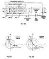
- Fig. 1(a) shows the scheme of an amplification system that makes use of a baseband Predistortion System (1), which combines the use of a Clipping and Interpolation Circuit (2) with a Predistortion Circuit (3).
- the amplification system scheme is exactly equivalent to the Quadrature modulation Circuit (9) that is positioned before the Predistorsion Circuit (3), as shown in Fig. 1(b).
- Fig. 2(a) shows the scheme of the Predistortion System (1) in which an Interpolation Circuit (4) is positioned before a Clipping Circuit (5), which in turn is positioned before the Predistortion Circuit (3).
- the Interpolation Circuit (4) can be realised by means of a Filling Circuit (4a) that inserts (N-1) zeros, or (N-1) replica of each sample between the signal input samples, with N being the interpolation factor.
- the real interpolation function is performed in cascade through the action of the Interpolation Filter Circuit (IFC) (4b).
- the signal that has been interpolated in such a way is elaborated by the Clipping Circuit (5) which firstly limits its maximum envelope (by means of the Clipping Device (5a)) and then eliminates the out-band spectral regrowth (by means of the Post Clipping Filters Circuit (PCF) (5b)).
- PCF Post Clipping Filters Circuit
- Fig. 2(b) shows a scheme of the Predistorsion System (1) that is an alternative to Fig. 2(a).
- an Interpolation & Clipping Circuit (2) firstly performs the Clipping action by means of the Clipping Device (5a), which is followed in cascade by a Filling Circuit (4a) that introduces zeros or input sample replica.
- the Filling Circuit (4a) is followed by the Filtering Circuit (4c) that simultaneously realises both the real interpolation filtering (IFC) and the post clipping filtering (PCF) of the signal outband spectral regrowth.
- IFC real interpolation filtering
- PCF post clipping filtering
- Fig. 3(a) and 3(b) graphically show the clipping operation performed by the Clipping Device (5a) on two general complex signals
- Fig. 3(b) and 3(a) represent the action of a Cartesian Clipping Device and the action of an Envelope Clipping Device, respectively.
- the first device separately cuts each one of the single components (V I , V Q ) over a certain value, while the second device jointly works on the single components (V I , V Q ) by cutting them in such a way that the envelope is lower than a certain threshold).
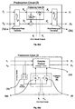
- Fig. 4(a) and 4(b) show two possible logical schemes to implement the base band Predistortion Circuit (3).
- the envelope R s ( t ) of this signal is used to address the Predistortion Table (6).
- the Predistortion Table (6) is organised in two Tables (6a) and (6b).
- the signal envelope R p ( t ) values of the Predistortion Circuit (3) output are memorised in Table (6b) while the predistortion phase values are memorised in Table (6b).
- the phase values will provide the predistortion signal phase values ⁇ p ( t ) after they have been added to the input signal phase ⁇ p ( t ).
- the envelope R p ( t ) and the phase ⁇ p ( t ) of the predistortion signal obtained in this way are elaborated by the Device (3b), which reconverts the predistortion signal into its Cartesian components p I ( t ) and p Q ( t ).
- Fig. 5 represents the conceptual scheme of an amplification system that includes the adaptation of a baseband predistortion system.
- the scheme includes the use of a Synchronisation Circuit (8) for the synchronisation of the Predistortion Circuit (3) input signal s & ( t ) with the RF amplifier output signal a & ( t ).
- a circuit (7) is also employed to determine the input-output error signal.
- Fig. 6 represents the logical scheme of a possible realisation of the Error Circuit (7) when the Predistortion Circuit (3) is realised according to the scheme in Fig. 4(a).
- the signal x & ( t ) in Fig.1 represents a complex digital signal at the input to the Predistortion System (1).
- the signal x & ( t ) can be eventually oversampled by the Interpolation Circuit (4) of Fig. 2(a) or by the Circuit (4a) of Fig. 2(b), if the input sample frequency is not high enough to correctly represent it in a non-linear environment.
- the Clipping Device (5a) shown in Fig. 2(a) or Fig. 2(b) limits the peak-to-mean power ratio of the signal in order to avoid or reduce any other clipping or saturation phenomenon that could be introduced by the Predistortion Circuit (3) and/or the RF Amplifier.
- the Clipping Device (5a) reduces the signal peak-to-mean power ratio constraining the envelope of the baseband signal inside a circle of the complex plane, as shown in Fig. 3(a), by a technique that is called Envelope Clipping.
- Cartesian Clipping reduces the signal envelope, but also introduces some extra phase distortion on the signal, as shown in Fig. 3(b).
- Cartesian Clipping is not exactly matched to the Envelope Clipping introduced by the predistorted amplifier.
- the predistorted amplifier will introduce further clipping if the complex signal clipping is realised outside to the square circumscribed to the amplifier clipping circle.
- unneeded extra distortions will be introduced by the Cartesian Clipping if the clipping square is inscribed into the amplifier clipping circle, as shown in Fig. 3 (b).
- the Clipping Circuit (5) that is placed after the interpolation circuit represents the best solution in terms of achievable performance.
- the output s & ( t ) of the Clipping & Interpolation Circuit (2) represents the input to the Predistortion Circuit (3).
- the Predistortion Circuit (3) modifies the complex signal components s I ( t ) and s Q ( t ) generating the components p I ( t ) and p Q ( t ) so as to introduce the AM/AM and AM/PM distortions that compensate for the ones introduced by the RF Amplifier.
- the Predistortion Circuit (3) shown in Fig. 4(a) is probably one of the most intuitive ones because it directly makes use of the AM/AM and AM/PM distortion curves.
- the Predistortion Circuit (3) shown in Fig. 4(b) uses a Complex Gain representation of the non-linear input-output characteristics.
- the second approach allows for working with Predistortion Tables (6a) and (6b) that are characterised by lower dimensions, even if the overall system complexity is increased.
- the Predistortion Circuit (3) may also adapt the distortion to be introduced, according to the changes of the working conditions caused by amplifier ageing, temperature variations, channel or power switching, and so on.
- the purpose of the Error Circuit (7) is to estimate the input-output non-linear error of the predistorted system and provide an error signal e & ( t ) to the Predistortion Circuit (3).
- Fig. 6 shows a possible implementation of the error circuit, where the envelope (a scaled replica) and the phase of the Predistortion Circuit (3) input s & ( t ) are subtracted from the correspondent amplifier output a & ( t ).
- the two error signals R e ( t ) and ⁇ e ( t ) obtained in this way are subsequently weighted by two real coefficients ⁇ R and ⁇ ⁇ in order to provide the correcting terms for the action of the Predistortion Circuit (3).
- the error signals are used as correcting term for the values memorised in Table (6a) and (6b) respectively, if the Predistortion Circuit is realised according to the scheme in Fig. 4(a).
- the algorithm has to be likewise implemented in Cartesian co-ordinates if the Predistortion System (1) makes use of the Predistortion Circuit (3) shown in Fig. 4(b).
- the magnitude of the adaptation coefficients ⁇ R and ⁇ ⁇ must be chosen as a compromise between adaptation speed and noise rejection.
- the purpose of the Synchronisation Circuit (8) is to estimate the loop delay of the adaptive system and compensate it in order to allow the Error Circuit (7) to correctly compare the input s & ( t ) of the Predistortion Circuit (3) with the output a & ( t ) of the amplifier.
Applications Claiming Priority (2)
| Application Number | Priority Date | Filing Date | Title |
|---|---|---|---|
| IT1999MC000051A IT1311679B1 (it) | 1999-06-17 | 1999-06-17 | Sistema di predistorsione per la linearizzazione di amplificatori. |
| ITMC990051 | 1999-06-17 |
Publications (2)
| Publication Number | Publication Date |
|---|---|
| EP1065856A2 true EP1065856A2 (de) | 2001-01-03 |
| EP1065856A3 EP1065856A3 (de) | 2003-09-03 |
Family
ID=11357712
Family Applications (1)
| Application Number | Title | Priority Date | Filing Date |
|---|---|---|---|
| EP00830422A Withdrawn EP1065856A3 (de) | 1999-06-17 | 2000-06-15 | Basisbandvorverzerrungssystem für die linearisierung von Leistungsverstärker |
Country Status (3)
| Country | Link |
|---|---|
| EP (1) | EP1065856A3 (de) |
| CA (1) | CA2311878A1 (de) |
| IT (1) | IT1311679B1 (de) |
Cited By (7)
| Publication number | Priority date | Publication date | Assignee | Title |
|---|---|---|---|---|
| EP1318600A2 (de) * | 2001-12-04 | 2003-06-11 | Nec Corporation | Verzerrungskompensationsschaltung zum Kompensieren von der in einem Leistungsverstärker auftretende Verzerrung |
| EP1501187A1 (de) * | 2003-07-23 | 2005-01-26 | Northrop Grumman Corporation | System und Verfahren zur Reduktion der Dynamik und Erhöhung der Linearität in einem Verstärkersystem |
| EP1614224A2 (de) * | 2003-04-16 | 2006-01-11 | Powerwave Technologies, Inc. | Additives digitales vorverzerrungssystem mit parallelwegkoordinatenumsetzung |
| WO2006114513A1 (fr) * | 2005-04-28 | 2006-11-02 | France Telecom | Procede de transmission d'un signal module avec une forte dynamique d'amplitude, emetteur et recepteur correspondant |
| WO2012003408A1 (en) * | 2010-06-30 | 2012-01-05 | Qualcomm Incorporated | Predistortion of complex modulated waveform |
| EP2541764A1 (de) * | 2011-06-30 | 2013-01-02 | Fujitsu Semiconductor Limited | System und Verfahren zur Schätzung und Korrektur von Phasenumtastung in einer drahtlosen Kommunikationsvorrichtung |
| US8964821B2 (en) | 2011-10-14 | 2015-02-24 | Qualcomm Incorporated | Shared feedback for adaptive transmitter pre-distortion |
Citations (4)
| Publication number | Priority date | Publication date | Assignee | Title |
|---|---|---|---|---|
| GB2315379A (en) * | 1996-07-11 | 1998-01-28 | Roke Manor Research | Reducing peak to average amplitude ratio in communication apparatus |
| US5737432A (en) * | 1996-11-18 | 1998-04-07 | Aphex Systems, Ltd. | Split-band clipper |
| EP0881807A1 (de) * | 1996-11-19 | 1998-12-02 | Matsushita Electric Industrial Co., Ltd | Sender |
| US5886573A (en) * | 1998-03-06 | 1999-03-23 | Fujant, Inc. | Amplification using amplitude reconstruction of amplitude and/or angle modulated carrier |
-
1999
- 1999-06-17 IT IT1999MC000051A patent/IT1311679B1/it active
-
2000
- 2000-06-15 EP EP00830422A patent/EP1065856A3/de not_active Withdrawn
- 2000-06-16 CA CA002311878A patent/CA2311878A1/en not_active Abandoned
Patent Citations (4)
| Publication number | Priority date | Publication date | Assignee | Title |
|---|---|---|---|---|
| GB2315379A (en) * | 1996-07-11 | 1998-01-28 | Roke Manor Research | Reducing peak to average amplitude ratio in communication apparatus |
| US5737432A (en) * | 1996-11-18 | 1998-04-07 | Aphex Systems, Ltd. | Split-band clipper |
| EP0881807A1 (de) * | 1996-11-19 | 1998-12-02 | Matsushita Electric Industrial Co., Ltd | Sender |
| US5886573A (en) * | 1998-03-06 | 1999-03-23 | Fujant, Inc. | Amplification using amplitude reconstruction of amplitude and/or angle modulated carrier |
Non-Patent Citations (1)
| Title |
|---|
| RUDGE P J ET AL: "Modelling spectral regrowth and the effect of packet size" HIGH FREQUENCY POSTGRADUATE STUDENT COLLOQUIUM, 1999 LEEDS, UK 17 SEPT. 1999, PISCATAWAY, NJ, USA,IEEE, US, 1999, pages 68-73, XP010361382 ISBN: 0-7803-5577-6 * |
Cited By (16)
| Publication number | Priority date | Publication date | Assignee | Title |
|---|---|---|---|---|
| EP1318600A2 (de) * | 2001-12-04 | 2003-06-11 | Nec Corporation | Verzerrungskompensationsschaltung zum Kompensieren von der in einem Leistungsverstärker auftretende Verzerrung |
| EP1318600A3 (de) * | 2001-12-04 | 2007-05-09 | Nec Corporation | Verzerrungskompensationsschaltung zum Kompensieren von der in einem Leistungsverstärker auftretende Verzerrung |
| EP1614224A2 (de) * | 2003-04-16 | 2006-01-11 | Powerwave Technologies, Inc. | Additives digitales vorverzerrungssystem mit parallelwegkoordinatenumsetzung |
| EP1614224A4 (de) * | 2003-04-16 | 2009-05-06 | Powerwave Technologies Inc | Additives digitales vorverzerrungssystem mit parallelwegkoordinatenumsetzung |
| EP1501187A1 (de) * | 2003-07-23 | 2005-01-26 | Northrop Grumman Corporation | System und Verfahren zur Reduktion der Dynamik und Erhöhung der Linearität in einem Verstärkersystem |
| US7042287B2 (en) | 2003-07-23 | 2006-05-09 | Northrop Grumman Corporation | System and method for reducing dynamic range and improving linearity in an amplication system |
| US7057455B2 (en) | 2003-07-23 | 2006-06-06 | Northrop Grumman Corporation | System and method for reducing dynamic range and improving linearity in an amplication system |
| WO2006114513A1 (fr) * | 2005-04-28 | 2006-11-02 | France Telecom | Procede de transmission d'un signal module avec une forte dynamique d'amplitude, emetteur et recepteur correspondant |
| WO2012003408A1 (en) * | 2010-06-30 | 2012-01-05 | Qualcomm Incorporated | Predistortion of complex modulated waveform |
| CN103039000A (zh) * | 2010-06-30 | 2013-04-10 | 高通股份有限公司 | 复合调制波形的预失真 |
| US8737526B2 (en) | 2010-06-30 | 2014-05-27 | Qualcomm Incorporated | Predistortion of complex modulated waveform |
| CN103039000B (zh) * | 2010-06-30 | 2015-11-25 | 高通股份有限公司 | 复合调制波形的预失真 |
| EP2541764A1 (de) * | 2011-06-30 | 2013-01-02 | Fujitsu Semiconductor Limited | System und Verfahren zur Schätzung und Korrektur von Phasenumtastung in einer drahtlosen Kommunikationsvorrichtung |
| JP2013017169A (ja) * | 2011-06-30 | 2013-01-24 | Fujitsu Semiconductor Ltd | 無線通信装置における位相シフトを推定及び補正するシステム及び方法 |
| US8891668B2 (en) | 2011-06-30 | 2014-11-18 | Intel IP Corporation | System and method for estimating and correcting phase shift in a wireless communication device |
| US8964821B2 (en) | 2011-10-14 | 2015-02-24 | Qualcomm Incorporated | Shared feedback for adaptive transmitter pre-distortion |
Also Published As
| Publication number | Publication date |
|---|---|
| ITMC990051A0 (it) | 1999-06-17 |
| EP1065856A3 (de) | 2003-09-03 |
| IT1311679B1 (it) | 2002-03-19 |
| CA2311878A1 (en) | 2000-12-17 |
| ITMC990051A1 (it) | 2000-12-17 |
Similar Documents
| Publication | Publication Date | Title |
|---|---|---|
| US10727879B2 (en) | Wide bandwidth digital predistortion system with reduced sampling rate | |
| US10728066B2 (en) | Modulation agnostic digital hybrid mode power amplifier system and method | |
| EP1738511B1 (de) | Verbessertes digitales Breitbandinjektionsvorverzerrungssystem und Verfahren | |
| EP1749359B1 (de) | Digitales Vorverzerrungssystem und Verfahren für hocheffiziente Sender | |
| US8903337B2 (en) | Multi-band wide band power amplifier digital predistortion system | |
| US6298097B1 (en) | Amplifier with wideband digital predistortion | |
| KR100448892B1 (ko) | 고전력 증폭기의 비선형 왜곡 보상을 위한 전치 왜곡 장치및 그 방법 | |
| US7068101B2 (en) | Adaptive predistortion for a transmit system | |
| US20030058959A1 (en) | Combined digital adaptive pre-distorter and pre-equalizer system for modems in link hopping radio networks | |
| US7251293B2 (en) | Digital pre-distortion for the linearization of power amplifiers with asymmetrical characteristics | |
| JPH03135249A (ja) | デジタル送信システム用先行歪ませ装置 | |
| EP1371202B1 (de) | Vorverzerrung zur korrektur von nichtlinearitäten sowie von gruppenlaufzeit bei satellitenkommunikation | |
| Bernardini et al. | Analysis of different optimization criteria for IF predistortion in digital radio links with nonlinear amplifiers | |
| EP1129556A1 (de) | Verfahren und vorrichtung zur verzerrungsverminderung digitaler daten | |
| EP1065856A2 (de) | Basisbandvorverzerrungssystem für die linearisierung von Leistungsverstärker | |
| Chang et al. | A compensation scheme for nonlinear distortion in OFDM systems | |
| EP1063825A2 (de) | Vorverzerrungssystem für die linearisierung von Leistungsverstärker | |
| Mahil et al. | Rational function based predistorter for traveling wave tube amplifiers | |
| KR20060098680A (ko) | 무선 통신 시스템에서 전력 증폭기의 기억 효과를 보상하는아날로그 전치 왜곡 장치 및 방법 | |
| Guo et al. | Post-compensation of RF non-linearity in mobile OFDM systems by estimation of memory-less polynomial | |
| Behravan et al. | Baseband compensation techniques for bandpass nonlinearities [RF front-ends] | |
| Levy et al. | Adaptation of a digital predistortion technique based on intersymbol interpolation | |
| Behravan et al. | Adaptive predistorter design for nonlinear high power amplifiers | |
| Baudoin et al. | A new adaptive base band predistortion algorithm for linearization of power amplifiers, application to EDGE-GSM transmitters |
Legal Events
| Date | Code | Title | Description |
|---|---|---|---|
| PUAI | Public reference made under article 153(3) epc to a published international application that has entered the european phase |
Free format text: ORIGINAL CODE: 0009012 |
|
| AK | Designated contracting states |
Kind code of ref document: A2 Designated state(s): AT BE CH CY DE DK ES FI FR GB GR IE IT LI LU MC NL PT SE |
|
| AX | Request for extension of the european patent |
Free format text: AL;LT;LV;MK;RO;SI |
|
| PUAL | Search report despatched |
Free format text: ORIGINAL CODE: 0009013 |
|
| AK | Designated contracting states |
Kind code of ref document: A3 Designated state(s): AT BE CH CY DE DK ES FI FR GB GR IE IT LI LU MC NL PT SE |
|
| AX | Request for extension of the european patent |
Extension state: AL LT LV MK RO SI |
|
| RIC1 | Information provided on ipc code assigned before grant |
Ipc: 7H 03F 1/32 B Ipc: 7H 04B 1/04 B Ipc: 7H 03F 3/32 B Ipc: 7H 04L 25/03 B Ipc: 7H 04L 27/36 A |
|
| AKX | Designation fees paid | ||
| STAA | Information on the status of an ep patent application or granted ep patent |
Free format text: STATUS: THE APPLICATION IS DEEMED TO BE WITHDRAWN |
|
| REG | Reference to a national code |
Ref country code: DE Ref legal event code: 8566 |
|
| 18D | Application deemed to be withdrawn |
Effective date: 20030701 |