EP1501162A2 - Phasengekoppelte Anordnung von Oxyd-isolierten VCSEL - Google Patents
Phasengekoppelte Anordnung von Oxyd-isolierten VCSEL Download PDFInfo
- Publication number
- EP1501162A2 EP1501162A2 EP04254333A EP04254333A EP1501162A2 EP 1501162 A2 EP1501162 A2 EP 1501162A2 EP 04254333 A EP04254333 A EP 04254333A EP 04254333 A EP04254333 A EP 04254333A EP 1501162 A2 EP1501162 A2 EP 1501162A2
- Authority
- EP
- European Patent Office
- Prior art keywords
- vcsel
- laser aperture
- oxide wall
- laser
- high gain
- Prior art date
- Legal status (The legal status is an assumption and is not a legal conclusion. Google has not performed a legal analysis and makes no representation as to the accuracy of the status listed.)
- Granted
Links
Images


Classifications
-
- H—ELECTRICITY
- H01—ELECTRIC ELEMENTS
- H01S—DEVICES USING THE PROCESS OF LIGHT AMPLIFICATION BY STIMULATED EMISSION OF RADIATION [LASER] TO AMPLIFY OR GENERATE LIGHT; DEVICES USING STIMULATED EMISSION OF ELECTROMAGNETIC RADIATION IN WAVE RANGES OTHER THAN OPTICAL
- H01S5/00—Semiconductor lasers
- H01S5/40—Arrangement of two or more semiconductor lasers, not provided for in groups H01S5/02 - H01S5/30
- H01S5/42—Arrays of surface emitting lasers
- H01S5/423—Arrays of surface emitting lasers having a vertical cavity
-
- H—ELECTRICITY
- H01—ELECTRIC ELEMENTS
- H01S—DEVICES USING THE PROCESS OF LIGHT AMPLIFICATION BY STIMULATED EMISSION OF RADIATION [LASER] TO AMPLIFY OR GENERATE LIGHT; DEVICES USING STIMULATED EMISSION OF ELECTROMAGNETIC RADIATION IN WAVE RANGES OTHER THAN OPTICAL
- H01S5/00—Semiconductor lasers
- H01S5/10—Construction or shape of the optical resonator, e.g. extended or external cavity, coupled cavities, bent-guide, varying width, thickness or composition of the active region
- H01S5/18—Surface-emitting [SE] lasers, e.g. having both horizontal and vertical cavities
- H01S5/183—Surface-emitting [SE] lasers, e.g. having both horizontal and vertical cavities having only vertical cavities, e.g. vertical cavity surface-emitting lasers [VCSEL]
- H01S5/18308—Surface-emitting [SE] lasers, e.g. having both horizontal and vertical cavities having only vertical cavities, e.g. vertical cavity surface-emitting lasers [VCSEL] having a special structure for lateral current or light confinement
- H01S5/18311—Surface-emitting [SE] lasers, e.g. having both horizontal and vertical cavities having only vertical cavities, e.g. vertical cavity surface-emitting lasers [VCSEL] having a special structure for lateral current or light confinement using selective oxidation
- H01S5/18313—Surface-emitting [SE] lasers, e.g. having both horizontal and vertical cavities having only vertical cavities, e.g. vertical cavity surface-emitting lasers [VCSEL] having a special structure for lateral current or light confinement using selective oxidation by oxidizing at least one of the DBR layers
-
- H—ELECTRICITY
- H01—ELECTRIC ELEMENTS
- H01S—DEVICES USING THE PROCESS OF LIGHT AMPLIFICATION BY STIMULATED EMISSION OF RADIATION [LASER] TO AMPLIFY OR GENERATE LIGHT; DEVICES USING STIMULATED EMISSION OF ELECTROMAGNETIC RADIATION IN WAVE RANGES OTHER THAN OPTICAL
- H01S5/00—Semiconductor lasers
- H01S5/10—Construction or shape of the optical resonator, e.g. extended or external cavity, coupled cavities, bent-guide, varying width, thickness or composition of the active region
- H01S5/18—Surface-emitting [SE] lasers, e.g. having both horizontal and vertical cavities
- H01S5/183—Surface-emitting [SE] lasers, e.g. having both horizontal and vertical cavities having only vertical cavities, e.g. vertical cavity surface-emitting lasers [VCSEL]
- H01S5/18308—Surface-emitting [SE] lasers, e.g. having both horizontal and vertical cavities having only vertical cavities, e.g. vertical cavity surface-emitting lasers [VCSEL] having a special structure for lateral current or light confinement
- H01S5/18338—Non-circular shape of the structure
Definitions
- VCSELs vertical cavity surface-emitting lasers
- One method of increasing the optic power at a target point is to align and simultaneously switch several lasers to form a composite beam.
- using an array of independent lasers results in each laser having its own independent intensity pattern.
- Combining independent intensity patterns results in a composite beam that appears as several distinct spots. These distinct spots are unsuitable for communications and printing applications where a central radiation lobe with a high concentration of power output is desired.
- the present invention relates generally to the field of laser fabrication. More particularly, a plurality of VCSELs are fabricated. A first VCSEL is at least partially surrounded by a first oxide wall and a second VCSEL is at least partially surrounded by a second oxide wall. A contact is structured to simultaneously provide power to both the first VCSEL and the second VCSEL.
- a high gain coupling region couples the active region of the first VCSEL to the active region of the second VCSEL through a gap in the first oxide wall and a corresponding gap in the second oxide wall. The high gain coupling region enhances mode coupling between the first VCSEL and the second VCSEL.
- the contact may provide current to the high gain coupling region.
- the gain of the high gain coupling region is higher than the gain of the first laser aperture.
- the contact may be formed from a transparent conductor and for example light output by the first laser aperture passes through the transparent conductor.
- the first laser aperture is completely surrounded by oxidized semiconductor material.
- an unoxidized opening in the first oxide wall bounding the first laser aperture coincides with a corresponding opening in the second oxide wall bounding the second laser aperture such that during operation, electromagnetic radiation from the first laser couples to the second laser inducing mode coupling between the first laser and the second laser.
- the first and/or second oxide wall bounding the first laser aperture may include a plurality of via holes, the first oxide wall formed by lateral oxidation from the plurality of via holes.
- the first oxide wall and the second oxide wall may merge together in a section, the merged together section separating the first laser aperture from the second laser aperture.
- a third VCSEL may be positioned adjacent to the first VCSEL, the third VCSEL including a third laser aperture partially surrounded by a third oxide wall and an opening in the third oxide wall, a second opening in the first oxide wall and the opening in the third oxide wall aligned to allow evanescent waves from the first VCSEL to reach an active region of the third VCSEL.
- the single contact may simultaneously provide power to the first VCSEL, the second VCSEL and the third VCSEL.
- a high gain coupling region may be provided formed by heavily doping the substrate in the at least one opening in the first oxide wall and the corresponding opening in the second oxide wall.
- the array may further comprise:
- a high loss region may be formed over the high gain region, when provided, to decrease cavity quality factor and increase the threshold for lasing.
- the high loss region may be formed by heavy p type doping in a mirror layer over the high gain region.
- a common contact addresses several VCSELs simultaneously.
- the VCSELs will be closely spaced and separated by thin, laterally oxidized regions designed to promote mode leakage between adjacent VCSELs. The mode leakage keeps the output of adjacent VCSELs in phase thereby allowing the output of these adjacent VCSELs to be combined into a coherent composite beam.
- Figure 1 shows a cross-sectional side view of an oxide-confined VCSEL mesa-structure with an etched pillar structure.
- Mesa sidewalls 104 provide access to buried aluminum-containing layers 108.
- Buried layer 108 is selectively oxidized to form laser apertures 112, 116, 120.
- the edge of the mesa completely surrounds the laser aperture such that an air gap 124 completely separates adjacent laser apertures 112 and 116. The air gap prevents close coupling of optical fields between adjacent lasers.
- via holes instead of pillars to access the oxidation layers allows much tighter packing of VCSEL structures.
- the via holes are typically arranged along the corners of a polygon such that upon oxidation, the oxidation fronts originating from each via hole expands and merges with oxidation fronts from adjacent via holes to define a laser aperture at the center of the polygon.
- Figure 2 shows a top view micrograph of four laser apertures 204, 208, 212, 216.
- Figure 3 illustrates adjacent laser aperture regions such as region 304, 308 that share different sections of an oxidation front generated by a common via hole 312. Sharing the oxidation front generated by each via hole increases VCSEL density in a unit area and further enhances mode coupling between neighboring VCSELs. Ideally, sufficient mode coupling induces mode locking between adjacent aperture regions.
- Figure 3 shows a 64 VCSEL element structure arranged in an 8x8 rectangular array.
- a transparent indium tin oxide (ITO) electrode 316 covers the entire array.
- Contacts 320 couple the ITO electrode to a power supply (not shown). The ITO electrode provides an injection current to the laser apertures.
- ITO indium tin oxide
- An oxidized material at least partially surrounds each VCSEL in the array.
- the oxidized material forms a lateral waveguide defining an optical aperture.
- Limiting the extent of lateral oxidation enhances mode leakage and coupling between adjacent VCSEL laser apertures.
- the oxidation extent 314, defined to be the shortest distance from the edge of the via hole to the edge of the oxidation should preferably be less than 0.5 micrometers.
- a typical oxidation time for Al 0.8 Ga 0.2 As is approximately 7 minutes.
- the actual spacing between adjacent oxidation fronts defining a laser aperture varies according to a number of factors including the wavelength output by the laser and the effective refractive index within the aperture.
- the extent of the evanescent wave that induces mode locking determines the spacing of via holes and the oxidation times.
- the electromagnetic field strength of an evanescent wave typically decreases as a function of e -z/zo where z is the distance from the boundary of the aperture and zo is a characteristic length.
- This characteristic length is approximately equal to the wavelength of the laser divided by 2pi(sqrt(2(n*f*dn))) where n is the effective refractive index of the aperture, f is the fraction of the oxidized to unoxidized area in the coupling region between array elements, and dn is the effective refractive reduction in the oxidized region.
- a typical VCSEL operates around 850 nm, the effective index of refraction n is approximately 3, and an example effective refractive reduction dn is approximately 0.065.
- the characteristic length z o is approximately 0.87 micrometers.
- a mode interaction length may be computed. The mode interaction length is typically assumed to be approximately five times the characteristic length. However, the mode interaction length may be extended up to approximately ten times the characteristic length by further distancing the oxidation epitaxial layer 150 of Figure 1 further from the laser active regions 154. Using such parameters, the laser dimensions are adjusted to allow for mode locking between adjacent lasers.
- a laser phase array usually operates in higher order supermodes producing two or more radiation lobes existing in the far field.
- single mode operation that concentrates light power in a single radiation lobe is desirable for many applications.
- one embodiment of the invention blocks or otherwise diminishes the unwanted far field lobes.
- An alternative embodiment of the invention achieves fundamental supermode operation (with a single radiation lobe in the far field region) by positioning high gain coupling regions between adjacent laser apertures. These high gain coupling regions may have higher gains than the gain found in the actual laser aperture.
- One method of increasing gain is to increase the conductivity of the coupling regions compared to the conductivity of the laser aperture regions. Higher conductivity increases the current density (more current per unit area) in the high gain coupling regions compared to the laser aperture regions.
- One method of increasing the conductivity is to dope the high gain coupling region with a suitable dopant such as zinc.
- the doping may be done by masking the laser aperture regions and diffusing a suitable dopant into the coupling region.
- the dopant may be added by direct ion implantation.
- the mirror reflectivity over the coupling region may be reduced. This reduction can be accomplished by, for example, eliminating part or all of the upper mirror layers above the coupling region.
- VCSEL wafers can be masked so that upper DBR mirrors in unprotected areas above the coupling region can be selectively etched by, for example, chemically-assisted ion beam etching.
- a second method of reducing reflectivity of mirrors above the high gain coupling region is to deposit additional thin film layers on that region. These additional layers reduce reflectivity if they are not specifically designed to phase match the existing mirror layers. Efficient reflectivity reduction occurs when the additional layers are specifically designed as antireflection coatings to negate the reflectivity of the DBR layers.
- Still a third method of preventing lasing in the high gain coupling region is to selectively introduce optical loss either in the coupling region itself or in the mirrors above the coupling region.
- optical loss For example, heavy p-type doping in the mirror layers, near the active light-emitting layers enhances free carrier absorption. The higher optical loss decreases cavity quality factor and increases the threshold for lasing in those areas.
- Figure 4 is a flow chart that describes one method of fabricating a VCSEL laser phase array.
- a VCSEL epi-structure is grown.
- An example structure typically includes an n-doped DBR (distributed Bragg reflector stack) followed by an active layer and a p-doped DBR on a substrate.
- the active layer allows selective oxidation, typically by including a high Al-content in the active layer regions to be oxidized.
- Block 408 describes forming high gain coupling regions between apertures. Formation of these coupling regions encourages fundamental supermode operation.
- one method of forming the high gain coupling region includes diffusing a p-dopant such as zinc to increase the conductivity of the coupling region.
- Masks overlaying the laser aperture controls diffusion of the p-dopant into the coupling region.
- these same masks may be used to allow selective etching of the mirrors above the high gain coupling region as described in block 410. The selective etching reduces mirror reflectivity and prevent lasing in the coupling regions. After use, the masks may be removed.
- a transparent electrode is deposited over the wafer surface.
- a sputtering process is used to deposit indium tin oxide (ITO) or Zinc Oxide to form a transparent electrode.
- ITO indium tin oxide
- the transparent electrode simultaneously provides current to several adjacent lasers in the laser array.
- the transparent electrode may also overlay the high gain coupling regions to provide current, and thus optical gain, into the coupling regions.
- the transparent electrode forms a "blanket" over the entire laser array uniformly injecting current while simultaneously allowing high light output through the transparent electrode. Adjusting the thickness of the transparent electrode to one half the wavelength of light output by the laser array minimizes light reflections by the electrode.
- successive rapid anneals may be performed.
- a first anneal crystallizes the sputtered transparent electrode material.
- a second anneal forms an ohmic contact between the transparent electrode and the underlying GaAs material.
- a lattice of via holes are patterned.
- via holes are etched.
- a dry etch is used to etch through the transparent electrode and the underlying epi layers exposing the buried oxidizable layer, typically a high aluminum content AlGaAs layer near the active region.
- the via holes are arranged such that each set of via holes form the verticies of a polygon surrounding each laser aperture.
- the laser array is placed in a wet oxidation furnace to laterally oxidize the buried layer through the via holes as described in block 420.
- the time and temperature of the oxidation process depends on the oxidation extent. Limiting the oxidation time prevents an oxidation region originating from a via hole from contacting an adjacent oxidation region originating from an adjacent via hole.
- the unoxidized region remaining between adjacent oxidized regions serves as the high gain coupling regions between adjacent laser apertures.
- the oxidation regions form the lateral waveguide array.
- metal contacts are attached. These metal contacts couple the transparent electrode to a power source.
- ion implantation creates insulating regions between adjacent sub-units. Each sub-unit serves as an independently addressable set of phase array lasers. The ion implantation may use a variety of elements such as hydrogen.
- a second electrode is attached to the phase array of lasers.
- the second electrode is an n-contact metal deposited on the wafer backside.
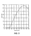
- Figure 5 shows a room temperature CW light output versus input current curve of a typical 64 element array of VCSELs. Proper heat sinking of the VCSEL array allows generation of significantly higher light output levels at a given current level.
- Figure 3 shows a laterally oxidized 8x8 VCSEL phase array structure formed using a hexagonal arrangements of via holes
- Figure 6 shows a higher density of VCSELs formed by using a square or grid arrangement of via holes.
- Each set of four via holes such as via holes 604, 608, 612, 616 form the verticies of a square polygon that surrounds laser aperture 620.
- a laterally oxidized region such as laterally oxidized region 624, surrounds each via hole such as via hole 604.
- the oxidized region forms the edge of the waveguide surrounding laser aperture 620.
- the laterally oxidized regions are made small in extent such that a gap or coupling region 628 exists between adjacent laterally oxidized regions.
- the coupling region allows mode coupling between adjacent laser apertures such as laser aperture 620 and laser aperture 632.
- Figure 7 shows an alternative, compact arrangement of a laterally oxidized 8x8 VCSEL phase array design that utilizes a triangular device geometry.
- three via holes, such as via holes 704, 708, 712 form the verticies of a triangle polygon that surrounds a corresponding laser aperture such as laser aperture 716.
- a laterally oxidized region, such as oxidized region 720 surrounds each via hole.
- the laterally oxidized regions form a waveguide for each laser aperture.
- adjacent oxidized regions contact, for example oxidized region 820 contacts oxidized region 824, resulting in reduced mode coupling between adjacent laser apertures.
- Figure 8 shows a structure similar to the structure of Figure 7 except that high gain regions such as high gain region 828 separate adjacent oxidized regions, such as oxidized regions 820 and 824.
- each oxidized region includes only one corresponding via hole such that high gain regions and laser apertures completely surround each oxidized region.
- an oxidized region originating from a first via hole does not contact an adjacent oxidized region originating from an adjacent via hole.
- the high gain region, such as high gain region 828 couples adjacent laser apertures and allows significant mode coupling between adjacent laser apertures, such as laser apertures 832 and 836.
Landscapes
- Physics & Mathematics (AREA)
- Condensed Matter Physics & Semiconductors (AREA)
- General Physics & Mathematics (AREA)
- Electromagnetism (AREA)
- Optics & Photonics (AREA)
- Semiconductor Lasers (AREA)
Applications Claiming Priority (2)
| Application Number | Priority Date | Filing Date | Title |
|---|---|---|---|
| US625811 | 1996-03-29 | ||
| US10/625,811 US7257141B2 (en) | 2003-07-23 | 2003-07-23 | Phase array oxide-confined VCSELs |
Publications (3)
| Publication Number | Publication Date |
|---|---|
| EP1501162A2 true EP1501162A2 (de) | 2005-01-26 |
| EP1501162A3 EP1501162A3 (de) | 2005-12-28 |
| EP1501162B1 EP1501162B1 (de) | 2010-09-15 |
Family
ID=33490887
Family Applications (1)
| Application Number | Title | Priority Date | Filing Date |
|---|---|---|---|
| EP04254333A Expired - Lifetime EP1501162B1 (de) | 2003-07-23 | 2004-07-20 | Phasengekoppelte Anordnung von VCSELs mit Oxid-Begrenzung |
Country Status (4)
| Country | Link |
|---|---|
| US (1) | US7257141B2 (de) |
| EP (1) | EP1501162B1 (de) |
| JP (1) | JP2005045243A (de) |
| DE (1) | DE602004029122D1 (de) |
Cited By (12)
| Publication number | Priority date | Publication date | Assignee | Title |
|---|---|---|---|---|
| EP2070058A1 (de) * | 2006-09-27 | 2009-06-17 | Giesecke & Devrient GmbH | Vorrichtung und verfahren zur optischen untersuchung von wertdocumenten |
| CN102136538A (zh) * | 2010-01-21 | 2011-07-27 | Lg伊诺特有限公司 | 发光器件及其制造方法、发光器件封装以及照明系统 |
| WO2016027105A1 (en) * | 2014-08-22 | 2016-02-25 | The University Of Sheffield | Improved laser structure |
| EP3329562A4 (de) * | 2015-07-30 | 2019-04-17 | Optipulse Inc. | Starre hochleistungs- und hochgeschwindigkeitslaserrasterstrukturen |
| WO2020061752A1 (en) * | 2018-09-25 | 2020-04-02 | Shenzhen Raysees Technology Co., Ltd. | Vertical Cavity Surface Emitting Laser (VCSEL) Array and Manufacturing Method |
| US10630053B2 (en) | 2015-07-30 | 2020-04-21 | Optipulse Inc. | High power laser grid structure |
| CN111699598A (zh) * | 2017-12-08 | 2020-09-22 | 通快光电器件有限公司 | 分段垂直腔面发射激光器 |
| US10868616B2 (en) | 2017-09-06 | 2020-12-15 | Optipulse Inc. | Method and apparatus for alignment of a line-of-sight communications link |
| US10958350B2 (en) | 2017-08-11 | 2021-03-23 | Optipulse Inc. | Laser grid structures for wireless high speed data transfers |
| EP3961830A1 (de) * | 2020-08-24 | 2022-03-02 | Changchun Institute of Optics, Fine Mechanics and Physics, Chinese Academy of Sciences | Strahlungsemitter |
| WO2024017891A1 (en) * | 2022-07-19 | 2024-01-25 | Powerphotonic Ltd | Coherent beam combination method and apparatus |
| US11936163B2 (en) | 2020-08-24 | 2024-03-19 | Changchun Institute Of Optics, Fine Mechanics And Physics | Radiation emitter |
Families Citing this family (60)
| Publication number | Priority date | Publication date | Assignee | Title |
|---|---|---|---|---|
| JP2005142463A (ja) * | 2003-11-10 | 2005-06-02 | Sony Corp | 半導体発光素子およびその製造方法 |
| DE102005016592A1 (de) * | 2004-04-14 | 2005-11-24 | Osram Opto Semiconductors Gmbh | Leuchtdiodenchip |
| JP4784123B2 (ja) * | 2005-03-28 | 2011-10-05 | 富士ゼロックス株式会社 | マルチスポット型面発光レーザおよびその製造方法 |
| KR100696207B1 (ko) * | 2005-04-14 | 2007-03-20 | 엔에이치엔(주) | 조커를 이용한 카드 게임 서비스 제공 방법 및 이를 위한기록 매체 |
| WO2007116659A1 (ja) | 2006-03-23 | 2007-10-18 | Nec Corporation | 面発光レーザ |
| CN100456584C (zh) * | 2006-08-02 | 2009-01-28 | 长春理工大学 | 大出光孔垂直腔面发射半导体激光器的多芯电注入结构 |
| JP2008041937A (ja) * | 2006-08-07 | 2008-02-21 | Yokogawa Electric Corp | 面発光レーザ |
| JP2008177430A (ja) * | 2007-01-19 | 2008-07-31 | Sony Corp | 発光素子及びその製造方法、並びに、発光素子集合体及びその製造方法 |
| US10038304B2 (en) | 2009-02-17 | 2018-07-31 | Trilumina Corp. | Laser arrays for variable optical properties |
| US8995493B2 (en) | 2009-02-17 | 2015-03-31 | Trilumina Corp. | Microlenses for multibeam arrays of optoelectronic devices for high frequency operation |
| US20130223846A1 (en) | 2009-02-17 | 2013-08-29 | Trilumina Corporation | High speed free-space optical communications |
| US7949024B2 (en) * | 2009-02-17 | 2011-05-24 | Trilumina Corporation | Multibeam arrays of optoelectronic devices for high frequency operation |
| US10244181B2 (en) | 2009-02-17 | 2019-03-26 | Trilumina Corp. | Compact multi-zone infrared laser illuminator |
| US8995485B2 (en) | 2009-02-17 | 2015-03-31 | Trilumina Corp. | High brightness pulsed VCSEL sources |
| KR101731249B1 (ko) | 2009-08-20 | 2017-04-28 | 코닌클리케 필립스 엔.브이. | 각도-선택 피드백을 갖는 수직 캐비티 표면 방출 레이저 디바이스 |
| US8537874B2 (en) * | 2010-10-28 | 2013-09-17 | Flir Systems, Inc. | High fill-factor efficient vertical-cavity surface emitting laser arrays |
| US11095365B2 (en) | 2011-08-26 | 2021-08-17 | Lumentum Operations Llc | Wide-angle illuminator module |
| US9372308B1 (en) | 2012-06-17 | 2016-06-21 | Pacific Biosciences Of California, Inc. | Arrays of integrated analytical devices and methods for production |
| US9624540B2 (en) | 2013-02-22 | 2017-04-18 | Pacific Biosciences Of California, Inc. | Integrated illumination of optical analytical devices |
| JP6339665B2 (ja) * | 2013-04-22 | 2018-06-06 | トリルミナ コーポレーション | 高周波動作のための光電子装置のマルチビームアレイ用マイクロレンズ |
| JP6240429B2 (ja) | 2013-08-07 | 2017-11-29 | 国立大学法人東京工業大学 | 面発光型半導体レーザおよび光伝送装置 |
| US9520696B2 (en) | 2014-03-04 | 2016-12-13 | Princeton Optronics Inc. | Processes for making reliable VCSEL devices and VCSEL arrays |
| TWI692633B (zh) | 2014-08-27 | 2020-05-01 | 美商加州太平洋生物科學公司 | 整合式分析裝置之陣列 |
| EP3271762B1 (de) | 2015-03-16 | 2023-01-04 | Pacific Biosciences of California, Inc. | Analysesystem umfassend integrierte vorrichtungen und systeme zur optischen freiraumkopplung |
| EP3292220B1 (de) | 2015-05-07 | 2022-07-13 | Pacific Biosciences of California, Inc. | Multiprozessor-pipeline-architektur |
| EP4425153A3 (de) | 2015-06-12 | 2024-11-20 | Pacific Biosciences Of California, Inc. | Integrierte zielwellenleitervorrichtungen und systeme zur optischen kopplung |
| US9742153B1 (en) * | 2016-02-23 | 2017-08-22 | Lumentum Operations Llc | Compact emitter design for a vertical-cavity surface-emitting laser |
| US10250012B2 (en) | 2016-06-02 | 2019-04-02 | Lumentum Operations Llc | Variable emission area design for a vertical-cavity surface-emitting laser array |
| US10116115B2 (en) | 2017-02-22 | 2018-10-30 | Geoff W. Taylor | Integrated circuit implementing a VCSEL array or VCSEL device |
| DE102017108104A1 (de) * | 2017-04-13 | 2018-10-18 | Osram Opto Semiconductors Gmbh | Oberflächenemittierender Halbleiterlaser und Verfahren zu dessen Herstellung |
| US10153614B1 (en) * | 2017-08-31 | 2018-12-11 | Apple Inc. | Creating arbitrary patterns on a 2-D uniform grid VCSEL array |
| US10355456B2 (en) * | 2017-09-26 | 2019-07-16 | Lumentum Operations Llc | Emitter array with variable spacing between adjacent emitters |
| US10205303B1 (en) | 2017-10-18 | 2019-02-12 | Lumentum Operations Llc | Vertical-cavity surface-emitting laser thin wafer bowing control |
| US11283240B2 (en) * | 2018-01-09 | 2022-03-22 | Oepic Semiconductors, Inc. | Pillar confined backside emitting VCSEL |
| US10720758B2 (en) | 2018-03-28 | 2020-07-21 | Lumentum Operations Llc | Emitter array with shared via to an ohmic metal shared between adjacent emitters |
| US11522344B2 (en) * | 2018-03-28 | 2022-12-06 | Lumentum Operations Llc | Optimizing a layout of an emitter array |
| KR102171733B1 (ko) * | 2018-04-02 | 2020-10-29 | 주식회사 레이아이알 | 수직 공동 표면 방출 레이저 |
| US11178392B2 (en) * | 2018-09-12 | 2021-11-16 | Apple Inc. | Integrated optical emitters and applications thereof |
| CN113557644B (zh) | 2019-02-04 | 2024-03-29 | 苹果公司 | 具有一体式微透镜的竖直发射器 |
| WO2020224811A1 (en) * | 2019-05-09 | 2020-11-12 | Lumileds Holding B.V. | Light-emitting device |
| WO2021007771A1 (en) | 2019-07-16 | 2021-01-21 | 3M Innovative Properties Company | Optical transceiver module |
| US12535420B2 (en) | 2020-02-18 | 2026-01-27 | Pacific Biosciences Of California, Inc. | Highly multiplexed nucleic acid sequencing systems |
| CN115516721A (zh) | 2020-05-10 | 2022-12-23 | 苹果公司 | 折叠的光学共轭透镜 |
| US11855413B2 (en) | 2020-06-22 | 2023-12-26 | Lumentum Operations Llc | Vertical-cavity surface-emitting laser array with isolated cathodes and a common anode |
| US11302352B2 (en) | 2020-06-22 | 2022-04-12 | Western Digital Technologies, Inc. | VCSEL array for HAMR |
| US11994694B2 (en) | 2021-01-17 | 2024-05-28 | Apple Inc. | Microlens array with tailored sag profile |
| US12308618B2 (en) * | 2021-04-26 | 2025-05-20 | Lumentum Operations Llc | Matrix addressable vertical cavity surface emitting laser array |
| KR20240006033A (ko) | 2021-05-04 | 2024-01-12 | 퍼시픽 바이오사이언스 오브 캘리포니아, 인크. | 축소된 규모의 단위 셀을 갖는 통합 분석 장치의 어레이 |
| CN113258438B (zh) * | 2021-05-19 | 2022-05-27 | 北京工业大学 | 一种出射相干光的vcsel阵列芯片 |
| US12562552B2 (en) | 2021-08-23 | 2026-02-24 | Genesee Valley Innovations, LLC | Independently-addressable high power surface-emitting laser array with tight-pitch packing |
| US11774774B2 (en) | 2021-08-23 | 2023-10-03 | Xerox Corporation | Structure for collimating a light source |
| US11827037B2 (en) | 2021-08-23 | 2023-11-28 | Xerox Corporation | Semiconductor array imager for printing systems |
| US12366815B2 (en) | 2021-08-23 | 2025-07-22 | Xerox Corporation | Focusing optics for use with semiconductor lasers for imaging applications |
| US11984701B2 (en) | 2021-08-23 | 2024-05-14 | Xerox Corporation | System for electronically controlling and driving independently addressable semiconductor lasers |
| US11657845B1 (en) * | 2022-03-30 | 2023-05-23 | Western Digital Technologies, Inc. | Beam combiner for VCSEL array in HAMR head |
| CN115021077A (zh) * | 2022-06-01 | 2022-09-06 | 常州承芯半导体有限公司 | 垂直腔面发射激光器及其形成方法 |
| US12489273B2 (en) * | 2022-11-07 | 2025-12-02 | Ii-Vi Delaware, Inc. | Vertical cavity surface emitting laser (VCSEL) emitter with guided-antiguided waveguide |
| CN116435873B (zh) * | 2023-03-06 | 2026-04-07 | 北京工业大学 | 一种窄线宽的相干光vcsel阵列芯片 |
| CN119009679B (zh) * | 2024-10-23 | 2025-02-28 | 江苏永鼎股份有限公司 | 用于vcsel芯片湿法氧化孔径的监测调控方法及装置 |
| CN121076587A (zh) * | 2025-11-07 | 2025-12-05 | 杰创半导体(苏州)有限公司 | 一种大功率单模vcsel激光器芯片及其制作方法 |
Citations (1)
| Publication number | Priority date | Publication date | Assignee | Title |
|---|---|---|---|---|
| US20010028667A1 (en) | 1997-10-08 | 2001-10-11 | Seiko Epson Corporation | Surface-emitting laser and method of fabrication thereof |
Family Cites Families (58)
| Publication number | Priority date | Publication date | Assignee | Title |
|---|---|---|---|---|
| US4144101A (en) * | 1978-06-05 | 1979-03-13 | International Business Machines Corporation | Process for providing self-aligned doping regions by ion-implantation and lift-off |
| US4624000A (en) * | 1984-11-01 | 1986-11-18 | Xerox Corporation | Phased array semiconductor lasers with preferred emission in a single lobe |
| US4706255A (en) * | 1985-05-20 | 1987-11-10 | Xerox Corporation | Phased array semiconductor laser with preferred emission in the fundamental supermode |
| US5163118A (en) * | 1986-11-10 | 1992-11-10 | The United States Of America As Represented By The Secretary Of The Air Force | Lattice mismatched hetrostructure optical waveguide |
| US4870652A (en) * | 1988-07-08 | 1989-09-26 | Xerox Corporation | Monolithic high density arrays of independently addressable semiconductor laser sources |
| US4980893A (en) * | 1989-05-25 | 1990-12-25 | Xerox Corporation | Monolithic high density arrays of independently addressable offset semiconductor laser sources |
| JPH0350531A (ja) * | 1989-07-19 | 1991-03-05 | Fujitsu Ltd | 半導体集光装置 |
| JPH03256386A (ja) * | 1990-03-06 | 1991-11-15 | Hitachi Ltd | 半導体レーザ、その製造方法及び光通信システム |
| US5115442A (en) * | 1990-04-13 | 1992-05-19 | At&T Bell Laboratories | Top-emitting surface emitting laser structures |
| US5073041A (en) * | 1990-11-13 | 1991-12-17 | Bell Communications Research, Inc. | Integrated assembly comprising vertical cavity surface-emitting laser array with Fresnel microlenses |
| US5062115A (en) * | 1990-12-28 | 1991-10-29 | Xerox Corporation | High density, independently addressable, surface emitting semiconductor laser/light emitting diode arrays |
| US5262491A (en) * | 1991-03-29 | 1993-11-16 | General Electric Company | High performance curable PPO/monomeric epoxy compositions with tin metal salt compatibilizing agent |
| DE69232124T2 (de) * | 1991-05-14 | 2002-03-14 | Seiko Epson Corp., Tokio/Tokyo | Bilderzeugungsgerät |
| US5171703A (en) * | 1991-08-23 | 1992-12-15 | Intel Corporation | Device and substrate orientation for defect reduction and transistor length and width increase |
| US5258990A (en) * | 1991-11-07 | 1993-11-02 | The United States Of America As Represented By The Secretary Of The United States Department Of Energy | Visible light surface emitting semiconductor laser |
| US5245622A (en) * | 1992-05-07 | 1993-09-14 | Bandgap Technology Corporation | Vertical-cavity surface-emitting lasers with intra-cavity structures |
| US5331654A (en) * | 1993-03-05 | 1994-07-19 | Photonics Research Incorporated | Polarized surface-emitting laser |
| US5416044A (en) * | 1993-03-12 | 1995-05-16 | Matsushita Electric Industrial Co., Ltd. | Method for producing a surface-emitting laser |
| JPH07161728A (ja) * | 1993-12-10 | 1995-06-23 | Mitsubishi Electric Corp | 半導体装置およびその製造方法 |
| US5400354A (en) * | 1994-02-08 | 1995-03-21 | Ludowise; Michael | Laminated upper cladding structure for a light-emitting device |
| US5412680A (en) * | 1994-03-18 | 1995-05-02 | Photonics Research Incorporated | Linear polarization of semiconductor laser |
| US5550081A (en) * | 1994-04-08 | 1996-08-27 | Board Of Trustees Of The University Of Illinois | Method of fabricating a semiconductor device by oxidizing aluminum-bearing 1H-V semiconductor in water vapor environment |
| US5600483A (en) * | 1994-05-10 | 1997-02-04 | Massachusetts Institute Of Technology | Three-dimensional periodic dielectric structures having photonic bandgaps |
| US5717533A (en) * | 1995-01-13 | 1998-02-10 | Methode Electronics Inc. | Removable optoelectronic module |
| US5864468A (en) * | 1995-01-13 | 1999-01-26 | Methode Electronics, Inc. | Removable optoelectronic module with grounding means |
| WO1996022527A1 (en) * | 1995-01-17 | 1996-07-25 | The Penn State Research Foundation | Bore probe for tube inspection with guided waves and method therefor |
| US5633527A (en) * | 1995-02-06 | 1997-05-27 | Sandia Corporation | Unitary lens semiconductor device |
| US5568499A (en) * | 1995-04-07 | 1996-10-22 | Sandia Corporation | Optical device with low electrical and thermal resistance bragg reflectors |
| US5557627A (en) * | 1995-05-19 | 1996-09-17 | Sandia Corporation | Visible-wavelength semiconductor lasers and arrays |
| JPH08340156A (ja) * | 1995-06-13 | 1996-12-24 | Seiko Epson Corp | 面発光型半導体レーザ |
| US5594751A (en) * | 1995-06-26 | 1997-01-14 | Optical Concepts, Inc. | Current-apertured vertical cavity laser |
| FR2739230B1 (fr) * | 1995-09-22 | 1997-12-19 | Oudar Jean Louis | Composant d'emission laser a cavite verticale a emission par la surface a une longueur d'onde comprise entre 1,3 et 1,5 mu m et procede pour sa realisation |
| US5739945A (en) * | 1995-09-29 | 1998-04-14 | Tayebati; Parviz | Electrically tunable optical filter utilizing a deformable multi-layer mirror |
| US5727014A (en) * | 1995-10-31 | 1998-03-10 | Hewlett-Packard Company | Vertical-cavity surface-emitting laser generating light with a defined direction of polarization |
| US5719891A (en) * | 1995-12-18 | 1998-02-17 | Picolight Incorporated | Conductive element with lateral oxidation barrier |
| US5881085A (en) * | 1996-07-25 | 1999-03-09 | Picolight, Incorporated | Lens comprising at least one oxidized layer and method for forming same |
| JP3677883B2 (ja) | 1996-08-21 | 2005-08-03 | 富士ゼロックス株式会社 | 面発光型半導体レーザ素子、面発光型半導体レーザアレイ、面発光型半導体レーザビームスキャナ、面発光レーザビーム記録装置およびレーザ記録方法 |
| JP3188658B2 (ja) | 1996-09-02 | 2001-07-16 | 松下電器産業株式会社 | 面発光半導体レーザおよびその製造方法 |
| US5978408A (en) | 1997-02-07 | 1999-11-02 | Xerox Corporation | Highly compact vertical cavity surface emitting lasers |
| US6304588B1 (en) * | 1997-02-07 | 2001-10-16 | Xerox Corporation | Method and structure for eliminating polarization instability in laterally-oxidized VCSELs |
| US5903588A (en) * | 1997-03-06 | 1999-05-11 | Honeywell Inc. | Laser with a selectively changed current confining layer |
| US5896408A (en) * | 1997-08-15 | 1999-04-20 | Hewlett-Packard Company | Near planar native-oxide VCSEL devices and arrays using converging oxide ringlets |
| US6052399A (en) * | 1997-08-29 | 2000-04-18 | Xerox Corporation | Independently addressable laser array with native oxide for optical confinement and electrical isolation |
| US6148016A (en) * | 1997-11-06 | 2000-11-14 | The Regents Of The University Of California | Integrated semiconductor lasers and photodetectors |
| US6256333B1 (en) * | 1997-12-12 | 2001-07-03 | Honeywell Inc. | VCSEL structure insensitive to mobile hydrogen |
| US6075804A (en) * | 1998-01-28 | 2000-06-13 | Picolight Incorporated | Semiconductor device having an oxide defined aperture |
| US6069908A (en) * | 1998-02-09 | 2000-05-30 | Hewlwtt-Packard Company | N-drive or P-drive VCSEL array |
| JP3968910B2 (ja) * | 1999-04-23 | 2007-08-29 | 富士ゼロックス株式会社 | 面発光レーザアレイ |
| US6577658B1 (en) * | 1999-09-20 | 2003-06-10 | E20 Corporation, Inc. | Method and apparatus for planar index guided vertical cavity surface emitting lasers |
| US6548908B2 (en) * | 1999-12-27 | 2003-04-15 | Xerox Corporation | Structure and method for planar lateral oxidation in passive devices |
| US6674090B1 (en) * | 1999-12-27 | 2004-01-06 | Xerox Corporation | Structure and method for planar lateral oxidation in active |
| US6600765B2 (en) | 2000-04-28 | 2003-07-29 | Photodigm, Inc. | High-power coherent arrays of vertical cavity surface-emitting semiconducting lasers |
| US6959027B1 (en) * | 2000-05-26 | 2005-10-25 | Opticomp Corporation | High-power coherent arrays of vertical cavity surface emitting lasers |
| US6734453B2 (en) * | 2000-08-08 | 2004-05-11 | Translucent Photonics, Inc. | Devices with optical gain in silicon |
| US6731843B2 (en) * | 2000-12-29 | 2004-05-04 | Intel Corporation | Multi-level waveguide |
| EP1225669B1 (de) | 2001-01-17 | 2004-07-28 | Avalon Photonics Ltd. | Polarisationsstabiler oberflächenemittierender Laser mit vertikalem Resonator und Verfahren zur Stabilisation der Polarisation eines derartigen Lasers |
| US6560006B2 (en) * | 2001-04-30 | 2003-05-06 | Agilent Technologies, Inc. | Two-dimensional photonic crystal slab waveguide |
| US6680964B2 (en) * | 2001-12-07 | 2004-01-20 | Agilent Technologies, Inc. | Moisture passivated planar index-guided VCSEL |
-
2003
- 2003-07-23 US US10/625,811 patent/US7257141B2/en not_active Expired - Fee Related
-
2004
- 2004-07-16 JP JP2004209549A patent/JP2005045243A/ja active Pending
- 2004-07-20 EP EP04254333A patent/EP1501162B1/de not_active Expired - Lifetime
- 2004-07-20 DE DE602004029122T patent/DE602004029122D1/de not_active Expired - Lifetime
Patent Citations (1)
| Publication number | Priority date | Publication date | Assignee | Title |
|---|---|---|---|---|
| US20010028667A1 (en) | 1997-10-08 | 2001-10-11 | Seiko Epson Corporation | Surface-emitting laser and method of fabrication thereof |
Cited By (31)
| Publication number | Priority date | Publication date | Assignee | Title |
|---|---|---|---|---|
| EP2070058A1 (de) * | 2006-09-27 | 2009-06-17 | Giesecke & Devrient GmbH | Vorrichtung und verfahren zur optischen untersuchung von wertdocumenten |
| EP2490185A3 (de) * | 2006-09-27 | 2012-10-31 | Giesecke & Devrient GmbH | Vorrichtung und Verfahren zur optischen Untersuchung von Wertdokumenten |
| CN102136538A (zh) * | 2010-01-21 | 2011-07-27 | Lg伊诺特有限公司 | 发光器件及其制造方法、发光器件封装以及照明系统 |
| US8466480B2 (en) | 2010-01-21 | 2013-06-18 | Lg Innotek Co., Ltd. | Light emitting device, method of manufacturing the same, light emitting device package and lighting system |
| CN102136538B (zh) * | 2010-01-21 | 2014-10-08 | Lg伊诺特有限公司 | 发光器件及其制造方法、发光器件封装以及照明系统 |
| WO2016027105A1 (en) * | 2014-08-22 | 2016-02-25 | The University Of Sheffield | Improved laser structure |
| US9882351B2 (en) | 2014-08-22 | 2018-01-30 | The University Court Of The University Of Glasgow | Laser structure |
| US10903622B2 (en) | 2015-07-30 | 2021-01-26 | Optipulse Inc. | Rigid high power and high speed lasing grid structures |
| US11557879B2 (en) | 2015-07-30 | 2023-01-17 | Optipulse Inc. | Rigid high power and high speed lasing grid structures |
| US10630053B2 (en) | 2015-07-30 | 2020-04-21 | Optipulse Inc. | High power laser grid structure |
| US10498106B2 (en) | 2015-07-30 | 2019-12-03 | Optipulse Inc. | Rigid high power and high speed lasing grid structures |
| EP3329562A4 (de) * | 2015-07-30 | 2019-04-17 | Optipulse Inc. | Starre hochleistungs- und hochgeschwindigkeitslaserrasterstrukturen |
| US11888291B2 (en) | 2015-07-30 | 2024-01-30 | Optipulse, Inc. | Rigid high power and high speed lasing grid structures |
| US12119878B2 (en) | 2017-08-11 | 2024-10-15 | Optipulse Inc. | Laser grid structures for wireless high speed data transfers |
| US10958350B2 (en) | 2017-08-11 | 2021-03-23 | Optipulse Inc. | Laser grid structures for wireless high speed data transfers |
| US11677474B2 (en) | 2017-08-11 | 2023-06-13 | Optipulse Inc. | Laser grid structures for wireless high speed data transfers |
| US11368226B2 (en) | 2017-08-11 | 2022-06-21 | Optipulse Inc. | Laser grid structures for wireless high speed data transfers |
| US11996885B2 (en) | 2017-09-06 | 2024-05-28 | Optipulse, Inc. | Method and apparatus for alignment of a line-of-sight communications link |
| US10868616B2 (en) | 2017-09-06 | 2020-12-15 | Optipulse Inc. | Method and apparatus for alignment of a line-of-sight communications link |
| US11381307B2 (en) | 2017-09-06 | 2022-07-05 | Optipulse Inc. | Method and apparatus for alignment of a line-of-sight communications link |
| EP3761464A1 (de) * | 2017-12-08 | 2021-01-06 | TRUMPF Photonic Components GmbH | Segmentierter oberflächenemittierender laser mit vertikalem resonator |
| US11563306B2 (en) | 2017-12-08 | 2023-01-24 | Trumpf Photonic Components Gmbh | Segmented vertical cavity surface emitting laser |
| CN111699598B (zh) * | 2017-12-08 | 2023-11-07 | 通快光电器件有限公司 | 分段垂直腔面发射激光器 |
| CN111699598A (zh) * | 2017-12-08 | 2020-09-22 | 通快光电器件有限公司 | 分段垂直腔面发射激光器 |
| CN113169519A (zh) * | 2018-09-25 | 2021-07-23 | 瑞识科技(深圳)有限公司 | 垂直腔面发射激光器(vcsel)阵列及制造方法 |
| WO2020061752A1 (en) * | 2018-09-25 | 2020-04-02 | Shenzhen Raysees Technology Co., Ltd. | Vertical Cavity Surface Emitting Laser (VCSEL) Array and Manufacturing Method |
| US12191636B2 (en) | 2018-09-25 | 2025-01-07 | Shenzhen Raysees Ai Technology Co. Ltd. | Vertical cavity surface emitting laser (VCSEL) array and manufacturing method |
| EP3961830A1 (de) * | 2020-08-24 | 2022-03-02 | Changchun Institute of Optics, Fine Mechanics and Physics, Chinese Academy of Sciences | Strahlungsemitter |
| US11936163B2 (en) | 2020-08-24 | 2024-03-19 | Changchun Institute Of Optics, Fine Mechanics And Physics | Radiation emitter |
| US12100935B2 (en) | 2020-08-24 | 2024-09-24 | Changchun Institute Of Optics, Fine Mechanics And Physics, Chinese Academy Of Sciences | Radiation emitter |
| WO2024017891A1 (en) * | 2022-07-19 | 2024-01-25 | Powerphotonic Ltd | Coherent beam combination method and apparatus |
Also Published As
| Publication number | Publication date |
|---|---|
| EP1501162A3 (de) | 2005-12-28 |
| JP2005045243A (ja) | 2005-02-17 |
| US7257141B2 (en) | 2007-08-14 |
| EP1501162B1 (de) | 2010-09-15 |
| DE602004029122D1 (de) | 2010-10-28 |
| US20050019973A1 (en) | 2005-01-27 |
Similar Documents
| Publication | Publication Date | Title |
|---|---|---|
| EP1501162B1 (de) | Phasengekoppelte Anordnung von VCSELs mit Oxid-Begrenzung | |
| EP0858137B1 (de) | Oberflächenemittierende Laservorrichtung und ihr Herstellungsverfahren | |
| US4943970A (en) | Surface emitting laser | |
| EP1208622B1 (de) | Oberflächenemittierender laser mit vertikalem hauptresonator (vcsel) und gekoppeltem nichtlichtleitenden nebenresonator | |
| US4901327A (en) | Transverse injection surface emitting laser | |
| EP0999621B1 (de) | Halbleitervorrichtung mit ausgerichteten Oxidöffnungen und Kontaktierung einer Zwischenschicht | |
| US6542530B1 (en) | Electrically pumped long-wavelength VCSEL and methods of fabrication | |
| US6608849B2 (en) | Vertical-cavity surface-emitting semiconductor laser arrays | |
| JP3339706B2 (ja) | 半導体レーザおよびその製造方法 | |
| JP3717215B2 (ja) | 面発光レーザ | |
| JP2001237497A (ja) | 受動半導体構造およびその製造方法 | |
| JPH09186400A (ja) | サーフェスエミッション型半導体レーザの製造法 | |
| JPH11150340A (ja) | 垂直キャビティを有する表面発光型半導体レーザ | |
| US20040179568A1 (en) | Surface-emitting semiconductor laser | |
| US6021146A (en) | Vertical cavity surface emitting laser for high power single mode operation and method of fabrication | |
| US6816526B2 (en) | Gain guide implant in oxide vertical cavity surface emitting laser | |
| CN120222148B (zh) | 一种垂直腔面发射激光器及其制造方法 | |
| US6696308B1 (en) | Electrically pumped long-wavelength VCSEL with air gap DBR and methods of fabrication | |
| JP2000277852A (ja) | 表面発光型半導体レーザ、及びその製造方法 | |
| JPH05235473A (ja) | 面型発光素子およびその製造方法 | |
| JP3546628B2 (ja) | 面発光型半導体レーザ装置 | |
| CN217563042U (zh) | 面射型激光器 | |
| EP1564855B1 (de) | Oberflächenemittierende Laservorrichtung und Herstellungsverfahren | |
| CN115693399A (zh) | 一种半导体激光器件、制造方法及其应用 | |
| HK1081729B (en) | Apparatus and method for improving electrical conduction structure of a vertical cavity surface emitting laser |
Legal Events
| Date | Code | Title | Description |
|---|---|---|---|
| PUAI | Public reference made under article 153(3) epc to a published international application that has entered the european phase |
Free format text: ORIGINAL CODE: 0009012 |
|
| AK | Designated contracting states |
Kind code of ref document: A2 Designated state(s): AT BE BG CH CY CZ DE DK EE ES FI FR GB GR HU IE IT LI LU MC NL PL PT RO SE SI SK TR |
|
| AX | Request for extension of the european patent |
Extension state: AL HR LT LV MK |
|
| PUAL | Search report despatched |
Free format text: ORIGINAL CODE: 0009013 |
|
| AK | Designated contracting states |
Kind code of ref document: A3 Designated state(s): AT BE BG CH CY CZ DE DK EE ES FI FR GB GR HU IE IT LI LU MC NL PL PT RO SE SI SK TR |
|
| AX | Request for extension of the european patent |
Extension state: AL HR LT LV MK |
|
| 17P | Request for examination filed |
Effective date: 20060628 |
|
| 17Q | First examination report despatched |
Effective date: 20060728 |
|
| AKX | Designation fees paid |
Designated state(s): DE FR GB |
|
| 17Q | First examination report despatched |
Effective date: 20060728 |
|
| RTI1 | Title (correction) |
Free format text: PHASE ARRAY OXIDE-CONFINED VCSELS |
|
| GRAP | Despatch of communication of intention to grant a patent |
Free format text: ORIGINAL CODE: EPIDOSNIGR1 |
|
| GRAS | Grant fee paid |
Free format text: ORIGINAL CODE: EPIDOSNIGR3 |
|
| GRAA | (expected) grant |
Free format text: ORIGINAL CODE: 0009210 |
|
| AK | Designated contracting states |
Kind code of ref document: B1 Designated state(s): DE FR GB |
|
| REG | Reference to a national code |
Ref country code: GB Ref legal event code: FG4D |
|
| REF | Corresponds to: |
Ref document number: 602004029122 Country of ref document: DE Date of ref document: 20101028 Kind code of ref document: P |
|
| PLBE | No opposition filed within time limit |
Free format text: ORIGINAL CODE: 0009261 |
|
| STAA | Information on the status of an ep patent application or granted ep patent |
Free format text: STATUS: NO OPPOSITION FILED WITHIN TIME LIMIT |
|
| 26N | No opposition filed |
Effective date: 20110616 |
|
| REG | Reference to a national code |
Ref country code: DE Ref legal event code: R097 Ref document number: 602004029122 Country of ref document: DE Effective date: 20110616 |
|
| REG | Reference to a national code |
Ref country code: FR Ref legal event code: PLFP Year of fee payment: 13 |
|
| PGFP | Annual fee paid to national office [announced via postgrant information from national office to epo] |
Ref country code: GB Payment date: 20160627 Year of fee payment: 13 |
|
| PGFP | Annual fee paid to national office [announced via postgrant information from national office to epo] |
Ref country code: FR Payment date: 20160622 Year of fee payment: 13 |
|
| PGFP | Annual fee paid to national office [announced via postgrant information from national office to epo] |
Ref country code: DE Payment date: 20160622 Year of fee payment: 13 |
|
| REG | Reference to a national code |
Ref country code: DE Ref legal event code: R119 Ref document number: 602004029122 Country of ref document: DE |
|
| GBPC | Gb: european patent ceased through non-payment of renewal fee |
Effective date: 20170720 |
|
| REG | Reference to a national code |
Ref country code: FR Ref legal event code: ST Effective date: 20180330 |
|
| PG25 | Lapsed in a contracting state [announced via postgrant information from national office to epo] |
Ref country code: DE Free format text: LAPSE BECAUSE OF NON-PAYMENT OF DUE FEES Effective date: 20180201 Ref country code: GB Free format text: LAPSE BECAUSE OF NON-PAYMENT OF DUE FEES Effective date: 20170720 |
|
| PG25 | Lapsed in a contracting state [announced via postgrant information from national office to epo] |
Ref country code: FR Free format text: LAPSE BECAUSE OF NON-PAYMENT OF DUE FEES Effective date: 20170731 |