EP1501125A2 - Leistungshalbleitermodul mit skalierbarer Aufbautechnik - Google Patents
Leistungshalbleitermodul mit skalierbarer Aufbautechnik Download PDFInfo
- Publication number
- EP1501125A2 EP1501125A2 EP04014432A EP04014432A EP1501125A2 EP 1501125 A2 EP1501125 A2 EP 1501125A2 EP 04014432 A EP04014432 A EP 04014432A EP 04014432 A EP04014432 A EP 04014432A EP 1501125 A2 EP1501125 A2 EP 1501125A2
- Authority
- EP
- European Patent Office
- Prior art keywords
- power semiconductor
- substrates
- semiconductor module
- base plate
- substrate
- Prior art date
- Legal status (The legal status is an assumption and is not a legal conclusion. Google has not performed a legal analysis and makes no representation as to the accuracy of the status listed.)
- Withdrawn
Links
Images
Classifications
-
- H—ELECTRICITY
- H10—SEMICONDUCTOR DEVICES; ELECTRIC SOLID-STATE DEVICES NOT OTHERWISE PROVIDED FOR
- H10W—GENERIC PACKAGES, INTERCONNECTIONS, CONNECTORS OR OTHER CONSTRUCTIONAL DETAILS OF DEVICES COVERED BY CLASS H10
- H10W90/00—Package configurations
-
- H—ELECTRICITY
- H10—SEMICONDUCTOR DEVICES; ELECTRIC SOLID-STATE DEVICES NOT OTHERWISE PROVIDED FOR
- H10W—GENERIC PACKAGES, INTERCONNECTIONS, CONNECTORS OR OTHER CONSTRUCTIONAL DETAILS OF DEVICES COVERED BY CLASS H10
- H10W40/00—Arrangements for thermal protection or thermal control
-
- H—ELECTRICITY
- H10—SEMICONDUCTOR DEVICES; ELECTRIC SOLID-STATE DEVICES NOT OTHERWISE PROVIDED FOR
- H10W—GENERIC PACKAGES, INTERCONNECTIONS, CONNECTORS OR OTHER CONSTRUCTIONAL DETAILS OF DEVICES COVERED BY CLASS H10
- H10W72/00—Interconnections or connectors in packages
- H10W72/50—Bond wires
- H10W72/541—Dispositions of bond wires
- H10W72/5445—Dispositions of bond wires being orthogonal to a side surface of the chip, e.g. parallel arrangements
-
- H—ELECTRICITY
- H10—SEMICONDUCTOR DEVICES; ELECTRIC SOLID-STATE DEVICES NOT OTHERWISE PROVIDED FOR
- H10W—GENERIC PACKAGES, INTERCONNECTIONS, CONNECTORS OR OTHER CONSTRUCTIONAL DETAILS OF DEVICES COVERED BY CLASS H10
- H10W72/00—Interconnections or connectors in packages
- H10W72/50—Bond wires
- H10W72/541—Dispositions of bond wires
- H10W72/547—Dispositions of multiple bond wires
- H10W72/5473—Dispositions of multiple bond wires multiple bond wires connected to a common bond pad
-
- H—ELECTRICITY
- H10—SEMICONDUCTOR DEVICES; ELECTRIC SOLID-STATE DEVICES NOT OTHERWISE PROVIDED FOR
- H10W—GENERIC PACKAGES, INTERCONNECTIONS, CONNECTORS OR OTHER CONSTRUCTIONAL DETAILS OF DEVICES COVERED BY CLASS H10
- H10W72/00—Interconnections or connectors in packages
- H10W72/50—Bond wires
- H10W72/541—Dispositions of bond wires
- H10W72/547—Dispositions of multiple bond wires
- H10W72/5475—Dispositions of multiple bond wires multiple bond wires connected to common bond pads at both ends of the wires
-
- H—ELECTRICITY
- H10—SEMICONDUCTOR DEVICES; ELECTRIC SOLID-STATE DEVICES NOT OTHERWISE PROVIDED FOR
- H10W—GENERIC PACKAGES, INTERCONNECTIONS, CONNECTORS OR OTHER CONSTRUCTIONAL DETAILS OF DEVICES COVERED BY CLASS H10
- H10W72/00—Interconnections or connectors in packages
- H10W72/90—Bond pads, in general
- H10W72/921—Structures or relative sizes of bond pads
- H10W72/926—Multiple bond pads having different sizes
-
- H—ELECTRICITY
- H10—SEMICONDUCTOR DEVICES; ELECTRIC SOLID-STATE DEVICES NOT OTHERWISE PROVIDED FOR
- H10W—GENERIC PACKAGES, INTERCONNECTIONS, CONNECTORS OR OTHER CONSTRUCTIONAL DETAILS OF DEVICES COVERED BY CLASS H10
- H10W90/00—Package configurations
- H10W90/701—Package configurations characterised by the relative positions of pads or connectors relative to package parts
- H10W90/751—Package configurations characterised by the relative positions of pads or connectors relative to package parts of bond wires
- H10W90/754—Package configurations characterised by the relative positions of pads or connectors relative to package parts of bond wires between a chip and a stacked insulating package substrate, interposer or RDL
Definitions
- the invention describes a power semiconductor module consisting of a housing with Base plate and at least one disposed therein electrically insulating substrate.
- This in turn consists of an insulating body with a plurality of it located against each other insulated metallic interconnect tracks and on it located and associated with these interconnects circuit Power semiconductor devices.
- the substrate has on its underside a flat metallic layer, comparable to the connecting tracks on.
- Such power semiconductor modules have connection elements for load and auxiliary contacts on.
- Power semiconductor modules that are the starting point of this invention are exemplary known from DE 103 16 355. Such power semiconductor modules have defined Voltage and power classes. Exemplary are the voltage classes 600V, 1200V and 1700V known. In the same way, different performance classes are known. In order to be able to cover a wide field of application thus these classes corresponding power semiconductor modules offered. To give a given variety To ensure efficient production, power semiconductor modules are used in similar outer shape with similar connection elements for different Classes, both voltage and power classes, offered. These differ depending on the respective classes in number and type of contained therein Power semiconductor components, in the embodiment of the substrates and in others Functionalities such as exemplary integrated sensor components. The state of the art form power semiconductor devices that for different power classes one contain different number of substrates.
- the present invention is therefore based on the object of a power semiconductor module which is easily scalable and thus power semiconductor modules different performance can be built with a variety of the same components.
- the basic idea of the invention is based on a power semiconductor module having a Base plate or for direct mounting on a heat sink according to the said state the technology consisting of a frame-like housing with at least one in it arranged electrically insulating substrate.
- This substrate in turn consists of an insulating body having a plurality of located on its first major surface mutually insulated metallic interconnect tracks and preferably from a on its second major surface arranged flat metallic layer.
- On the Connecting tracks of the first main surface and with these connecting tracks connected in accordance with the circuit is a plurality of power semiconductor components arranged.
- the power semiconductor module continues to lead to the outside Connection elements for load and auxiliary contacts.
- the inventive power semiconductor module has a plurality depending on the power class identical substrates with the same arrangement of the power semiconductor components. Furthermore, each substrate has further printed conductors for the arrangement of at least one Sensor component, wherein arranged on at least one substrate, a sensor component is.
- An advantage of this embodiment of a power semiconductor module is that by the completely identical substrates and the assembly of power semiconductor devices the module a rational production is accessible, since for different performance classes only the Number of arranged in the power semiconductor module substrates varies. Also additional Functionalities such as sensor components are easy to integrate because the required Conductor tracks are provided identically on each substrate. Thus there is within the Power semiconductor module only a difference in the assembly, but not in the type or shape of the substrates. The connection surfaces for connecting elements to the internal and external connection of the load and auxiliary connections are thus also on identical to all substrates.
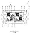
- Fig. 1 shows a power semiconductor module according to the prior art in plan view. Shown is a power semiconductor module (10) consisting of a base plate (20) for Mounting on a heat sink. For this purpose, this base plate (20) in the region of its corners in each case a recess (22).
- the module continues to consist of a frame-like Housing (30) and two electrically insulating substrates (50).
- the respective substrate in turn consists of a Isolierstoff Ari (52) with a plurality of on its first the base plate (20) facing away from the main surface located against each other metallic connecting tracks (54). On its second facing the base plate Main surface has the substrate one of the connecting tracks of the first major surface similar planar metallization on.
- connection elements (42, 44) are here the DC connections, the AC power connection element (40) is duplicated here.
- the connecting tracks (54) of the substrates (50) are partly with each other and with the Connection elements (40) directly or by means of solder bridges (46) connected to each other.
- the Sensor component (58) and to its external contacting according to the prior art For example, one of the substrates has further printed conductors (54a). Both within the Power semiconductor module arranged conductor tracks thus have due to their different functionality on a different design.
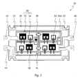
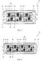
- FIGS. 2 to 4 each show an inventive power semiconductor module (10) in plan view. This differs from the prior art shown in Fig. 1 in that all Substrates (50), regardless of the power-scaling number of Substrates, each designed completely identical. Identical here are the size and Type of Isolierstoff stressess (52) and the arrangement and type of all connecting tracks (54).
- FIG. 2 shows a power semiconductor module (10) with two substrates (50). Both have the same number and configuration of the connecting tracks (54) including the other Connecting tracks (54b) for other functionalities, as here the sensor component (58) on.
- Fig. 3 shows a power semiconductor module (10) compared with 50% higher performance with that of Fig. 2. Both differ only in the length of Power semiconductor module (10) itself and in the number of substrates arranged therein (50). In this case, a substrate further has a sensor component (58) on the other Tracks (54b) on. The other two substrates (50) probably have the tracks (54b), but these are not equipped with components here.
- FIG. 4 shows a power semiconductor module (10) compared with twice the performance with that of Fig. 2. Again, the scaling is done in the same embodiment of outer terminals (40, 42, 44) and the internal connection of the substrates (50) by soldering connector (46) exclusively over a greater length of the module and by the Arrangement of further identical substrates (50).
Landscapes
- Combinations Of Printed Boards (AREA)
- Cooling Or The Like Of Semiconductors Or Solid State Devices (AREA)
Abstract
Description
- Fig. 1
- zeigt ein Leistungshalbleitermodul nach dem Stand der Technik in Draufsicht.
- Fig. 2
- zeigt ein erfindungsgemäßes Leistungshalbleitermodul in Draufsicht.
- Fig. 3
- und 4 zeigen je ein weiteres erfindungsgemäßes Leistungshalbleitermodul unterschiedlicher Leistungsklasse in Draufsicht.
Claims (5)
- Leistungshalbleitermodul (10) in skalierbarer Aufbautechnik mit einer Grundplatte (20) oder zur direkten Montage auf einem Kühlkörper bestehend aus einem rahmenartigen Gehäuse (30), einem Deckel (70), nach außen führenden Anschlusselementen für Last-(40, 42, 44) und Hilfskontakte und mit mindestens zwei innerhalb des Gehäuses (30) angeordneten elektrisch isolierenden Substraten (50), die ihrerseits bestehen aus je einem Isolierstoffkörper (52) und auf dessen der Grundplatte (20) oder dem Kühlkörper abgewandten ersten Hauptfläche befindlichen Mehrzahl von gegeneinander elektrisch isolierten metallischen Verbindungsbahnen (54), darauf befindlichen und mit diesen Verbindungsbahnen schaltungsgerecht verbundenen Leistungshalbleiterbauelementen (56), wobei alle Substrate (50) vollständig identisch ausgestaltet sind, alle Substrate (50) miteinander elektrisch leitend verbunden sind und auf allen Substraten (50) die gleiche Art und Anzahl von Leistungshalbleiterbauelementen (56) angeordnet ist und weiterhin jedes Substrat (50) mindestens eine weitere Leiterbahn (54b) zur Anordnung eines Sensorikbauteils aufweist und auf mindestens einem Substrat ein Sensorikbauteil (58) angeordnet ist.
- Leistungshalbleitermodul (10) nach Anspruch 1, wobei
die Grundplatte (20) eine Mehrzahl von Ausnehmungen (22) zur Schraubverbindung des Leistungshalbleitermoduls mit dem Kühlkörper aufweist. - Leistungshalbleitermodul (10) nach Anspruch 1, wobei
der Isolierstoffkörper (52) des Substrates (50) auf seiner zweiten der Grundplatte (20) oder dem Kühlkörper zugewandten Hauptfläche eine den Verbindungsbahnen (54) der ersten Hauptfläche gleichartige flächige Metallisierung (53) aufweist. - Leistungshalbleitermodul nach Anspruch 4, wobei
eine stoffbündige Verbindung der Grundplatte (20) mit der metallischen Schicht der Substrate (50) aus flächig ausgeführten Lötungen besteht. - Leistungshalbleitermodul (10) nach Anspruch 1, wobei
die gleichartigen Substrate (50) untereinander mittels Lötbrücken (46) verbunden sind.
Applications Claiming Priority (2)
| Application Number | Priority Date | Filing Date | Title |
|---|---|---|---|
| DE10333328 | 2003-07-23 | ||
| DE10333328A DE10333328B3 (de) | 2003-07-23 | 2003-07-23 | Leistungshalbleitermodul in skalierbarer Aufbautechnik |
Publications (2)
| Publication Number | Publication Date |
|---|---|
| EP1501125A2 true EP1501125A2 (de) | 2005-01-26 |
| EP1501125A3 EP1501125A3 (de) | 2006-12-06 |
Family
ID=33483016
Family Applications (1)
| Application Number | Title | Priority Date | Filing Date |
|---|---|---|---|
| EP04014432A Withdrawn EP1501125A3 (de) | 2003-07-23 | 2004-06-19 | Leistungshalbleitermodul mit skalierbarer Aufbautechnik |
Country Status (4)
| Country | Link |
|---|---|
| US (1) | US7164201B2 (de) |
| EP (1) | EP1501125A3 (de) |
| JP (1) | JP2005045237A (de) |
| DE (1) | DE10333328B3 (de) |
Families Citing this family (15)
| Publication number | Priority date | Publication date | Assignee | Title |
|---|---|---|---|---|
| US8279640B2 (en) | 2008-09-24 | 2012-10-02 | Teco-Westinghouse Motor Company | Modular multi-pulse transformer rectifier for use in symmetric multi-level power converter |
| US7830681B2 (en) | 2008-09-24 | 2010-11-09 | Teco-Westinghouse Motor Company | Modular multi-pulse transformer rectifier for use in asymmetric multi-level power converter |
| JP2010129867A (ja) * | 2008-11-28 | 2010-06-10 | Mitsubishi Electric Corp | 電力用半導体装置 |
| US7940537B2 (en) * | 2008-12-31 | 2011-05-10 | Teco-Westinghouse Motor Company | Partial regeneration in a multi-level power inverter |
| US8223515B2 (en) * | 2009-02-26 | 2012-07-17 | TECO—Westinghouse Motor Company | Pre-charging an inverter using an auxiliary winding |
| US8976526B2 (en) | 2009-06-30 | 2015-03-10 | Teco-Westinghouse Motor Company | Providing a cooling system for a medium voltage drive system |
| US8575479B2 (en) | 2009-06-30 | 2013-11-05 | TECO—Westinghouse Motor Company | Providing a transformer for an inverter |
| US8711530B2 (en) * | 2009-06-30 | 2014-04-29 | Teco-Westinghouse Motor Company | Pluggable power cell for an inverter |
| US8130501B2 (en) | 2009-06-30 | 2012-03-06 | Teco-Westinghouse Motor Company | Pluggable power cell for an inverter |
| US8254076B2 (en) | 2009-06-30 | 2012-08-28 | Teco-Westinghouse Motor Company | Providing modular power conversion |
| US8601190B2 (en) | 2011-06-24 | 2013-12-03 | Teco-Westinghouse Motor Company | Providing multiple communication protocols for a control system having a master controller and a slave controller |
| US9363930B2 (en) | 2013-03-11 | 2016-06-07 | Teco-Westinghouse Motor Company | Passive two phase cooling solution for low, medium and high voltage drive systems |
| US9153374B2 (en) | 2013-06-28 | 2015-10-06 | Teco-Westinghouse Motor Company | Cooling arrangements for drive systems |
| US12066780B2 (en) | 2022-05-23 | 2024-08-20 | Ricoh Company, Ltd. | Fixing device including nip formation plate having a plurality of protruding portions and image forming apparatus incorporating same |
| US12490400B2 (en) | 2023-04-11 | 2025-12-02 | Caterpillar Inc. | Flexible power electronics module |
Family Cites Families (9)
| Publication number | Priority date | Publication date | Assignee | Title |
|---|---|---|---|---|
| DE59304797D1 (de) * | 1992-08-26 | 1997-01-30 | Eupec Gmbh & Co Kg | Leistungshalbleiter-Modul |
| JP3269745B2 (ja) * | 1995-01-17 | 2002-04-02 | 株式会社日立製作所 | モジュール型半導体装置 |
| DE19630902B4 (de) * | 1996-08-01 | 2005-07-14 | Ixys Semiconductor Gmbh | Einrichtung zur Temperaturüberwachung in einer leistungselektronischen Anordnung |
| JPH1197598A (ja) * | 1997-09-19 | 1999-04-09 | Toshiba Corp | 半導体装置 |
| DE10024516B4 (de) * | 2000-05-18 | 2006-03-09 | eupec Europäische Gesellschaft für Leistungshalbleiter mbH & Co. KG | Leistungshalbleitermodul |
| JP4089143B2 (ja) * | 2000-08-30 | 2008-05-28 | 三菱電機株式会社 | 電力用半導体装置 |
| WO2002054489A2 (en) * | 2000-12-29 | 2002-07-11 | Advanced Micro Devices, Inc. | Temperature measurement system and method |
| JP4127641B2 (ja) * | 2001-10-23 | 2008-07-30 | 三菱電機株式会社 | 半導体装置 |
| DE10316355C5 (de) * | 2003-04-10 | 2008-03-06 | Semikron Elektronik Gmbh & Co. Kg | Leistungshalbeitermodul mit flexibler äusserer Anschlussbelegung |
-
2003
- 2003-07-23 DE DE10333328A patent/DE10333328B3/de not_active Expired - Fee Related
-
2004
- 2004-06-19 EP EP04014432A patent/EP1501125A3/de not_active Withdrawn
- 2004-07-12 JP JP2004204700A patent/JP2005045237A/ja active Pending
- 2004-07-23 US US10/897,720 patent/US7164201B2/en not_active Expired - Fee Related
Non-Patent Citations (1)
| Title |
|---|
| None * |
Also Published As
| Publication number | Publication date |
|---|---|
| JP2005045237A (ja) | 2005-02-17 |
| EP1501125A3 (de) | 2006-12-06 |
| US7164201B2 (en) | 2007-01-16 |
| DE10333328B3 (de) | 2005-01-27 |
| US20050035439A1 (en) | 2005-02-17 |
Similar Documents
| Publication | Publication Date | Title |
|---|---|---|
| DE10316355B3 (de) | Leistungshalbeitermodul mit flexibler äusserer Anschlussbelegung | |
| DE102004025609B4 (de) | Anordnung in Schraub- Druckkontaktierung mit einem Leistungshalbleitermodul | |
| DE10316356B4 (de) | Modular aufgebautes Leistungshalbleitermodul | |
| EP1592063B1 (de) | Anordnung in Druckkontaktierung mit einem Leistungshalbleitermodul | |
| EP1450404B1 (de) | Anordnung in Druckkontaktierung mit einem Leistungshalbleitermodul | |
| DE10333328B3 (de) | Leistungshalbleitermodul in skalierbarer Aufbautechnik | |
| EP2302782B1 (de) | Stromrichteranordnung | |
| DE102013201931B4 (de) | Laserbauelement und Verfahren zu seiner Herstellung | |
| DE102009011234A1 (de) | Elektronische Baugruppe | |
| DE10141114C1 (de) | Schaltungsanordnung | |
| DE10107839A1 (de) | Anordnung mit einem auf einem Träger montierten integrierten Schaltkreis und einer Stromversorgungsbaugruppenanordnung | |
| DE102005050534B4 (de) | Leistungshalbleitermodul | |
| DE10340297A1 (de) | Schaltungsanordnung für aktive und passive elektrische und elektronische Bauelemente | |
| EP2091081B1 (de) | Schaltungsanordnung mit Bondverbindung | |
| DE102014104013A1 (de) | Leistungshalbleiterbauteil | |
| DE102005030247B4 (de) | Leistungshalbleitermodul mit Verbindungselementen hoher Stromtragfähigkeit | |
| EP1755163B1 (de) | Leistungshalbleitermodul mit Leitungssegment | |
| EP1764832A1 (de) | Bondverbindung für Leistungshalbleiterbauelemente | |
| DE102005039947B4 (de) | Leistungshalbleitermodul mit Befestigungseinrichtung | |
| EP4173039A1 (de) | Leistungshalbleitermodul und herstellungsverfahren für ein leistungshalbleitermodul | |
| WO2005008765A2 (de) | Leistungshalbleitermodul mit vom substrat gelösten leiterbahnenden als externe anschlüsse | |
| DE102024200743A1 (de) | Halbleiterschaltung | |
| DE10256058A1 (de) | Leistungshalbleitermodul mit verbesserten EMV Eigenschaften | |
| DE10249854A1 (de) | Leistungshalbleiter-Baugruppe | |
| DE102021113502A1 (de) | Elektronische Baugruppe mit Platinenverbinder, Elektronikmodul sowie Kraftfahrzeug |
Legal Events
| Date | Code | Title | Description |
|---|---|---|---|
| PUAI | Public reference made under article 153(3) epc to a published international application that has entered the european phase |
Free format text: ORIGINAL CODE: 0009012 |
|
| AK | Designated contracting states |
Kind code of ref document: A2 Designated state(s): AT BE BG CH CY CZ DE DK EE ES FI FR GB GR HU IE IT LI LU MC NL PL PT RO SE SI SK TR |
|
| AX | Request for extension of the european patent |
Extension state: AL HR LT LV MK |
|
| RAP1 | Party data changed (applicant data changed or rights of an application transferred) |
Owner name: SEMIKRON ELEKTRONIK GMBH & CO. KG |
|
| PUAL | Search report despatched |
Free format text: ORIGINAL CODE: 0009013 |
|
| AK | Designated contracting states |
Kind code of ref document: A3 Designated state(s): AT BE BG CH CY CZ DE DK EE ES FI FR GB GR HU IE IT LI LU MC NL PL PT RO SE SI SK TR |
|
| AX | Request for extension of the european patent |
Extension state: AL HR LT LV MK |
|
| RIC1 | Information provided on ipc code assigned before grant |
Ipc: H01L 23/34 20060101ALN20061031BHEP Ipc: H01L 23/52 20060101ALI20061031BHEP Ipc: H01L 23/373 20060101ALI20061031BHEP Ipc: H01L 25/07 20060101AFI20061031BHEP |
|
| 17P | Request for examination filed |
Effective date: 20061108 |
|
| 17Q | First examination report despatched |
Effective date: 20070307 |
|
| AKX | Designation fees paid |
Designated state(s): AT BE BG CH CY CZ DE DK EE ES FI FR GB GR HU IE IT LI LU MC NL PL PT RO SE SI SK TR |
|
| STAA | Information on the status of an ep patent application or granted ep patent |
Free format text: STATUS: THE APPLICATION IS DEEMED TO BE WITHDRAWN |
|
| 18D | Application deemed to be withdrawn |
Effective date: 20150106 |