EP1496537A2 - Connection structure and method of plasma display panel - Google Patents
Connection structure and method of plasma display panel Download PDFInfo
- Publication number
- EP1496537A2 EP1496537A2 EP04254128A EP04254128A EP1496537A2 EP 1496537 A2 EP1496537 A2 EP 1496537A2 EP 04254128 A EP04254128 A EP 04254128A EP 04254128 A EP04254128 A EP 04254128A EP 1496537 A2 EP1496537 A2 EP 1496537A2
- Authority
- EP
- European Patent Office
- Prior art keywords
- panel
- substrate
- electrode
- electrodes
- connection
- Prior art date
- Legal status (The legal status is an assumption and is not a legal conclusion. Google has not performed a legal analysis and makes no representation as to the accuracy of the status listed.)
- Granted
Links
Images






Classifications
-
- H—ELECTRICITY
- H01—ELECTRIC ELEMENTS
- H01J—ELECTRIC DISCHARGE TUBES OR DISCHARGE LAMPS
- H01J11/00—Gas-filled discharge tubes with alternating current induction of the discharge, e.g. alternating current plasma display panels [AC-PDP]; Gas-filled discharge tubes without any main electrode inside the vessel; Gas-filled discharge tubes with at least one main electrode outside the vessel
- H01J11/20—Constructional details
- H01J11/46—Connecting or feeding means, e.g. leading-in conductors
-
- H—ELECTRICITY
- H01—ELECTRIC ELEMENTS
- H01J—ELECTRIC DISCHARGE TUBES OR DISCHARGE LAMPS
- H01J11/00—Gas-filled discharge tubes with alternating current induction of the discharge, e.g. alternating current plasma display panels [AC-PDP]; Gas-filled discharge tubes without any main electrode inside the vessel; Gas-filled discharge tubes with at least one main electrode outside the vessel
- H01J11/10—AC-PDPs with at least one main electrode being out of contact with the plasma
- H01J11/12—AC-PDPs with at least one main electrode being out of contact with the plasma with main electrodes provided on both sides of the discharge space
-
- H—ELECTRICITY
- H01—ELECTRIC ELEMENTS
- H01J—ELECTRIC DISCHARGE TUBES OR DISCHARGE LAMPS
- H01J11/00—Gas-filled discharge tubes with alternating current induction of the discharge, e.g. alternating current plasma display panels [AC-PDP]; Gas-filled discharge tubes without any main electrode inside the vessel; Gas-filled discharge tubes with at least one main electrode outside the vessel
- H01J11/20—Constructional details
- H01J11/22—Electrodes, e.g. special shape, material or configuration
-
- H—ELECTRICITY
- H01—ELECTRIC ELEMENTS
- H01R—ELECTRICALLY-CONDUCTIVE CONNECTIONS; STRUCTURAL ASSOCIATIONS OF A PLURALITY OF MUTUALLY-INSULATED ELECTRICAL CONNECTING ELEMENTS; COUPLING DEVICES; CURRENT COLLECTORS
- H01R12/00—Structural associations of a plurality of mutually-insulated electrical connecting elements, specially adapted for printed circuits, e.g. printed circuit boards [PCB], flat or ribbon cables, or like generally planar structures, e.g. terminal strips, terminal blocks; Coupling devices specially adapted for printed circuits, flat or ribbon cables, or like generally planar structures; Terminals specially adapted for contact with, or insertion into, printed circuits, flat or ribbon cables, or like generally planar structures
- H01R12/50—Fixed connections
- H01R12/51—Fixed connections for rigid printed circuits or like structures
- H01R12/52—Fixed connections for rigid printed circuits or like structures connecting to other rigid printed circuits or like structures
-
- H—ELECTRICITY
- H01—ELECTRIC ELEMENTS
- H01R—ELECTRICALLY-CONDUCTIVE CONNECTIONS; STRUCTURAL ASSOCIATIONS OF A PLURALITY OF MUTUALLY-INSULATED ELECTRICAL CONNECTING ELEMENTS; COUPLING DEVICES; CURRENT COLLECTORS
- H01R12/00—Structural associations of a plurality of mutually-insulated electrical connecting elements, specially adapted for printed circuits, e.g. printed circuit boards [PCB], flat or ribbon cables, or like generally planar structures, e.g. terminal strips, terminal blocks; Coupling devices specially adapted for printed circuits, flat or ribbon cables, or like generally planar structures; Terminals specially adapted for contact with, or insertion into, printed circuits, flat or ribbon cables, or like generally planar structures
- H01R12/70—Coupling devices
- H01R12/7076—Coupling devices for connection between PCB and component, e.g. display
-
- H—ELECTRICITY
- H01—ELECTRIC ELEMENTS
- H01R—ELECTRICALLY-CONDUCTIVE CONNECTIONS; STRUCTURAL ASSOCIATIONS OF A PLURALITY OF MUTUALLY-INSULATED ELECTRICAL CONNECTING ELEMENTS; COUPLING DEVICES; CURRENT COLLECTORS
- H01R13/00—Details of coupling devices of the kinds covered by groups H01R12/70 or H01R24/00 - H01R33/00
- H01R13/02—Contact members
- H01R13/22—Contacts for co-operating by abutting
-
- H—ELECTRICITY
- H01—ELECTRIC ELEMENTS
- H01R—ELECTRICALLY-CONDUCTIVE CONNECTIONS; STRUCTURAL ASSOCIATIONS OF A PLURALITY OF MUTUALLY-INSULATED ELECTRICAL CONNECTING ELEMENTS; COUPLING DEVICES; CURRENT COLLECTORS
- H01R4/00—Electrically-conductive connections between two or more conductive members in direct contact, i.e. touching one another; Means for effecting or maintaining such contact; Electrically-conductive connections having two or more spaced connecting locations for conductors and using contact members penetrating insulation
- H01R4/26—Connections in which at least one of the connecting parts has projections which bite into or engage the other connecting part in order to improve the contact
-
- H—ELECTRICITY
- H05—ELECTRIC TECHNIQUES NOT OTHERWISE PROVIDED FOR
- H05K—PRINTED CIRCUITS; CASINGS OR CONSTRUCTIONAL DETAILS OF ELECTRIC APPARATUS; MANUFACTURE OF ASSEMBLAGES OF ELECTRICAL COMPONENTS
- H05K3/00—Apparatus or processes for manufacturing printed circuits
- H05K3/36—Assembling printed circuits with other printed circuits
- H05K3/361—Assembling flexible printed circuits with other printed circuits
-
- H—ELECTRICITY
- H05—ELECTRIC TECHNIQUES NOT OTHERWISE PROVIDED FOR
- H05K—PRINTED CIRCUITS; CASINGS OR CONSTRUCTIONAL DETAILS OF ELECTRIC APPARATUS; MANUFACTURE OF ASSEMBLAGES OF ELECTRICAL COMPONENTS
- H05K2201/00—Indexing scheme relating to printed circuits covered by H05K1/00
- H05K2201/03—Conductive materials
- H05K2201/0332—Structure of the conductor
- H05K2201/0364—Conductor shape
- H05K2201/0367—Metallic bump or raised conductor not used as solder bump
-
- H—ELECTRICITY
- H05—ELECTRIC TECHNIQUES NOT OTHERWISE PROVIDED FOR
- H05K—PRINTED CIRCUITS; CASINGS OR CONSTRUCTIONAL DETAILS OF ELECTRIC APPARATUS; MANUFACTURE OF ASSEMBLAGES OF ELECTRICAL COMPONENTS
- H05K3/00—Apparatus or processes for manufacturing printed circuits
- H05K3/30—Assembling printed circuits with electric components, e.g. with resistors
- H05K3/32—Assembling printed circuits with electric components, e.g. with resistors electrically connecting electric components or wires to printed circuits
- H05K3/321—Assembling printed circuits with electric components, e.g. with resistors electrically connecting electric components or wires to printed circuits by conductive adhesives
- H05K3/323—Assembling printed circuits with electric components, e.g. with resistors electrically connecting electric components or wires to printed circuits by conductive adhesives by applying an anisotropic conductive adhesive layer over an array of pads
-
- H—ELECTRICITY
- H10—SEMICONDUCTOR DEVICES; ELECTRIC SOLID-STATE DEVICES NOT OTHERWISE PROVIDED FOR
- H10W—GENERIC PACKAGES, INTERCONNECTIONS, CONNECTORS OR OTHER CONSTRUCTIONAL DETAILS OF DEVICES COVERED BY CLASS H10
- H10W74/00—Encapsulations, e.g. protective coatings
- H10W74/10—Encapsulations, e.g. protective coatings characterised by their shape or disposition
- H10W74/15—Encapsulations, e.g. protective coatings characterised by their shape or disposition on active surfaces of flip-chip devices, e.g. underfills
Definitions
- the present invention relates to a plasma display panel, and in particular but not exclusively to a connection structure and method of a plasma display panel that electrically connects a panel substrate with a connection member such as anisotropic conductive film or a printed circuit board PCB with the connection member.
- a connection member such as anisotropic conductive film or a printed circuit board PCB with the connection member.
- Display means are becoming more important, as the principal man-machine interface for displaying such image information.
- the display means can be applied to LCD, TV or AV monitor and computer display.
- Plasma Display Panel (hereinafter "PDP") among the display means has an advantage of being thin and light and being able to be made into a large size.
- the PDP may include a panel to generate electric discharge, a printed circuit board having a drive circuit to control the panel and other devices such as heatproof device.
- Anisotropic Conductive Film (ACF) is used to electrically connect the panel and the printed circuit board.
- a plurality of flexible substrates 2 for signal connection are stuck to a panel substrate 1 of rectangular shape.
- An anisotropic conductive film (ACF) 3 is stuck to the end of the flexible substrate 2 in order to adhere the panel substrate 1 to the flexible substrate 2, thus the end of the panel substrate 1 and the end of the flexible substrate 2 are stuck to each other and, at the same time, electrically connected to each other.
- the anisotropic conductive film 3 currently used has a double layer structure of epoxy resin 5 including conductive balls 4 as shown in FIG. 3.
- the reference numeral '6' represents PET resin to protect the anisotropic conductive film 3.
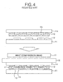
- FIG. 4 is a diagram representing a panel substrate that is connected to a flexible substrate by use of an anisotropic conductive film of prior art.
- a flexible substrate 14 e.g., Chip On FilmCOF, Flexible Printed Circuit Film FPC
- a silicon rubber 16 is put on the flexible substrate 14 mounted in this way, and then pressure is applied to the flexible substrate 14 by use of a heat compression head 17 of a compressor (not shown).
- the silicon rubber 16 is a buffer to prevent the panel substrate 11 frombeing damaged by the pressure applied by the compressor.
- a copper CU electrode 15 and an address electrode 12 of the panel substrate 11 are located having conductive balls 4 therebetween, wherein the conductive balls 4 exist in the anisotropic conductive film 13.
- the epoxy resin of the anisotropic conductive film 13 fills a space area where the copper electrode 15 and the address electrode 12 are not located, i.e., which is formed between the copper electrodes 15 and between the address electrodes 12.
- the panel substrate 11 and the flexible substrate 14 are electrically connected by the conductive balls 4, and they are insulated by the epoxy resin between the copper electrodes 15 and between the address electrodes 12.
- connection structure of prior art that the panel substrate is electrically connected with the flexible substrate by use of the conductive balls, it is possible to be electrically connected by the conductive balls, but such conductive balls cause the cohesiveness of the electrode of the panel substrate and the electrode of the flexible substrate to be weak, so there is high degree of possibility that the connection part breaks away.
- connection structure and associated method for plasma display panels to make electrical connections without using conductive balls.
- connection structure and associated method forplasma displaypanels so as to increase connection cohesiveness by having the electrode of a flexible substrate protruding to penetrate the electrode of a panel substrate.
- a connection structure for a plasma display panel includes a first substrate having a plurality of panel-electrodes; a second substrate having a plurality of connecting- electrodes arranged to correspond to the panel-electrodes; and a connection member located between the first substrate and the secondsubstratetodirectlyconnecttheconnecting-electrodes with the panel-electrodes upon compression.
- the connecting-electrode has a projected shape with an angle in the connection member direction.
- the connecting-electrode has a projected shape with a curved surface in the connection member direction.
- the connecting-electrode penetrates into the inside of the panel-electrode upon compression.
- the second substrate is an anisotropic conductive film FPC, a chip-on-film COF or a chip-on-glass COG.
- the panel-electrode may be an address electrode if the first substrate is a lower substrate.
- the panel-electrode may be a bus electrode if the first substrate is an upper substrate.
- connection member may be made of any one among an epoxy resin with no conductive ball therein, a styrene resin with no conductive ball therein, an urethane resin with no conductive ball therein, a phenol resin with no conductive ball therein or a silicon resin with no conductive ball therein.
- a connection method for a plasma display panel includes the steps of: mounting a second substrate on a first substrate, wherein the first substrate includes a plurality of panel-electrodes and the second substrate includes a plurality of connecting-electrodes and a connection member made of a resin material with no conductive ball therein; aligning the connecting-electrodes with the panel-electrodes to correspond to each other; and directly connecting the connecting-electrodes with the panel-electrodes by having pressure applied to the second substrate for the connecting-electrodes to penetrate the epoxy resin.
- the connecting-electrode has a projected shape with an angle in the connection member direction.
- the connecting-electrode has a projected shape with a curved surface in the connection member direction.
- the connecting-electrode penetrates into the inside of the panel-electrode.
- the second substrate is an anisotropic conductive Film FPC, a chip-on-film COF or a chip-on-glass COG.
- the panel-electrode may be one of an address electrode or a bus electrode.
- the resin material may be one among an epoxy resin, a styrene resin, an urethane resin, a phenol resin and a silicon resin.
- the invention also provides a plasma display panel comprising the connection structure set out above, and a method of constructing a plasma display panel comprising the method steps set out above.
- FIG. 6 is a diagram representing the connection structure of a plasma display panel according to a desirable embodiment of the present invention.
- connection structure of a plasma display panel is desirable to include a panel substrate 53, a flexible substrate 51 and a connection member 55.
- the panel substrate 53 includes a plurality of panel-electrodes 54.
- the flexible substrate 51 includes a plurality of connection-electrodes, e.g., copper electrodes 52, arranged to correspond to the panel-electrodes 54.
- the connection member 55 is located between the panel substrate 53 and the flexible substrate 51 and, upon compression, guides the connection-electrode to be connected direct with the panel-electrode 54 (address electrode or bus electrode).
- connection member 55 is desirable to be made of any one of the epoxy resin with no conductive ball therein, the styrene resin with no conductive ball therein, the urethane resin with no conductive ball therein, the phenol resin with no conductive ball therein or the silicon resin with no conductive ball therein.
- connection member 55 is described as an anisotropic conductive film ACF, however the connection member of the present invention is not only limited to the anisotropic conductive member but it may also include an isotropic conductive film.
- the panel substrate 53 might be a lower substrate or an upper substrate of a plasma display panel.
- the panel-electrode 54 is an address electrode.
- the panel-electrode 54 is a bus electrode.
- the flexible substrate 51 might be one of Flexible Printed Circuit Film FPC, Chip On Film COF or Chip On Glass COG.
- a copper electrode 52 formed in the flexible substrate 51 might have a projected shape with an angle in the anisotropic conductive film 55 direction. That is, as shown in FIG. 8, the copper electrode 61 might have a plurality of triangular shapes within the width of the panel-electrode 62. At this moment, the triangular shapes can be uniform, or the triangular shapes in the middle can be formed to be bigger than the triangular shapes in the edge.
- the copper electrode 61 of the projected shape with such an angle penetrates the panel-electrode 62 corresponding thereto upon compression to increase the connection cohesiveness of the panel-electrode 62 and the copper electrode 61, thereby preventing the panel substrate frombeing separated from the flexible substrate due to weak cohesiveness of the prior art.
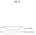
- the copper electrode 52 might have a projected shape with a curved surface in the anisotropic conductive film 55 direction. That is, as shown in FIG. 9, the copper electrode 64 might be formed to be projected in a smooth curved surface (semi-oval or semicircle) that it is biggest in its middle part and gets smaller gradually.
- the copper electrode 64 has a projected shape with a curved surface, thus its contact surface is maximized with the panel-electrode 62 upon compression to restrain the electrical resistance component in the connection part to the highest degree, thereby improving its conductive capacity.
- the edge of the panel electrode 66 is formed in an edge-curl shape. That is, the edge of the penal electrode 66 is formed to be high and, as it gets to the middle, it is formed to low. (refer to FIG. 10)
- the copper electrode 67 is formed to have a projected shape with an angle at each of a middle part 68 and both edge parts 69 but the projected shape of the middle part 68 is made to be bigger than the projected shape of both edge parts 69.
- the projected shape formed at the middle part 68 and both edge parts 69 uniformly penetrates the panel-electrode 66, thereby improving the connection cohesiveness more.
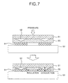
- FIG. 7 is a diagram representing a panel substrate connected with a flexible substrate by use of an anisotropic conductive film according to a desirable embodiment of the present invention.
- a panel substrate 53 including a plurality of panel-electrodes 54, an anisotropic conductive film 55 made of epoxy resin with no conductive ball therein, and a flexible substrate 51 including a plurality of copper electrodes 52.
- the anisotropic conductive film 55 and the flexible substrate 51 are mounted in turn on the panel substrate 53 provided in this way.
- the flexible substrate 51 is pressed by the compression head of the heat compression device, and accordingly, the copper electrode 52 of the flexible substrate 51 penetrates the epoxy resin of the anisotropic conductive film 55 and is directly connected to the panel-electrode 54 of the panel substrate 53.
- the panel-electrode is indirectly connected to the copper electrode by the conductive balls in the prior art, in the present invention, because there is no conductive ball in the anisotropic conductive film 55, the copper electrode 52 of the flexible substrate 51 penetrates the epoxy resin and is directly connected to the panel-electrode 54 of the panel substrate 53.
- the copper electrode 52 connected to the panel-electrode 54 in this way gradually penetrates the panel-electrode 54 at a designated depth as pressure increases and time passes by. At this moment, it is not within the scope of the present invention how deep the copper electrode 52 penetrates, thus it will not described further, but only if the copper electrode 52 penetrates the panel-electrode 54 at a designated depth in this invention, there will be no obstacle in realizing this invention.
- connection structure of the plasma display panel but the present invention is not limited to this, but attention should be given to the fact that it can be applicable to all display devices such as LCD and EL etc that require to be electrically connected by use of the flexible substrate including the copper electrode having a projected shape with an angle and the anisotropic conductive film with no conductive ball therein.
- connection structure and method of the plasma display panel use the connection member with no conductive ball therein, thereby preventing the occurrence of short circuit caused by the conductive ball mass of prior art. Also, the conductive ball like this is not used, so that it is expected to have an effect of saving material cost more than before.
- connection structure and method of the plasma display panel have the copper electrode of the flexible substrate formed in a projected shape with an angle, so the copper electrode penetrates the panel-electrode of the panel substrate, thereby improving the connection cohesiveness between the flexible substrate and the panel substrate.
Landscapes
- Engineering & Computer Science (AREA)
- Physics & Mathematics (AREA)
- Plasma & Fusion (AREA)
- Manufacturing & Machinery (AREA)
- Microelectronics & Electronic Packaging (AREA)
- Chemical & Material Sciences (AREA)
- Materials Engineering (AREA)
- Devices For Indicating Variable Information By Combining Individual Elements (AREA)
- Gas-Filled Discharge Tubes (AREA)
Abstract
Description
Claims (17)
- A connection structure of a plasma display panel, comprising:a first substrate having a plurality of panel-electrodes;a second substrate having a plurality of connecting-electrodes arranged to correspond to the panel-electrodes; anda connection member located between the first substrate and the second substrate to directly connect the connecting-electrodes with the panel-electrodes upon compression.
- The connection structure according to claim 1, wherein the connecting-electrode has a projected shape with an angle in the connection member direction.
- The connection structure according to claim 1, wherein the connecting-electrode has a projected shape with a curved surface in the connection member direction.
- The connection structure according to claim 1, wherein the connecting-electrode penetrates into the inside of the panel-electrode upon compression.
- The connection structure according to claim 1, wherein the second substrate is an anisotropic conductive film FPC, a chip-on-film COF or a chip-on-glass COG.
- The connection structure according to claim 1, wherein the panel-electrode is an address electrode if the first substrate is a lower substrate.
- The connection structure according to claim 1, wherein the panel-electrode is a bus electrode if the first substrate is an upper substrate.
- The connection structure according to claim 1, wherein the connection member is made of any one among an epoxy resin with no conductive ball therein, a styrene resin with no conductive ball therein, an urethane resin with no conductive ball therein, a phenol resin with no conductive ball therein and a silicon resin with no conductive ball therein.
- A connection method of a plasma display panel, comprising the steps of:mounting a second substrate on a first substrate, wherein the first substrate includes a plurality of panel-electrodes and the second substrate includes a plurality of connecting-electrodes and a connection member made of a resin material with no conductive ball therein;aligning the connecting-electrodes with the panel-electrodes to correspond to each other; anddirectly connecting the connecting-electrodes with the panel-electrodes by having pressure applied to the second substrate for the connecting-electrodes to penetrate the epoxy resin.
- The connection method according to claim 9, wherein the connecting-electrode has a projected shape with an angle in the connection member direction.
- The connection method according to claim 9, wherein the connecting-electrode has a projected shape with a curved surface in the connection member direction.
- The connection method according to claim 9, wherein the connecting-electrode penetrates into the inside of the panel-electrode.
- The connection method according to claim 9, wherein the second substrate is an anisotropic conductive film FPC, a chip-on-film COF and a chip-on-glass COG.
- The connection method according to claim 9, wherein the panel-electrode is one of an address electrode or a bus electrode.
- The connection method according to claim 9, wherein the resin material is one among an epoxy resin, a styrene resin, an urethane resin, a phenol resin and a silicon resin.
- A plasma display panel comprising the connection structure of any of claims 1 to 8.
- A method of fabricating a plasma display panel comprising the steps of any of claims 9 to 15.
Applications Claiming Priority (2)
| Application Number | Priority Date | Filing Date | Title |
|---|---|---|---|
| KR2003046330 | 2003-07-09 | ||
| KR10-2003-0046330A KR100512992B1 (en) | 2003-07-09 | 2003-07-09 | Connection structure of plasma display panel and structure method thereof |
Publications (3)
| Publication Number | Publication Date |
|---|---|
| EP1496537A2 true EP1496537A2 (en) | 2005-01-12 |
| EP1496537A3 EP1496537A3 (en) | 2007-07-25 |
| EP1496537B1 EP1496537B1 (en) | 2013-01-09 |
Family
ID=33448367
Family Applications (1)
| Application Number | Title | Priority Date | Filing Date |
|---|---|---|---|
| EP04254128A Expired - Lifetime EP1496537B1 (en) | 2003-07-09 | 2004-07-09 | Connection structure and method of plasma display panel |
Country Status (5)
| Country | Link |
|---|---|
| US (1) | US7211951B2 (en) |
| EP (1) | EP1496537B1 (en) |
| JP (1) | JP2005031684A (en) |
| KR (1) | KR100512992B1 (en) |
| CN (1) | CN100350542C (en) |
Cited By (2)
| Publication number | Priority date | Publication date | Assignee | Title |
|---|---|---|---|---|
| EP1693876A3 (en) * | 2005-02-17 | 2009-04-01 | LG Electronics Inc. | Plasma display apparatus comprising connector |
| EP3035117A1 (en) * | 2014-12-16 | 2016-06-22 | Gemalto Sa | Method for manufacturing a display device |
Families Citing this family (9)
| Publication number | Priority date | Publication date | Assignee | Title |
|---|---|---|---|---|
| KR100715877B1 (en) * | 2005-09-14 | 2007-05-08 | (주)아이디에스 | Flexible circuit board with an outer layer of laminated coverlay film |
| JP5128773B2 (en) * | 2006-01-23 | 2013-01-23 | 日本電気株式会社 | Manufacturing method of liquid crystal display device |
| KR100777732B1 (en) * | 2006-03-02 | 2007-11-19 | 삼성에스디아이 주식회사 | Plasma display panel |
| KR20090057719A (en) * | 2007-12-03 | 2009-06-08 | 엘지전자 주식회사 | Plasma display device |
| TW201123377A (en) * | 2009-12-16 | 2011-07-01 | Raydium Semiconductor Corp | Electronic chip and substrate with void |
| US10172241B2 (en) * | 2013-09-13 | 2019-01-01 | Korea Advanced Institute Of Science And Technology | Method for packaging flexible device using holding wafer, and flexible device manufactured by the same |
| CN104754866B (en) * | 2013-12-27 | 2019-01-04 | 昆山国显光电有限公司 | Flexible printed circuit board and its manufacturing method and flat-panel monitor |
| KR102662413B1 (en) * | 2017-12-29 | 2024-04-30 | 엘지디스플레이 주식회사 | Electrode connection structure for display panel |
| KR20200145877A (en) * | 2019-06-19 | 2020-12-31 | 삼성디스플레이 주식회사 | Display device, manufacturing apparatus of chip on film ,and manufacturing method of chip on film |
Family Cites Families (16)
| Publication number | Priority date | Publication date | Assignee | Title |
|---|---|---|---|---|
| JPS5085297A (en) * | 1973-11-29 | 1975-07-09 | ||
| JP2827650B2 (en) * | 1992-01-14 | 1998-11-25 | 松下電器産業株式会社 | Thermocompression bonding method and crimping member |
| US5785535A (en) * | 1996-01-17 | 1998-07-28 | International Business Machines Corporation | Computer system with surface mount socket |
| JP2896458B2 (en) * | 1996-09-02 | 1999-05-31 | 株式会社日立製作所 | Flat panel display |
| JP2006276881A (en) * | 1997-04-30 | 2006-10-12 | Matsushita Electric Ind Co Ltd | Method for manufacturing plasma display panel |
| US6086441A (en) * | 1997-04-30 | 2000-07-11 | Matsushita Electric Industrial Co., Ltd. | Method for connecting electrodes of plasma display panel |
| JP3492195B2 (en) * | 1997-04-30 | 2004-02-03 | 松下電器産業株式会社 | Electrode bonding method for plasma display panel |
| JPH1140064A (en) * | 1997-07-25 | 1999-02-12 | Hitachi Ltd | Gas discharge type display panel and display device using the same |
| JP3561137B2 (en) * | 1998-01-19 | 2004-09-02 | 株式会社エンプラス | Display panel inspection socket |
| JP3705914B2 (en) * | 1998-01-27 | 2005-10-12 | 三菱電機株式会社 | Surface discharge type plasma display panel and manufacturing method thereof |
| JPH11273577A (en) * | 1998-03-20 | 1999-10-08 | Dainippon Printing Co Ltd | Electrode terminal of plasma display panel |
| JP3462135B2 (en) * | 1999-01-14 | 2003-11-05 | シャープ株式会社 | Two-dimensional image detector, active matrix substrate, and display device |
| JP3259771B2 (en) * | 1999-01-25 | 2002-02-25 | 日本電気株式会社 | Plasma display panel |
| JP2001305570A (en) * | 2000-04-24 | 2001-10-31 | Nec Corp | Display panel module and its manufacturing method |
| JP4107787B2 (en) | 2000-06-09 | 2008-06-25 | パイオニア株式会社 | Plasma display panel and manufacturing method thereof |
| JP2002108231A (en) * | 2000-09-27 | 2002-04-10 | Fujitsu Ltd | Connection member and matrix-type display device |
-
2003
- 2003-07-09 KR KR10-2003-0046330A patent/KR100512992B1/en not_active Expired - Fee Related
-
2004
- 2004-07-08 US US10/885,695 patent/US7211951B2/en not_active Expired - Fee Related
- 2004-07-09 EP EP04254128A patent/EP1496537B1/en not_active Expired - Lifetime
- 2004-07-09 JP JP2004203508A patent/JP2005031684A/en active Pending
- 2004-07-09 CN CNB2004100900054A patent/CN100350542C/en not_active Expired - Fee Related
Cited By (6)
| Publication number | Priority date | Publication date | Assignee | Title |
|---|---|---|---|---|
| EP1693876A3 (en) * | 2005-02-17 | 2009-04-01 | LG Electronics Inc. | Plasma display apparatus comprising connector |
| US7612501B2 (en) | 2005-02-17 | 2009-11-03 | Lg Electronics Inc. | Plasma display apparatus comprising connector |
| CN1822285B (en) * | 2005-02-17 | 2010-05-26 | Lg电子株式会社 | Plasma display apparatus comprising connector |
| US7821204B2 (en) | 2005-02-17 | 2010-10-26 | Lg Electronics Inc. | Plasma display apparatus comprising connector |
| US8011989B2 (en) | 2005-02-17 | 2011-09-06 | Lg Electronics Inc. | Method of making a plasma display panel with a novel connection structure |
| EP3035117A1 (en) * | 2014-12-16 | 2016-06-22 | Gemalto Sa | Method for manufacturing a display device |
Also Published As
| Publication number | Publication date |
|---|---|
| US7211951B2 (en) | 2007-05-01 |
| KR20050006496A (en) | 2005-01-17 |
| CN1599005A (en) | 2005-03-23 |
| KR100512992B1 (en) | 2005-09-05 |
| US20050006650A1 (en) | 2005-01-13 |
| JP2005031684A (en) | 2005-02-03 |
| CN100350542C (en) | 2007-11-21 |
| EP1496537B1 (en) | 2013-01-09 |
| EP1496537A3 (en) | 2007-07-25 |
Similar Documents
| Publication | Publication Date | Title |
|---|---|---|
| US7164460B2 (en) | Mounting structure for semiconductor device, electro-optical device, and electronic apparatus | |
| US6819370B2 (en) | Liquid crystal display panel including two PGB for outputting signals to the same conductive wires and a repair line | |
| US20100141617A1 (en) | Display driver integrated circuit device, film, and module | |
| KR100637429B1 (en) | Plasma display device | |
| EP1496537B1 (en) | Connection structure and method of plasma display panel | |
| JP2005203745A (en) | Driving chip and display device having the same | |
| EP0501413A2 (en) | Plane-type display apparatus | |
| CN1171117C (en) | Electro-optical device, method of manufacturing electro-optical device, and electronic apparatus | |
| EP1780588A1 (en) | Liquid crystal display device | |
| CN101726874B (en) | Connecting structure for display panel and flexible circuit board | |
| JP2002063958A (en) | Electro-optical devices and electronic equipment | |
| JPH0836189A (en) | LCD display module | |
| US9477123B2 (en) | Liquid crystal display device and production method thereof | |
| CN100480786C (en) | Composite crystal structure of glass, and LCD of using the composite crystal structure of glass | |
| WO2020107654A1 (en) | Display screen and display apparatus | |
| US20080061696A1 (en) | Plasma display apparatus comprising connector | |
| CN101206369A (en) | Pixel array module and flat display device | |
| KR100762700B1 (en) | Flat panel display with tape carrier package | |
| KR100578961B1 (en) | Plasma Display Device With Tape Carrier Package | |
| CN109031733B (en) | Flexible circuit board and display device | |
| EP3786698B1 (en) | Auxiliary coupling layer and display device having the same | |
| KR100966426B1 (en) | Bonding structure of tape carrier package and pad of LCD | |
| JP2003280027A (en) | Liquid crystal display | |
| KR100457550B1 (en) | Drive module re-application method | |
| KR100886238B1 (en) | Flat Panel Display |
Legal Events
| Date | Code | Title | Description |
|---|---|---|---|
| PUAI | Public reference made under article 153(3) epc to a published international application that has entered the european phase |
Free format text: ORIGINAL CODE: 0009012 |
|
| AK | Designated contracting states |
Kind code of ref document: A2 Designated state(s): AT BE BG CH CY CZ DE DK EE ES FI FR GB GR HU IE IT LI LU MC NL PL PT RO SE SI SK TR |
|
| AX | Request for extension of the european patent |
Extension state: AL HR LT LV MK |
|
| RIN1 | Information on inventor provided before grant (corrected) |
Inventor name: PARK, SEUNG TEA,NO. 106-1402 DONGYANG HANSIN Inventor name: KIM, SOON HAK Inventor name: CHOI, YONG GI |
|
| PUAL | Search report despatched |
Free format text: ORIGINAL CODE: 0009013 |
|
| AK | Designated contracting states |
Kind code of ref document: A3 Designated state(s): AT BE BG CH CY CZ DE DK EE ES FI FR GB GR HU IE IT LI LU MC NL PL PT RO SE SI SK TR |
|
| AX | Request for extension of the european patent |
Extension state: AL HR LT LV MK |
|
| 17P | Request for examination filed |
Effective date: 20080116 |
|
| 17Q | First examination report despatched |
Effective date: 20080219 |
|
| AKX | Designation fees paid |
Designated state(s): DE FR GB NL |
|
| REG | Reference to a national code |
Ref country code: DE Ref legal event code: R079 Ref document number: 602004040706 Country of ref document: DE Free format text: PREVIOUS MAIN CLASS: H01J0017180000 Ipc: H01J0011460000 |
|
| GRAP | Despatch of communication of intention to grant a patent |
Free format text: ORIGINAL CODE: EPIDOSNIGR1 |
|
| RIC1 | Information provided on ipc code assigned before grant |
Ipc: H01J 11/46 20120101AFI20120709BHEP |
|
| GRAS | Grant fee paid |
Free format text: ORIGINAL CODE: EPIDOSNIGR3 |
|
| GRAA | (expected) grant |
Free format text: ORIGINAL CODE: 0009210 |
|
| AK | Designated contracting states |
Kind code of ref document: B1 Designated state(s): DE FR GB NL |
|
| REG | Reference to a national code |
Ref country code: GB Ref legal event code: FG4D |
|
| REG | Reference to a national code |
Ref country code: DE Ref legal event code: R096 Ref document number: 602004040706 Country of ref document: DE Effective date: 20130307 |
|
| REG | Reference to a national code |
Ref country code: NL Ref legal event code: T3 |
|
| PGFP | Annual fee paid to national office [announced via postgrant information from national office to epo] |
Ref country code: NL Payment date: 20130612 Year of fee payment: 10 |
|
| PGFP | Annual fee paid to national office [announced via postgrant information from national office to epo] |
Ref country code: DE Payment date: 20130611 Year of fee payment: 10 |
|
| PLBE | No opposition filed within time limit |
Free format text: ORIGINAL CODE: 0009261 |
|
| STAA | Information on the status of an ep patent application or granted ep patent |
Free format text: STATUS: NO OPPOSITION FILED WITHIN TIME LIMIT |
|
| 26N | No opposition filed |
Effective date: 20131010 |
|
| REG | Reference to a national code |
Ref country code: DE Ref legal event code: R097 Ref document number: 602004040706 Country of ref document: DE Effective date: 20131010 |
|
| GBPC | Gb: european patent ceased through non-payment of renewal fee |
Effective date: 20130709 |
|
| REG | Reference to a national code |
Ref country code: FR Ref legal event code: ST Effective date: 20140331 |
|
| PG25 | Lapsed in a contracting state [announced via postgrant information from national office to epo] |
Ref country code: GB Free format text: LAPSE BECAUSE OF NON-PAYMENT OF DUE FEES Effective date: 20130709 |
|
| PG25 | Lapsed in a contracting state [announced via postgrant information from national office to epo] |
Ref country code: FR Free format text: LAPSE BECAUSE OF NON-PAYMENT OF DUE FEES Effective date: 20130731 |
|
| REG | Reference to a national code |
Ref country code: DE Ref legal event code: R119 Ref document number: 602004040706 Country of ref document: DE |
|
| REG | Reference to a national code |
Ref country code: NL Ref legal event code: V1 Effective date: 20150201 |
|
| PG25 | Lapsed in a contracting state [announced via postgrant information from national office to epo] |
Ref country code: NL Free format text: LAPSE BECAUSE OF NON-PAYMENT OF DUE FEES Effective date: 20150201 |
|
| PG25 | Lapsed in a contracting state [announced via postgrant information from national office to epo] |
Ref country code: DE Free format text: LAPSE BECAUSE OF NON-PAYMENT OF DUE FEES Effective date: 20150203 |
|
| REG | Reference to a national code |
Ref country code: DE Ref legal event code: R119 Ref document number: 602004040706 Country of ref document: DE Effective date: 20150203 |