CN100350542C - Connection structure and method of plasma display panel - Google Patents
Connection structure and method of plasma display panel Download PDFInfo
- Publication number
- CN100350542C CN100350542C CNB2004100900054A CN200410090005A CN100350542C CN 100350542 C CN100350542 C CN 100350542C CN B2004100900054 A CNB2004100900054 A CN B2004100900054A CN 200410090005 A CN200410090005 A CN 200410090005A CN 100350542 C CN100350542 C CN 100350542C
- Authority
- CN
- China
- Prior art keywords
- electrode
- substrate
- panel
- syndeton
- connection electrode
- Prior art date
- Legal status (The legal status is an assumption and is not a legal conclusion. Google has not performed a legal analysis and makes no representation as to the accuracy of the status listed.)
- Expired - Fee Related
Links
Images


Classifications
-
- H—ELECTRICITY
- H01—ELECTRIC ELEMENTS
- H01J—ELECTRIC DISCHARGE TUBES OR DISCHARGE LAMPS
- H01J11/00—Gas-filled discharge tubes with alternating current induction of the discharge, e.g. alternating current plasma display panels [AC-PDP]; Gas-filled discharge tubes without any main electrode inside the vessel; Gas-filled discharge tubes with at least one main electrode outside the vessel
- H01J11/20—Constructional details
- H01J11/46—Connecting or feeding means, e.g. leading-in conductors
-
- H—ELECTRICITY
- H01—ELECTRIC ELEMENTS
- H01J—ELECTRIC DISCHARGE TUBES OR DISCHARGE LAMPS
- H01J11/00—Gas-filled discharge tubes with alternating current induction of the discharge, e.g. alternating current plasma display panels [AC-PDP]; Gas-filled discharge tubes without any main electrode inside the vessel; Gas-filled discharge tubes with at least one main electrode outside the vessel
- H01J11/10—AC-PDPs with at least one main electrode being out of contact with the plasma
- H01J11/12—AC-PDPs with at least one main electrode being out of contact with the plasma with main electrodes provided on both sides of the discharge space
-
- H—ELECTRICITY
- H01—ELECTRIC ELEMENTS
- H01J—ELECTRIC DISCHARGE TUBES OR DISCHARGE LAMPS
- H01J11/00—Gas-filled discharge tubes with alternating current induction of the discharge, e.g. alternating current plasma display panels [AC-PDP]; Gas-filled discharge tubes without any main electrode inside the vessel; Gas-filled discharge tubes with at least one main electrode outside the vessel
- H01J11/20—Constructional details
- H01J11/22—Electrodes, e.g. special shape, material or configuration
-
- H—ELECTRICITY
- H01—ELECTRIC ELEMENTS
- H01R—ELECTRICALLY-CONDUCTIVE CONNECTIONS; STRUCTURAL ASSOCIATIONS OF A PLURALITY OF MUTUALLY-INSULATED ELECTRICAL CONNECTING ELEMENTS; COUPLING DEVICES; CURRENT COLLECTORS
- H01R12/00—Structural associations of a plurality of mutually-insulated electrical connecting elements, specially adapted for printed circuits, e.g. printed circuit boards [PCB], flat or ribbon cables, or like generally planar structures, e.g. terminal strips, terminal blocks; Coupling devices specially adapted for printed circuits, flat or ribbon cables, or like generally planar structures; Terminals specially adapted for contact with, or insertion into, printed circuits, flat or ribbon cables, or like generally planar structures
- H01R12/50—Fixed connections
- H01R12/51—Fixed connections for rigid printed circuits or like structures
- H01R12/52—Fixed connections for rigid printed circuits or like structures connecting to other rigid printed circuits or like structures
-
- H—ELECTRICITY
- H01—ELECTRIC ELEMENTS
- H01R—ELECTRICALLY-CONDUCTIVE CONNECTIONS; STRUCTURAL ASSOCIATIONS OF A PLURALITY OF MUTUALLY-INSULATED ELECTRICAL CONNECTING ELEMENTS; COUPLING DEVICES; CURRENT COLLECTORS
- H01R12/00—Structural associations of a plurality of mutually-insulated electrical connecting elements, specially adapted for printed circuits, e.g. printed circuit boards [PCB], flat or ribbon cables, or like generally planar structures, e.g. terminal strips, terminal blocks; Coupling devices specially adapted for printed circuits, flat or ribbon cables, or like generally planar structures; Terminals specially adapted for contact with, or insertion into, printed circuits, flat or ribbon cables, or like generally planar structures
- H01R12/70—Coupling devices
- H01R12/7076—Coupling devices for connection between PCB and component, e.g. display
-
- H—ELECTRICITY
- H01—ELECTRIC ELEMENTS
- H01R—ELECTRICALLY-CONDUCTIVE CONNECTIONS; STRUCTURAL ASSOCIATIONS OF A PLURALITY OF MUTUALLY-INSULATED ELECTRICAL CONNECTING ELEMENTS; COUPLING DEVICES; CURRENT COLLECTORS
- H01R13/00—Details of coupling devices of the kinds covered by groups H01R12/70 or H01R24/00 - H01R33/00
- H01R13/02—Contact members
- H01R13/22—Contacts for co-operating by abutting
-
- H—ELECTRICITY
- H01—ELECTRIC ELEMENTS
- H01R—ELECTRICALLY-CONDUCTIVE CONNECTIONS; STRUCTURAL ASSOCIATIONS OF A PLURALITY OF MUTUALLY-INSULATED ELECTRICAL CONNECTING ELEMENTS; COUPLING DEVICES; CURRENT COLLECTORS
- H01R4/00—Electrically-conductive connections between two or more conductive members in direct contact, i.e. touching one another; Means for effecting or maintaining such contact; Electrically-conductive connections having two or more spaced connecting locations for conductors and using contact members penetrating insulation
- H01R4/26—Connections in which at least one of the connecting parts has projections which bite into or engage the other connecting part in order to improve the contact
-
- H—ELECTRICITY
- H05—ELECTRIC TECHNIQUES NOT OTHERWISE PROVIDED FOR
- H05K—PRINTED CIRCUITS; CASINGS OR CONSTRUCTIONAL DETAILS OF ELECTRIC APPARATUS; MANUFACTURE OF ASSEMBLAGES OF ELECTRICAL COMPONENTS
- H05K3/00—Apparatus or processes for manufacturing printed circuits
- H05K3/36—Assembling printed circuits with other printed circuits
- H05K3/361—Assembling flexible printed circuits with other printed circuits
-
- H—ELECTRICITY
- H01—ELECTRIC ELEMENTS
- H01L—SEMICONDUCTOR DEVICES NOT COVERED BY CLASS H10
- H01L2224/00—Indexing scheme for arrangements for connecting or disconnecting semiconductor or solid-state bodies and methods related thereto as covered by H01L24/00
- H01L2224/73—Means for bonding being of different types provided for in two or more of groups H01L2224/10, H01L2224/18, H01L2224/26, H01L2224/34, H01L2224/42, H01L2224/50, H01L2224/63, H01L2224/71
- H01L2224/732—Location after the connecting process
- H01L2224/73201—Location after the connecting process on the same surface
- H01L2224/73203—Bump and layer connectors
- H01L2224/73204—Bump and layer connectors the bump connector being embedded into the layer connector
-
- H—ELECTRICITY
- H05—ELECTRIC TECHNIQUES NOT OTHERWISE PROVIDED FOR
- H05K—PRINTED CIRCUITS; CASINGS OR CONSTRUCTIONAL DETAILS OF ELECTRIC APPARATUS; MANUFACTURE OF ASSEMBLAGES OF ELECTRICAL COMPONENTS
- H05K2201/00—Indexing scheme relating to printed circuits covered by H05K1/00
- H05K2201/03—Conductive materials
- H05K2201/0332—Structure of the conductor
- H05K2201/0364—Conductor shape
- H05K2201/0367—Metallic bump or raised conductor not used as solder bump
-
- H—ELECTRICITY
- H05—ELECTRIC TECHNIQUES NOT OTHERWISE PROVIDED FOR
- H05K—PRINTED CIRCUITS; CASINGS OR CONSTRUCTIONAL DETAILS OF ELECTRIC APPARATUS; MANUFACTURE OF ASSEMBLAGES OF ELECTRICAL COMPONENTS
- H05K3/00—Apparatus or processes for manufacturing printed circuits
- H05K3/30—Assembling printed circuits with electric components, e.g. with resistor
- H05K3/32—Assembling printed circuits with electric components, e.g. with resistor electrically connecting electric components or wires to printed circuits
- H05K3/321—Assembling printed circuits with electric components, e.g. with resistor electrically connecting electric components or wires to printed circuits by conductive adhesives
- H05K3/323—Assembling printed circuits with electric components, e.g. with resistor electrically connecting electric components or wires to printed circuits by conductive adhesives by applying an anisotropic conductive adhesive layer over an array of pads
Abstract
There is disclosed a connection structure and method of a plasma display panel that is adaptive for preventing a short circuit caused by conductive ball mass and improving connection cohesiveness. A connection structure of a plasma display panel according to an embodiment of the present invention includes a first substrate having a plurality of panel-electrodes; a second substrate having a plurality of connecting-electrodes arranged to correspond to the panel-electrodes; and a connection member located between the first substrate and the second substrate to directly connect the connecting-electrodes with the panel-electrodes upon compression. Accordingly, there is no conductive ball, so the occurrence of short circuit caused by the conductive ball mass of prior art is prevented and, at the same time, the copper electrode penetrates the panel-electrode, thereby improving connection cohesiveness.
Description
The application requires to enjoy the priority of the korean patent application No.P2003-46330 that submitted on July 9th, 2003, by reference its content is herein incorporated.
Technical field
The present invention relates to plasma display, the syndeton and the method for attachment of the plasma display that particularly is electrically connected with the panel substrate or is electrically connected with printing board PCB by this connector by connector such as anisotropic conductive film.
Background technology
Recently, along with the development of information processing system with popularize, improved the importance of image information.
As the topmost man-machine interface of this image information, it is more important that display device becomes.
Display device can be used for LCD, TV or AV watch-dog and computer display.In display device, plasma display (after this being called " PDP ") has thin and light advantage, and can make large scale.
PDP comprises one group of panel producing electron discharge, has printed circuit board (PCB) and other device such as the heat insulation device of drive circuit with control panel.
Anisotropic conductive film ACF is used to be electrically connected panel and printed circuit board (PCB).
Fig. 1 is the figure that is illustrated in the electrical connection between the panel substrate and flexible substrate among the common PDP.Fig. 2 is the figure that expression is bonded at the anisotropic conductive film on the flexible substrate of Fig. 1.Fig. 3 is the figure of structure of the anisotropic conductive film of presentation graphs 2.
Referring to figs. 1 to 3, a plurality of flexible substrate 2 that are used for the signal connection adhere to rectangular panel substrate 1.Anisotropic conductive film ACF 3 adheres to flexible substrate 2 ends, so that panel substrate 1 is adhered on the flexible substrate 2, thereby the end of the end of panel substrate 1 and flexible substrate 2 is adhered to one another, is electrically connected mutually simultaneously.
As shown in Figure 3, used here anisotropic conductive film 3 has the epoxy resin double-decker 5 that comprises conducting sphere 4.Here, the PET resin of Reference numeral ' 6 ' expression protection anisotropic conductive film 3.
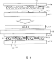
Fig. 4 is the figure that expression is connected to the panel substrate by the anisotropic conductive film of using prior art flexible substrate.
As shown in Figure 4, anisotropic conductive film 13 and flexible substrate 14 are installed on the glass substrate 11 as the chip on the film (Chip OnFilm) COF, flexible printed circuit board FPC.
Then, when flexible substrate 14 is exerted pressure, be provided with the address electrode 12 of copper Cu electrode 15 and panel substrate 11, have conducting sphere 4 between copper Cu electrode 15 and address electrode 12, wherein conducting sphere 4 is present in the anisotropic conductive film 13.
At this moment, the epoxy resin of anisotropic conductive film 13 is inserted the area of space that copper electrode 15 and address electrode 12 are not set, that is, it is formed between the copper electrode 15 and between the address electrode 12.
Thereby panel substrate 11 and flexible substrate 14 are electrically connected by conducting sphere 4, and they by between the copper electrode 15 and the epoxy resin between the address electrode 12 insulate.
But, using the anisotropic conductive film that comprises conducting sphere as mentioned above to connect under the situation of panel substrate and flexible substrate, as shown in Figure 5, when the epoxy resin of anisotropic conductive film 13 is exerted pressure, some conducting spheres that are distributed in therebetween are used for being electrically connected, and other just be pulled on one side, thereby accumulate in flexible substrate 14 ends.
Like this, the conducting sphere of gathering forms electric wire, thereby often causes short circuit.
And, in the syndeton of prior art, the panel substrate is electrically connected with flexible substrate by using conducting sphere, might be electrically connected by conducting sphere, but this conducting sphere can cause the cohesiveness of the electrode of the electrode of panel substrate and flexible substrate and die down, thereby be split in the coupling part.
Summary of the invention
Therefore, the purpose of this invention is to provide a kind of syndeton and method of attachment that is applicable to the plasma display that does not use conducting sphere and be electrically connected.
Another object of the present invention provides a kind of syndeton and method of attachment of plasma display, thereby it is applicable to that giving prominence to the electrode that inserts the panel substrate by the electrode that makes flexible substrate improves the connection cohesiveness.
In order to reach these and other objects of the present invention, the syndeton of plasma display according to an aspect of the present invention comprises first substrate with a plurality of panel electrodes; Have second substrate of a plurality of connection electrode, this connection electrode and panel electrode are arranged accordingly; And between first substrate and second substrate connector under pressure, directly connection electrode is connected with panel electrode.
In this syndeton, this connection electrode has the outstanding shape of horn shape on the connector direction.
In this syndeton, this connection electrode has the outstanding shape that has curved surface on the connector direction.
In this syndeton, this connection electrode is inserting surface plate electrode inside under pressure.
In this syndeton, second substrate is chip COF and among chip (chip-on-glass) COG on glass any one on flexible printed circuit film FPC, the film.
In this syndeton, if first substrate is a lower substrate, then panel electrode is an address electrode.
In this syndeton, if first substrate is a upper substrate, then panel electrode is a bus electrode.
In this syndeton, connector by wherein not with the epoxy resin of conducting sphere, wherein not with the styrene resin of conducting sphere, wherein not with the polyurethane resin of conducting sphere, wherein not with the phenol resin of conducting sphere with wherein not with any the making in the silicones of conducting sphere.
The method of attachment of plasma display according to a further aspect of the invention may further comprise the steps: second substrate is installed on first substrate, wherein first substrate comprises a plurality of panel electrodes, and second substrate comprises a plurality of connection electrode and by the connector of wherein not making with the resin material of conducting sphere; Connection electrode and panel electrode are aimed at, make it in correspondence with each other; By second substrate being applied the pressure that makes connection electrode insert epoxy resin, connection electrode directly is connected with panel electrode.
In this method of attachment, this connection electrode has the outstanding shape of horn shape on the connector direction.
In this method of attachment, this connection electrode has the outstanding shape that has curved surface on the connector direction.
In this method of attachment, this connection electrode inserting surface plate electrode inside.
In this method of attachment, second substrate is chip COF and among the chip COG on glass any one on flexible printed circuit film FPC, the film.
In this method of attachment, panel electrode is one of address electrode or bus electrode.
In this method of attachment, this resin material is a kind of in epoxy resin, styrene resin, polyurethane resin, phenol resin and the silicones.
Description of drawings
From below with reference to the detailed description of accompanying drawing to the embodiment of the invention, these and other purpose of the present invention will become clear, wherein:
Fig. 1 is illustrated in the figure that is electrically connected panel substrate and flexible substrate among the common PDP;
Fig. 2 is the figure that expression is bonded at the anisotropic conductive film on the flexible substrate of Fig. 1;
Fig. 3 is the figure of structure of the anisotropic conductive film of presentation graphs 2;
Fig. 4 is expression connects panel substrate and flexible substrate by the anisotropic conductive film of using prior art figure;
Fig. 5 is that expression connects by the anisotropic conductive film of using prior art under the situation of panel substrate and flexible substrate the figure that conducting sphere is assembled takes place;
Fig. 6 represents the figure of plasma display syndeton according to the preferred embodiment of the invention;
Fig. 7 is that expression connects the figure of panel substrate and flexible substrate by using anisotropic conductive film according to the preferred embodiment of the invention;
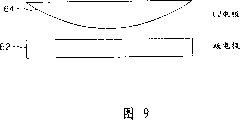
Fig. 8 is the schematic diagram that is illustrated in the shape of the copper electrode that comprises in the flexible substrate of the present invention;
Fig. 9 is another schematic diagram that is illustrated in the shape of the copper electrode that comprises in the flexible substrate of the present invention;
Figure 10 is expression and another schematic diagram of the copper electrode shape that is used for the flexible substrate that electrode pair that the present invention forms the panel of crimping shape answers.
Embodiment
To go through the preferred embodiment of the present invention now, its example illustrates in the accompanying drawings.
With reference to figure 6 to 10, will explain embodiments of the invention below.
Fig. 6 represents the figure of plasma display syndeton according to the preferred embodiment of the invention.
With reference to figure 6, preferably include panel substrate 53, flexible substrate 51 and connector 55 according to the syndeton of plasma display of the present invention.Panel substrate 53 comprises a plurality of panel electrodes 4.Flexible substrate 51 comprises a plurality of connection electrode that are provided with accordingly with panel electrode 54, as copper electrode 52.Connector 55 is between panel substrate 53 and the flexible substrate 51, and under pressure, the guiding connection electrode directly is connected with panel electrode 54 (address electrode or bus electrode).At this moment, connector 55 preferably by wherein not with the epoxy resin (epoxy resin) of conducting sphere, wherein not with the styrene resin (styreneresin) of conducting sphere, wherein not with the polyurethane resin (urethane resin) of conducting sphere, wherein not with the phenol resin (phenol resin) of conducting sphere with wherein not with any the making in the silicones (silicon resin) of conducting sphere.
Below, connector 55 is limited to anisotropic conductive film ACF and describes, still, connector of the present invention is not limited to the anisotropic conductive element, but it also can comprise the isotropism conducting film.
More particularly, panel substrate 53 can be the lower substrate or the upper substrate of plasma display.At this moment, be under the situation of lower substrate at panel substrate 53, panel electrode 54 is exactly an address electrode.And if panel substrate 53 is upper substrate, then panel electrode 54 is exactly a bus electrode.
At this moment, the copper electrode 52 that forms in the flexible substrate 51 can have outstanding (projected) shape of horn shape on the direction of anisotropic conductive film 55.That is, as shown in Figure 8, copper electrode 61 can have a plurality of triangles in the width range of panel electrode 62.At this moment, triangle can be consistent, and the perhaps middle triangle that forms can be bigger than the triangle at edge.
In addition, copper electrode 52 can have the outstanding shape that has curved surface on the direction of anisotropic conductive film 55.That is, as shown in Figure 9, copper electrode 64 can form with level and smooth curved surface (semiellipse or semicircle) outstanding, and its middle part is maximum, and diminishes gradually to both sides.
Like this, copper electrode 64 has the outstanding shape on band bending surface, therefore, its under pressure with the maximization of the contact surface of panel electrode 62, thereby farthest limit resistance components in the coupling part, thereby improve its conductive capability.
On the other hand, usually, if panel electrode 66 is formed on the panel substrate, the edge of that panel electrode 66 just forms the crimping shape.That is, the edge of panel electrode 66 forms height, and just forms low therebetween.(with reference to Figure 10)
Like this, for corresponding with panel electrode 66, copper electrode 67 forms at each mid portion 68 and 69 places, two marginal portions has the outstanding shape of horn shape, but makes the outstanding shape of mid portion 68 make greatlyyer than the outstanding shape of two marginal portions 69.
Therefore, the outstanding shape that mid portion 68 and 69 places, two marginal portions form is inserting surface plate electrode 66 as one man, thereby has more improved the connection cohesiveness.
There is the operating procedure of making above-mentioned plasma display syndeton.
Fig. 7 is that expression connects the figure of panel substrate and flexible substrate by using anisotropic conductive film according to the preferred embodiment of the invention.
At first, have the panel substrate 53 that comprises a plurality of panel electrodes 54, by anisotropic conductive film of wherein not making with the epoxy resin of conducting sphere 55 and the flexible substrate 51 that comprises a plurality of copper electrodes 52.
Anisotropic conductive film 55 and flexible substrate 51 are installed on the panel substrate 53 that provides so in order.
Next, use the alignment device (not shown) to aim at, make each panel electrode 54 corresponding with copper electrode 52.
If each panel electrode 54 is correspondingly aimed at copper electrode 52, just flexible substrate 51 is exerted pressure with hot-press equipment.
That is, press flexible substrate 51, thereby make the copper electrode 52 of flexible substrate 51 insert the epoxy resin of anisotropic conductive film 55, and be directly connected to the panel electrode 54 of panel substrate 53 with the polishing head of hot-press equipment.In other words, with to make panel electrode directly connect copper electrode by conducting sphere in the prior art different, in the present invention, owing to do not have conducting sphere in anisotropic conductive film 55, the copper electrode 52 of flexible substrate 51 inserts epoxy resin and directly connects the panel electrode 54 of panel substrate 53.
In addition, the copper electrode 52 that in this way is connected to panel electrode 54 increases along with pressure and the passage of time and gradually with the degree of depth inserting surface plate electrode 54 of appointment.At this moment, copper electrode 52 inserts and manyly therefore will not be described further deeply not within the scope of the invention, but has only in the present invention when copper electrode 52 during with the degree of depth inserting surface plate electrode 54 of appointment, realizes that the present invention does not just have obstacle.
So far, to the invention describes syndeton about plasma display, but the invention is not restricted to this, but must be noted that such fact, promptly comprise the flexible substrate of copper electrode and wherein not with the anisotropic conductive film of conducting sphere, the present invention needing to go for all displays spare of electrical connection as LCD and EL etc. with the outstanding shape of horn shape by use.
As mentioned above, used wherein not connector, thereby prevented that the conducting sphere of prior art from assembling the generation of the short circuit that causes with conducting sphere according to the syndeton of plasma display of the present invention and method of attachment.And, not using such conducting sphere, therefore can reach than the effect of more saving material in the past.
And, the copper electrode that has the flexible substrate that forms the outstanding shape of horn shape according to the syndeton of plasma display of the present invention and method of attachment, therefore copper electrode inserts the panel electrode of panel substrate, thereby has improved the connection cohesiveness between flexible substrate and the panel substrate.
Although the present invention has been described by the embodiment shown in the above-mentioned accompanying drawing, but it should be understood by one skilled in the art that, the invention is not restricted to these embodiment, but under the situation that does not break away from spirit of the present invention, might carry out variations and modifications it.Therefore, scope of the present invention can only be determined by claims and equivalent thereof.
Claims (13)
1. the syndeton of a plasma display comprises:
First substrate with a plurality of panel electrodes;
Have second substrate of a plurality of connection electrode, this connection electrode and panel electrode are arranged accordingly; And
Connector under pressure, connection electrode is connected with panel electrode between first substrate and second substrate,
Wherein this connection electrode has the outstanding shape of horn shape on this connector direction.
2, according to the syndeton of claim 1, wherein this connection electrode has the outstanding shape that has curved surface on the connector direction.
3, according to the syndeton of claim 1, this connection electrode inserting surface plate electrode inside under pressure wherein.
4, according to the syndeton of claim 1, wherein second substrate is chip and in the chip on glass any one on flexible printed circuit film, the film.
5, according to the syndeton of claim 1, if wherein first substrate is a lower substrate, then panel electrode is an address electrode.
6, according to the syndeton of claim 1, if wherein first substrate is a upper substrate, then panel electrode is a bus electrode.
7, according to the syndeton of claim 1, wherein connector by wherein not with the epoxy resin of conducting sphere, wherein not with the styrene resin of conducting sphere, wherein not with the polyurethane resin of conducting sphere, wherein not with the phenol resin of conducting sphere with wherein not with any the making in the silicones of conducting sphere.
8, a kind of method of attachment of plasma display may further comprise the steps:
Second substrate is installed on first substrate, and wherein first substrate comprises a plurality of panel electrodes, and second substrate comprises a plurality of connection electrode and by the connector of wherein not making with the resin material of conducting sphere;
Connection electrode and panel electrode are aimed at, so that it in correspondence with each other; And
By second substrate being applied the pressure that makes connection electrode insert epoxy resin, connection electrode directly is connected with panel electrode,
Wherein this connection electrode has the outstanding shape of horn shape on the connector direction.
9, method of attachment according to Claim 8, wherein this connection electrode has the outstanding shape that has curved surface on the connector direction.
10, method of attachment according to Claim 8, wherein this connection electrode inserting surface plate electrode inside.
11, method of attachment according to Claim 8, wherein second substrate is chip and in the chip on glass any one on flexible printed circuit film, the film.
12, method of attachment according to Claim 8, wherein panel electrode is one of address electrode or bus electrode.
13, method of attachment according to Claim 8, wherein this resin material is a kind of in epoxy resin, styrene resin, polyurethane resin, phenol resin and the silicones.
Applications Claiming Priority (3)
| Application Number | Priority Date | Filing Date | Title |
|---|---|---|---|
| KR46330/2003 | 2003-07-09 | ||
| KR46330/03 | 2003-07-09 | ||
| KR10-2003-0046330A KR100512992B1 (en) | 2003-07-09 | 2003-07-09 | Connection structure of plasma display panel and structure method thereof |
Publications (2)
| Publication Number | Publication Date |
|---|---|
| CN1599005A CN1599005A (en) | 2005-03-23 |
| CN100350542C true CN100350542C (en) | 2007-11-21 |
Family
ID=33448367
Family Applications (1)
| Application Number | Title | Priority Date | Filing Date |
|---|---|---|---|
| CNB2004100900054A Expired - Fee Related CN100350542C (en) | 2003-07-09 | 2004-07-09 | Connection structure and method of plasma display panel |
Country Status (5)
| Country | Link |
|---|---|
| US (1) | US7211951B2 (en) |
| EP (1) | EP1496537B1 (en) |
| JP (1) | JP2005031684A (en) |
| KR (1) | KR100512992B1 (en) |
| CN (1) | CN100350542C (en) |
Cited By (1)
| Publication number | Priority date | Publication date | Assignee | Title |
|---|---|---|---|---|
| CN104754866A (en) * | 2013-12-27 | 2015-07-01 | 昆山国显光电有限公司 | Flexible printed circuit board (FPC) and manufacture method thereof, and flat-panel display (FPD) |
Families Citing this family (9)
| Publication number | Priority date | Publication date | Assignee | Title |
|---|---|---|---|---|
| KR100718963B1 (en) * | 2005-02-17 | 2007-05-16 | 엘지전자 주식회사 | COF/TCP Electrode Unit of Plasma Display Panel |
| KR100715877B1 (en) * | 2005-09-14 | 2007-05-08 | (주)아이디에스 | flexible printed circuit having outer lead laminated prominence and depression shaped coverlay film |
| JP5128773B2 (en) * | 2006-01-23 | 2013-01-23 | 日本電気株式会社 | Manufacturing method of liquid crystal display device |
| KR100777732B1 (en) * | 2006-03-02 | 2007-11-19 | 삼성에스디아이 주식회사 | Plasma display panel |
| KR20090057719A (en) * | 2007-12-03 | 2009-06-08 | 엘지전자 주식회사 | Plasma display panel device |
| TW201123377A (en) * | 2009-12-16 | 2011-07-01 | Raydium Semiconductor Corp | Electronic chip and substrate with void |
| US10172241B2 (en) * | 2013-09-13 | 2019-01-01 | Korea Advanced Institute Of Science And Technology | Method for packaging flexible device using holding wafer, and flexible device manufactured by the same |
| EP3035117A1 (en) * | 2014-12-16 | 2016-06-22 | Gemalto Sa | Method for manufacturing a display device |
| KR20200145877A (en) * | 2019-06-19 | 2020-12-31 | 삼성디스플레이 주식회사 | Display device, manufacturing apparatus of chip on film ,and manufacturing method of chip on film |
Citations (3)
| Publication number | Priority date | Publication date | Assignee | Title |
|---|---|---|---|---|
| JPH09179505A (en) * | 1996-09-02 | 1997-07-11 | Hitachi Ltd | Flat panel display device |
| JP2000215818A (en) * | 1999-01-25 | 2000-08-04 | Nec Corp | Plasma display panel |
| JP2001351535A (en) * | 2000-06-09 | 2001-12-21 | Nec Corp | Plasma display panel and its manufacturing method |
Family Cites Families (13)
| Publication number | Priority date | Publication date | Assignee | Title |
|---|---|---|---|---|
| JPS5085297A (en) * | 1973-11-29 | 1975-07-09 | ||
| JP2827650B2 (en) * | 1992-01-14 | 1998-11-25 | 松下電器産業株式会社 | Thermocompression bonding method and crimping member |
| US5785535A (en) * | 1996-01-17 | 1998-07-28 | International Business Machines Corporation | Computer system with surface mount socket |
| JP3492195B2 (en) * | 1997-04-30 | 2004-02-03 | 松下電器産業株式会社 | Electrode bonding method for plasma display panel |
| JP2006276881A (en) * | 1997-04-30 | 2006-10-12 | Matsushita Electric Ind Co Ltd | Method for manufacturing plasma display panel |
| US6086441A (en) * | 1997-04-30 | 2000-07-11 | Matsushita Electric Industrial Co., Ltd. | Method for connecting electrodes of plasma display panel |
| JPH1140064A (en) * | 1997-07-25 | 1999-02-12 | Hitachi Ltd | Gas electric discharge display panel and display device using the same |
| JP3561137B2 (en) * | 1998-01-19 | 2004-09-02 | 株式会社エンプラス | Display panel inspection socket |
| JP3705914B2 (en) * | 1998-01-27 | 2005-10-12 | 三菱電機株式会社 | Surface discharge type plasma display panel and manufacturing method thereof |
| JPH11273577A (en) * | 1998-03-20 | 1999-10-08 | Dainippon Printing Co Ltd | Electrode terminal part of plasma display panel |
| JP3462135B2 (en) * | 1999-01-14 | 2003-11-05 | シャープ株式会社 | Two-dimensional image detector, active matrix substrate, and display device |
| JP2001305570A (en) * | 2000-04-24 | 2001-10-31 | Nec Corp | Display panel module and its manufacturing method |
| JP2002108231A (en) * | 2000-09-27 | 2002-04-10 | Fujitsu Ltd | Connection member and matrix-type display device |
-
2003
- 2003-07-09 KR KR10-2003-0046330A patent/KR100512992B1/en not_active IP Right Cessation
-
2004
- 2004-07-08 US US10/885,695 patent/US7211951B2/en not_active Expired - Fee Related
- 2004-07-09 JP JP2004203508A patent/JP2005031684A/en active Pending
- 2004-07-09 CN CNB2004100900054A patent/CN100350542C/en not_active Expired - Fee Related
- 2004-07-09 EP EP04254128A patent/EP1496537B1/en not_active Expired - Fee Related
Patent Citations (3)
| Publication number | Priority date | Publication date | Assignee | Title |
|---|---|---|---|---|
| JPH09179505A (en) * | 1996-09-02 | 1997-07-11 | Hitachi Ltd | Flat panel display device |
| JP2000215818A (en) * | 1999-01-25 | 2000-08-04 | Nec Corp | Plasma display panel |
| JP2001351535A (en) * | 2000-06-09 | 2001-12-21 | Nec Corp | Plasma display panel and its manufacturing method |
Cited By (2)
| Publication number | Priority date | Publication date | Assignee | Title |
|---|---|---|---|---|
| CN104754866A (en) * | 2013-12-27 | 2015-07-01 | 昆山国显光电有限公司 | Flexible printed circuit board (FPC) and manufacture method thereof, and flat-panel display (FPD) |
| CN104754866B (en) * | 2013-12-27 | 2019-01-04 | 昆山国显光电有限公司 | Flexible printed circuit board and its manufacturing method and flat-panel monitor |
Also Published As
| Publication number | Publication date |
|---|---|
| JP2005031684A (en) | 2005-02-03 |
| US7211951B2 (en) | 2007-05-01 |
| EP1496537A2 (en) | 2005-01-12 |
| EP1496537A3 (en) | 2007-07-25 |
| KR20050006496A (en) | 2005-01-17 |
| KR100512992B1 (en) | 2005-09-05 |
| US20050006650A1 (en) | 2005-01-13 |
| EP1496537B1 (en) | 2013-01-09 |
| CN1599005A (en) | 2005-03-23 |
Similar Documents
| Publication | Publication Date | Title |
|---|---|---|
| CN1196957C (en) | LCD device | |
| CN1184508C (en) | Liquid crystal display device with flexible circuit board | |
| CN1292290C (en) | Method for making liquid crystal display combined with film type touch board | |
| CN1227735C (en) | Installation structure of semi-conductor apparatus, electro-optical apparatus and electronic apparatus | |
| CN100350542C (en) | Connection structure and method of plasma display panel | |
| CN1477425A (en) | Liquid crystal display | |
| CN1505455A (en) | Interconnection structure of electric conductive wirings | |
| CN1913117A (en) | Method for improving electron circuit layout efficiency, electronic connector and electronic panel | |
| CN1237383C (en) | Liquid crystal display | |
| CN1741100A (en) | Display apparatus | |
| CN1693954A (en) | Display device | |
| CN1607895A (en) | Flexible printed circuit board and liquid crystal display having the same | |
| CN1805672A (en) | Plasma display device with grounding module | |
| CN1655661A (en) | Mounting structure, electro-optical device, electronic apparatus, and method of manufacturing electro-optical device | |
| CN1811864A (en) | Flat panel display and method of fabricating the same | |
| CN1753603A (en) | Electronic component-mounted structure, method for mounting electronic component, electro-optical device, and electronic apparatus | |
| CN1629917A (en) | Drive chip and display device with the same | |
| CN1955794A (en) | Liquid crystal display device | |
| CN1808712A (en) | Semiconductor device, display module, and manufacturing method of semiconductor device | |
| CN1624733A (en) | Interconnector, method for manufacturing a plasma display device using the same, and a plasma display device with the same | |
| CN1855631A (en) | Connector and printed circuit board connected to the same | |
| CN1801252A (en) | Plasma display apparatus | |
| CN1612183A (en) | Plasma display apparatus | |
| CN1761382A (en) | Plasma display device | |
| CN1976557A (en) | Circuit board device and method for board-to-board connection |
Legal Events
| Date | Code | Title | Description |
|---|---|---|---|
| C06 | Publication | ||
| PB01 | Publication | ||
| C10 | Entry into substantive examination | ||
| SE01 | Entry into force of request for substantive examination | ||
| C14 | Grant of patent or utility model | ||
| GR01 | Patent grant | ||
| CF01 | Termination of patent right due to non-payment of annual fee |
Granted publication date: 20071121 Termination date: 20140709 |
|
| EXPY | Termination of patent right or utility model |