JP2005031684A - Connection structure and method of plasma display panel - Google Patents
Connection structure and method of plasma display panel Download PDFInfo
- Publication number
- JP2005031684A JP2005031684A JP2004203508A JP2004203508A JP2005031684A JP 2005031684 A JP2005031684 A JP 2005031684A JP 2004203508 A JP2004203508 A JP 2004203508A JP 2004203508 A JP2004203508 A JP 2004203508A JP 2005031684 A JP2005031684 A JP 2005031684A
- Authority
- JP
- Japan
- Prior art keywords
- electrode
- panel
- connection
- substrate
- plasma display
- Prior art date
- Legal status (The legal status is an assumption and is not a legal conclusion. Google has not performed a legal analysis and makes no representation as to the accuracy of the status listed.)
- Pending
Links
Images


Classifications
-
- H—ELECTRICITY
- H01—ELECTRIC ELEMENTS
- H01J—ELECTRIC DISCHARGE TUBES OR DISCHARGE LAMPS
- H01J11/00—Gas-filled discharge tubes with alternating current induction of the discharge, e.g. alternating current plasma display panels [AC-PDP]; Gas-filled discharge tubes without any main electrode inside the vessel; Gas-filled discharge tubes with at least one main electrode outside the vessel
- H01J11/20—Constructional details
- H01J11/46—Connecting or feeding means, e.g. leading-in conductors
-
- H—ELECTRICITY
- H01—ELECTRIC ELEMENTS
- H01J—ELECTRIC DISCHARGE TUBES OR DISCHARGE LAMPS
- H01J11/00—Gas-filled discharge tubes with alternating current induction of the discharge, e.g. alternating current plasma display panels [AC-PDP]; Gas-filled discharge tubes without any main electrode inside the vessel; Gas-filled discharge tubes with at least one main electrode outside the vessel
- H01J11/10—AC-PDPs with at least one main electrode being out of contact with the plasma
- H01J11/12—AC-PDPs with at least one main electrode being out of contact with the plasma with main electrodes provided on both sides of the discharge space
-
- H—ELECTRICITY
- H01—ELECTRIC ELEMENTS
- H01J—ELECTRIC DISCHARGE TUBES OR DISCHARGE LAMPS
- H01J11/00—Gas-filled discharge tubes with alternating current induction of the discharge, e.g. alternating current plasma display panels [AC-PDP]; Gas-filled discharge tubes without any main electrode inside the vessel; Gas-filled discharge tubes with at least one main electrode outside the vessel
- H01J11/20—Constructional details
- H01J11/22—Electrodes, e.g. special shape, material or configuration
-
- H—ELECTRICITY
- H01—ELECTRIC ELEMENTS
- H01R—ELECTRICALLY-CONDUCTIVE CONNECTIONS; STRUCTURAL ASSOCIATIONS OF A PLURALITY OF MUTUALLY-INSULATED ELECTRICAL CONNECTING ELEMENTS; COUPLING DEVICES; CURRENT COLLECTORS
- H01R12/00—Structural associations of a plurality of mutually-insulated electrical connecting elements, specially adapted for printed circuits, e.g. printed circuit boards [PCB], flat or ribbon cables, or like generally planar structures, e.g. terminal strips, terminal blocks; Coupling devices specially adapted for printed circuits, flat or ribbon cables, or like generally planar structures; Terminals specially adapted for contact with, or insertion into, printed circuits, flat or ribbon cables, or like generally planar structures
- H01R12/50—Fixed connections
- H01R12/51—Fixed connections for rigid printed circuits or like structures
- H01R12/52—Fixed connections for rigid printed circuits or like structures connecting to other rigid printed circuits or like structures
-
- H—ELECTRICITY
- H01—ELECTRIC ELEMENTS
- H01R—ELECTRICALLY-CONDUCTIVE CONNECTIONS; STRUCTURAL ASSOCIATIONS OF A PLURALITY OF MUTUALLY-INSULATED ELECTRICAL CONNECTING ELEMENTS; COUPLING DEVICES; CURRENT COLLECTORS
- H01R12/00—Structural associations of a plurality of mutually-insulated electrical connecting elements, specially adapted for printed circuits, e.g. printed circuit boards [PCB], flat or ribbon cables, or like generally planar structures, e.g. terminal strips, terminal blocks; Coupling devices specially adapted for printed circuits, flat or ribbon cables, or like generally planar structures; Terminals specially adapted for contact with, or insertion into, printed circuits, flat or ribbon cables, or like generally planar structures
- H01R12/70—Coupling devices
- H01R12/7076—Coupling devices for connection between PCB and component, e.g. display
-
- H—ELECTRICITY
- H01—ELECTRIC ELEMENTS
- H01R—ELECTRICALLY-CONDUCTIVE CONNECTIONS; STRUCTURAL ASSOCIATIONS OF A PLURALITY OF MUTUALLY-INSULATED ELECTRICAL CONNECTING ELEMENTS; COUPLING DEVICES; CURRENT COLLECTORS
- H01R13/00—Details of coupling devices of the kinds covered by groups H01R12/70 or H01R24/00 - H01R33/00
- H01R13/02—Contact members
- H01R13/22—Contacts for co-operating by abutting
-
- H—ELECTRICITY
- H01—ELECTRIC ELEMENTS
- H01R—ELECTRICALLY-CONDUCTIVE CONNECTIONS; STRUCTURAL ASSOCIATIONS OF A PLURALITY OF MUTUALLY-INSULATED ELECTRICAL CONNECTING ELEMENTS; COUPLING DEVICES; CURRENT COLLECTORS
- H01R4/00—Electrically-conductive connections between two or more conductive members in direct contact, i.e. touching one another; Means for effecting or maintaining such contact; Electrically-conductive connections having two or more spaced connecting locations for conductors and using contact members penetrating insulation
- H01R4/26—Connections in which at least one of the connecting parts has projections which bite into or engage the other connecting part in order to improve the contact
-
- H—ELECTRICITY
- H05—ELECTRIC TECHNIQUES NOT OTHERWISE PROVIDED FOR
- H05K—PRINTED CIRCUITS; CASINGS OR CONSTRUCTIONAL DETAILS OF ELECTRIC APPARATUS; MANUFACTURE OF ASSEMBLAGES OF ELECTRICAL COMPONENTS
- H05K3/00—Apparatus or processes for manufacturing printed circuits
- H05K3/36—Assembling printed circuits with other printed circuits
- H05K3/361—Assembling flexible printed circuits with other printed circuits
-
- H—ELECTRICITY
- H01—ELECTRIC ELEMENTS
- H01L—SEMICONDUCTOR DEVICES NOT COVERED BY CLASS H10
- H01L2224/00—Indexing scheme for arrangements for connecting or disconnecting semiconductor or solid-state bodies and methods related thereto as covered by H01L24/00
- H01L2224/73—Means for bonding being of different types provided for in two or more of groups H01L2224/10, H01L2224/18, H01L2224/26, H01L2224/34, H01L2224/42, H01L2224/50, H01L2224/63, H01L2224/71
- H01L2224/732—Location after the connecting process
- H01L2224/73201—Location after the connecting process on the same surface
- H01L2224/73203—Bump and layer connectors
- H01L2224/73204—Bump and layer connectors the bump connector being embedded into the layer connector
-
- H—ELECTRICITY
- H05—ELECTRIC TECHNIQUES NOT OTHERWISE PROVIDED FOR
- H05K—PRINTED CIRCUITS; CASINGS OR CONSTRUCTIONAL DETAILS OF ELECTRIC APPARATUS; MANUFACTURE OF ASSEMBLAGES OF ELECTRICAL COMPONENTS
- H05K2201/00—Indexing scheme relating to printed circuits covered by H05K1/00
- H05K2201/03—Conductive materials
- H05K2201/0332—Structure of the conductor
- H05K2201/0364—Conductor shape
- H05K2201/0367—Metallic bump or raised conductor not used as solder bump
-
- H—ELECTRICITY
- H05—ELECTRIC TECHNIQUES NOT OTHERWISE PROVIDED FOR
- H05K—PRINTED CIRCUITS; CASINGS OR CONSTRUCTIONAL DETAILS OF ELECTRIC APPARATUS; MANUFACTURE OF ASSEMBLAGES OF ELECTRICAL COMPONENTS
- H05K3/00—Apparatus or processes for manufacturing printed circuits
- H05K3/30—Assembling printed circuits with electric components, e.g. with resistor
- H05K3/32—Assembling printed circuits with electric components, e.g. with resistor electrically connecting electric components or wires to printed circuits
- H05K3/321—Assembling printed circuits with electric components, e.g. with resistor electrically connecting electric components or wires to printed circuits by conductive adhesives
- H05K3/323—Assembling printed circuits with electric components, e.g. with resistor electrically connecting electric components or wires to printed circuits by conductive adhesives by applying an anisotropic conductive adhesive layer over an array of pads
Abstract
Description
本発明はプラズマディスプレイパネル装置に関し、特にプラズマディスプレイパネル装置においてパネル基板と印刷回路基板(PCB)とを接続部材を介して電気的に連結する接続構造及び接続方法に関する。 The present invention relates to a plasma display panel device, and more particularly to a connection structure and a connection method for electrically connecting a panel substrate and a printed circuit board (PCB) through a connecting member in the plasma display panel device.
最近、情報処理システムの発達と普及に伴って映像情報の重要性が増大している。このような映像情報の最も重要なマン−マシン・インターフェースとして、ディスプレイ手段が重要になっている。 Recently, the importance of video information has increased with the development and popularization of information processing systems. Display means are important as the most important man-machine interface for such video information.
ディスプレイ手段はLCDやTV、AVのモニター、コンピューターディスプレイなどに適用することができる。このようなディスプレイ手段の中でプラズマディスプレイパネル(PDP)は厚さが薄くて軽くて大型化が可能であるという長所がある。 The display means can be applied to LCDs, TVs, AV monitors, computer displays, and the like. Among such display means, the plasma display panel (PDP) has an advantage that it is thin and light and can be enlarged.
PDPは放電を発生するパネル、そのパネルを制御する駆動回路を備える印刷回路基板、その他の放熱装置などをセットに含んでいる。 The PDP includes a panel that generates a discharge, a printed circuit board that includes a drive circuit that controls the panel, and other heat dissipation devices.
パネルと印刷回路基板の間は、異方性導電フィルム(ACF:Anisotropic Conductive Film)で電気的に連結されている。 The panel and the printed circuit board are electrically connected by an anisotropic conductive film (ACF).
図1は一般的なPDPでパネル基板と印刷回路基板としてのフレキシブル基板との電気的な連結状態を示している。図2は図1でフレキシブル基板に取り付ける異方性導電フィルムを示している。図3は図2の異方性導電フィルムの構造を示す図である。 FIG. 1 shows an electrical connection between a panel substrate and a flexible substrate as a printed circuit board in a general PDP. FIG. 2 shows an anisotropic conductive film attached to the flexible substrate in FIG. FIG. 3 is a view showing the structure of the anisotropic conductive film of FIG.
図1〜3を参照すると、矩形平面状のパネル基板(1)に信号の連結のために多数のフレキシブル基板(2)が取り付けられている。パネル基板(1)にフレキシブル基板(2)を接着させるために、フレキシブル基板(2)の端部に異方性導電フィルム(3)を付着させ、そのフィルムを付着させた端部をパネル基板(1)の周辺部に固定し、同時に電気的にも連結させている。 1 to 3, a large number of flexible substrates (2) are attached to a rectangular planar panel substrate (1) for signal connection. In order to adhere the flexible substrate (2) to the panel substrate (1), the anisotropic conductive film (3) is attached to the end of the flexible substrate (2), and the end to which the film is attached is attached to the panel substrate ( It is fixed to the periphery of 1) and is also electrically connected at the same time.
ここで使用される異方性導電フィルム(3)は図3に示したように導電ボール(4)を含むエポキシ樹脂(5)のからなる。ここで符号(6)は異方性導電フィルム(3)を保護するためのPET樹脂である。 The anisotropic conductive film (3) used here consists of an epoxy resin (5) containing a conductive ball (4) as shown in FIG. Here, reference numeral (6) denotes a PET resin for protecting the anisotropic conductive film (3).
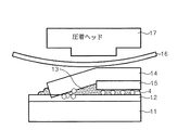
図4は異方性導電フィルムを利用してパネル基板とフレキシブル基板とを接続させる従来の方法を示す図である。 FIG. 4 is a view showing a conventional method of connecting a panel substrate and a flexible substrate using an anisotropic conductive film.
図4に示したように、ガラス基板(11)上に異方性導電フィルム(13)とフレキシブル基板(14)、例えばCOF(Chip On Film)やFPC(Flexible Printed Circuit Film)を順に取り付ける。 As shown in FIG. 4, an anisotropic conductive film (13) and a flexible substrate (14) such as COF (Chip On Film) and FPC (Flexible Printed Circuit Film) are sequentially attached on a glass substrate (11).
このように取り付けられたフレキシブル基板(14)上にシリコーンラバー(16)を載せて、圧着装置(図示しない)の熱圧着ヘッド(17)を利用してフレキシブル基板(14)を押圧させる。シリコーンラバー(16)は圧着装置の押圧によってパネル基板(11)が損傷されるのを防ぐための緩衝材である。 A silicone rubber (16) is placed on the flexible substrate (14) attached in this manner, and the flexible substrate (14) is pressed using a thermocompression bonding head (17) of a pressure bonding device (not shown). The silicone rubber (16) is a cushioning material for preventing the panel substrate (11) from being damaged by the pressure of the crimping device.
フレキシブル基板(14)が押圧されると、フレキシブル基板(14)に設けられている電極(15)とガラス基板に電極(15)に向き合うように設けられているアドレス電極(12)が接近し、その間にある異方性導電フィルム(13)に存在する導電ボール(4)が銅(Cu)からなる電極(15)とパネル基板(11)のアドレス電極(12)との間に介在して両者を電気的に結合させるようになる。 When the flexible substrate (14) is pressed, the electrode (15) provided on the flexible substrate (14) and the address electrode (12) provided to face the electrode (15) approach the glass substrate, The conductive ball (4) existing in the anisotropic conductive film (13) between them is interposed between the electrode (15) made of copper (Cu) and the address electrode (12) of the panel substrate (11). Are electrically coupled.
一方、隣接する銅電極(15)どうしの間と、同様に隣り合っているアドレス電極(12)の間に形成される空間領域には異方性導電フィルム(13)のエポキシ樹脂が満たされる。 On the other hand, the space region formed between adjacent copper electrodes (15) and similarly between adjacent address electrodes (12) is filled with the epoxy resin of the anisotropic conductive film (13).
したがって、パネル基板(11)とフレキシブル基板(14)の電極の間は導電ボール(4)によって電気的に連結される一方、隣合う銅電極(15)の間及び隣合うアドレス電極(12)の間はエポキシ樹脂によって絶縁される。 Accordingly, the electrodes of the panel substrate (11) and the flexible substrate (14) are electrically connected by the conductive balls (4), while between the adjacent copper electrodes (15) and between the adjacent address electrodes (12). The space is insulated by epoxy resin.
しかし、前記のように導電ボールを含む異方性導電フィルムを使ってパネル基板とフレキシブル基板を接続する場合には、図5に示したように、押圧されたときに異方性導電フィルム(13)のエポキシ樹脂が押されて、その中に分散していた導電ボール(4)の一部は電極の電気的連結のために使われるが、他の一部は横に押されてフレキシブル基板(14)の端部に集まることがある。 However, when the panel substrate and the flexible substrate are connected using the anisotropic conductive film including the conductive balls as described above, the anisotropic conductive film (13) is pressed when pressed as shown in FIG. ) Epoxy resin is pressed and a part of the conductive balls (4) dispersed therein are used for electrical connection of the electrodes, while the other part is pressed sideways to the flexible substrate ( 14).
このように集まった導電ボールが電気的ラインを形成して電気的にショートさせることがあるという問題があった。 There is a problem that the conductive balls gathered in this way may form an electrical line and be electrically short-circuited.
また、導電ボールを利用してパネル基板とフレキシブル基板の間の電気的な連結をする従来の接続構造では、導電ボールによって電気的な連結はできるものの、このような導電ボールのためパネル基板の電極とフレキシブル基板の電極の結合力が弱くなって接続部分が離脱する可能性が高かった。 In addition, in the conventional connection structure in which the electrical connection is made between the panel substrate and the flexible substrate using the conductive ball, the electrical connection can be made by the conductive ball. There was a high possibility that the connection of the electrodes of the flexible board would be weakened and the connection part would be detached.
したがって、本発明は導電ボールを使わないで電気的な接続が可能なプラズマディスプレイパネルの接続構造及び接続方法を提供することを目的にする。 Accordingly, it is an object of the present invention to provide a plasma display panel connection structure and a connection method capable of electrical connection without using conductive balls.
本発明の他の目的は、フレキシブル基板の電極を突き出させてパネル基板の電極へ差し込まれるようにすることで、接続結合力を高めることができるプラズマディスプレイパネルの接続構造及び接続方法を提供することである。 Another object of the present invention is to provide a plasma display panel connection structure and a connection method capable of increasing the connection coupling force by protruding the electrode of the flexible substrate and inserting it into the electrode of the panel substrate. It is.
上記目的を達成するために、本発明のプラズマディスプレイパネルの接続構造は、複数のパネル用電極を備える第1基板と、その複数のパネル用電極と対応されるように配列された複数の接続用電極を備える第2基板と、第1基板と第2基板の間に配置され、押圧されたとき接続用電極がパネル用電極に直接連結されるように導く接続部材を含む。 To achieve the above object, a plasma display panel connection structure of the present invention includes a first substrate having a plurality of panel electrodes and a plurality of connection arrays arranged to correspond to the plurality of panel electrodes. A second substrate provided with an electrode; and a connecting member disposed between the first substrate and the second substrate and guiding the connection electrode so as to be directly coupled to the panel electrode when pressed.
前記接続用電極は前記接続部材方向に先端が先鋭にされるかまたは曲面を有する突出形状からなる。 The connection electrode has a protruding shape having a sharp tip or a curved surface in the direction of the connection member.
前記接続用電極は押圧されたとき、パネル用電極の内部に入り込むことができる。 When the connection electrode is pressed, the connection electrode can enter the panel electrode.
本発明の望ましい他の実施態様によると、プラズマディスプレイパネルの接続方法は、複数のパネル用電極を備えた第1基板上に、導電ボールが存在しない樹脂材質からなる接続部材と複数の接続用電極を備えた第2基板を順に重ねる段階と、前記複数の接続用電極と前記複数のパネル用電極のそれぞれが対応するようにアラインさせる段階と、前記第2基板を押圧して前記複数の接続用電極を、前記エポキシ樹脂を貫いて前記複数のパネル用電極と直接的に連結させる段階とを含む。 According to another preferred embodiment of the present invention, a plasma display panel connection method includes a connection member made of a resin material having no conductive ball on a first substrate having a plurality of panel electrodes and a plurality of connection electrodes. A step of sequentially stacking a second substrate having a plurality of connection electrodes, a step of aligning the plurality of connection electrodes and the plurality of panel electrodes to correspond to each other, and pressing the second substrate to connect the plurality of connection electrodes. Directly connecting the electrode with the plurality of panel electrodes through the epoxy resin.
本発明に係るプラズマディスプレイパネルの接続構造及び接続方法によると、導電ボールが存在しない接続部材を使うので、従来のように、導電ボールが集まってショートするのを防止することができる。また、このように導電ボールを使わないので、材料費がより節減される效果がある。 According to the connection structure and connection method of the plasma display panel according to the present invention, since the connection member having no conductive ball is used, it is possible to prevent the conductive balls from being collected and short-circuited as in the related art. Further, since the conductive balls are not used in this way, there is an effect that the material cost is further reduced.
また、本発明のプラズマディスプレイパネルの接続構造及び接続方法によると、フレキシブル基板の銅電極を先端を先鋭にした突出形状に形成して銅電極がパネル基板のパネル用電極に差し込まれるようにしたので、フレキシブル基板とパネル基板の間の接続結合力をより高めることができるという效果がある。 Also, according to the plasma display panel connection structure and connection method of the present invention, the copper electrode of the flexible substrate is formed in a protruding shape with a sharpened tip so that the copper electrode is inserted into the panel electrode of the panel substrate. There is an effect that it is possible to further increase the connection and coupling force between the flexible substrate and the panel substrate.
以下、添付された図面を参照して本発明に係るプラズマディスプレイパネルに対して詳しく説明する。 Hereinafter, a plasma display panel according to the present invention will be described in detail with reference to the accompanying drawings.
図6は本発明の望ましい実施形態に係るプラズマディスプレイパネルの接続構造を示す図である。 FIG. 6 is a view illustrating a connection structure of a plasma display panel according to a preferred embodiment of the present invention.
図6を参照すると、本発明に係るプラズマディスプレイパネルの接続構造はパネル基板(53)と、フレキシブル基板(51)と、接続部材(55)とを含んでいる。パネル基板(53)は複数のパネル用電極(54)を備え、フレキシブル基板(51)はパネル基板(53)の複数のパネル用電極(54)と対応するように配列された複数の接続用電極(例えば、銅電極(52))を備えている。接続部材(55)はパネル基板(53)とフレキシブル基板(51)との間に配置され、押圧されたときに接続用電極がパネル用電極(54)(アドレス電極またはバス電極)に直接連結されるように導く構成とされている。この接続部材(55)の材料としてはエポキシ樹脂、スチレン樹脂、ウレタン樹脂、フェノール樹脂、シリコーン樹脂などからなることが望ましい。そして、いずれの材料からなるにしてもそれには従来のような導電ボールは含まれない。 Referring to FIG. 6, the plasma display panel connection structure according to the present invention includes a panel substrate (53), a flexible substrate (51), and a connection member (55). The panel substrate (53) includes a plurality of panel electrodes (54), and the flexible substrate (51) is a plurality of connection electrodes arranged so as to correspond to the plurality of panel electrodes (54) of the panel substrate (53). (For example, a copper electrode (52)). The connection member (55) is disposed between the panel substrate (53) and the flexible substrate (51), and when pressed, the connection electrode is directly coupled to the panel electrode (54) (address electrode or bus electrode). It is set as the structure which guides as follows. The connecting member (55) is preferably made of epoxy resin, styrene resin, urethane resin, phenol resin, silicone resin, or the like. And it does not include a conventional conductive ball, regardless of which material is used.
より詳しく説明すると、パネル基板(53)はプラズマディスプレイパネルの下部基板または上部基板である。パネル基板(53)が下部基板の場合、パネル用電極(54)はアドレス電極を意味し、パネル基板(53)が上部基板の場合、パネル用電極(54)はバス電極を意味する。 More specifically, the panel substrate (53) is a lower substrate or an upper substrate of the plasma display panel. When the panel substrate (53) is a lower substrate, the panel electrode (54) means an address electrode, and when the panel substrate (53) is an upper substrate, the panel electrode (54) means a bus electrode.
回路基板としてのフレキシブル基板(51)は、フレキシブル印刷回路フィルム(FPC:Flexible Printed Circuit Film)、チップオンフィルム(COF:Chip On Film)、チップオンガラス(COG:Chip On Glass)のいずれか一つとすることができる。 The flexible substrate (51) as a circuit substrate is one of a flexible printed circuit film (FPC), a chip on film (COF), and a chip on glass (COG). can do.
フレキシブル基板(51)に形成される銅からなる接続用電極(52)は接続部材(55)に向かって突出した突出形状とされている。しかも、その先端が図示のように先鋭にされている。その例としては、例えば図8に示したように、パネル用電極(62)の幅内で複数の先端を持たせた山の形状とすることもできる。この山の形状は、全て同じ形状とすることもでき、あるいは、中心部の山の形状が両端部分の山の形状より大きく形成することもできる。 The connection electrode (52) made of copper formed on the flexible substrate (51) has a protruding shape protruding toward the connection member (55). In addition, the tip is sharpened as shown. As an example thereof, as shown in FIG. 8, for example, a mountain shape having a plurality of tips within the width of the panel electrode (62) may be used. The shape of the peaks can be all the same, or the shape of the peaks at the center can be larger than the shape of the peaks at both ends.
このように先端を先鋭にされた突出形状の銅電極(61)は押圧されたときに対応するパネル用電極(62)に差し込まれ、パネル用電極(62)と銅電極(61)とが直接接触するとともに、その接続結合力をより高めることができ、従来技術でのように結合力が弱くてパネル基板とフレキシブル基板が離れることを防止することができる。 The protruding copper electrode (61) with the sharpened tip is inserted into the corresponding panel electrode (62) when pressed, and the panel electrode (62) and the copper electrode (61) are directly connected. In addition to the contact, the connection / bonding force can be further increased, and it is possible to prevent the panel substrate and the flexible substrate from separating due to the weak bonding force as in the prior art.
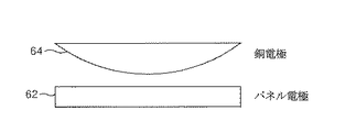
また、銅電極(52)は接続部材(55)の方向に湾曲した突出形状とすることもできる。すなわち、図9に示したように、銅電極(64)は中心部が一番大きくて端に行くほど次第に小くなる柔らかい曲面(半楕円または半円)として突き出るように形成されてもよい。 Moreover, the copper electrode (52) can also be made into the protrusion shape curved in the direction of the connection member (55). That is, as shown in FIG. 9, the copper electrode (64) may be formed so as to protrude as a soft curved surface (semi-ellipse or semi-circle) whose center portion is the largest and gradually decreases toward the end.
このように銅電極(64)が曲面を有する突出形状からなると、押圧されたときパネル用電極(62)との接触面積を最大限拡大することができ、接続部分での電気的な抵抗成分を最大限抑制して導電性を高めることができる。 When the copper electrode (64) has a curved shape as described above, the contact area with the panel electrode (62) can be maximized when pressed, and the electrical resistance component at the connection portion can be reduced. The conductivity can be increased with maximum suppression.
一方、パネル基板上にパネル用電極(66)を形成すると、パネル用電極(66)はその端がエッジカール形態となるように形成される。すなわち、パネル用電極(66)の端が高く形成され、中心部がより低くなるように形成される(図10参照)。 On the other hand, when the panel electrode (66) is formed on the panel substrate, the end of the panel electrode (66) is formed in an edge curl shape. That is, the end of the panel electrode (66) is formed high and the center is formed lower (see FIG. 10).
このようなパネル用電極(66)に対応するために銅電極(67)は中心部(68)と両端部(69)のそれぞれを先端を先鋭にした突出形状から形成するが、中心部(68)の突出形状が両方端(69)の突出形状より大きくすることが望ましい。 In order to cope with such a panel electrode (66), the copper electrode (67) is formed in a projecting shape with a sharpened tip at each of the center (68) and both ends (69). It is desirable that the protruding shape of) be larger than the protruding shape of both ends (69).
そのようにすることで、エッジカール形態となったパネル用電極に対して中心部(68)も両方端部(69)もそれぞれに形成された突出形状がパネル用電極(66)にほぼ等しい深さに入り込み、より接続結合力を高めることができる。 By doing so, the protruding shape formed in each of the center portion (68) and both end portions (69) with respect to the panel electrode in the edge curl form has a depth substantially equal to that of the panel electrode (66). It is possible to increase the connecting force.
前記したプラズマディスプレイの接続構造を形成するための動作過程を説明する。 An operation process for forming the connection structure of the plasma display will be described.
図7は本発明の望ましい実施形態による接続部材を利用してパネル基板とフレキシブル基板を接続させる状態を示した図である。 FIG. 7 is a view illustrating a state in which the panel substrate and the flexible substrate are connected using the connection member according to the preferred embodiment of the present invention.
最初に、複数のパネル用電極(54)を設けたパネル基板(53)と、導電ボールが存在しないエポキシ樹脂からなる接続部材(55)と、複数の銅電極(52)を設けけたフレキシブル基板(51)とを用意する。 First, a panel substrate (53) provided with a plurality of panel electrodes (54), a connection member (55) made of an epoxy resin having no conductive ball, and a flexible substrate provided with a plurality of copper electrodes (52) ( 51).
このように用意されたパネル基板(53)の上に接続部材(55)とフレキシブル基板(51)を順に積層させる。 The connection member (55) and the flexible substrate (51) are sequentially laminated on the panel substrate (53) prepared in this manner.
次に、複数の銅電極(52)と複数のパネル用電極(54)のそれぞれが対応するようにアライン装置(図示しない)などを利用してアラインが行われる。 Next, alignment is performed using an aligner (not shown) or the like so that the plurality of copper electrodes (52) and the plurality of panel electrodes (54) correspond to each other.
アラインによって複数の銅電極(52)と複数のパネル用電極(54)がそれぞれ対応して一致すると、熱圧着装置を利用してフレキシブル基板(51)を押圧させる。 When the plurality of copper electrodes (52) and the plurality of panel electrodes (54) are correspondingly matched by the alignment, the flexible substrate (51) is pressed using a thermocompression bonding device.
すなわち、熱圧着装置の圧着ヘッドによってフレキシブル基板(51)が押され、これによってフレキシブル基板(51)の銅電極(52)が接続部材(55)のエポキシ樹脂を貫いてパネル基板(53)のパネル用電極(54)と直接的に連結される。すなわち、従来は導電ボールによってパネル用電極と銅電極が間接的に連結されていたのに比べて、本発明では接続部材(55)に導電ボールがないので、フレキシブル基板(51)の銅電極(52)がエポキシ樹脂を貫いてパネル基板(53)のパネル用電極(54)と直接連結される。 That is, the flexible substrate (51) is pushed by the pressure bonding head of the thermocompression bonding device, whereby the copper electrode (52) of the flexible substrate (51) penetrates the epoxy resin of the connecting member (55) and the panel of the panel substrate (53). Directly connected to the working electrode (54). That is, compared with the case where the panel electrode and the copper electrode are indirectly connected by the conductive ball conventionally, the connection member (55) does not have the conductive ball in the present invention, so the copper electrode of the flexible substrate (51) ( 52) penetrates the epoxy resin and is directly connected to the panel electrode (54) of the panel substrate (53).
それだけでなく、このようにパネル用電極(54)に連結される銅電極(52)は圧力が増加して時間が経過するのに伴って次第にパネル用電極(54)で所定の深さだけ入り込む。この時、銅電極(52)をどの程度の深さ入り込ませるかに対しては本発明の範囲を越すのでこれ以上説明しない。本発明では銅電極(52)がパネル用電極(54)に対して所定の深さだけ入り込みさえすればよい。 In addition, the copper electrode (52) connected to the panel electrode (54) in this manner gradually enters the panel electrode (54) to a predetermined depth as time increases and the time elapses. . At this time, the depth of penetration of the copper electrode (52) is beyond the scope of the present invention and will not be described further. In the present invention, the copper electrode (52) has only to enter a predetermined depth with respect to the panel electrode (54).
今まで本発明はプラズマディスプレイパネルの接続構造に対して説明したが、本発明はこれに限定されず、導電ボールが存在しない接続部材と先端が先鋭にされた突出形状を有する銅電極を具備したフレキシブル基板を利用して電気的連結をしようとするすべてのディスプレイ素子、例えば LCD、ELなどにも適用することができる。 Although the present invention has been described so far with respect to the connection structure of the plasma display panel, the present invention is not limited thereto, and includes a connection member having no conductive ball and a copper electrode having a protruding shape with a sharp tip. The present invention can also be applied to all display elements that are to be electrically connected using a flexible substrate, such as LCDs and ELs.
51:フレキシブル基板、52:銅電極、53:パネル基板、54:パネル用電極、55:接続部材 51: Flexible substrate, 52: Copper electrode, 53: Panel substrate, 54: Panel electrode, 55: Connection member
Claims (15)
Applications Claiming Priority (1)
| Application Number | Priority Date | Filing Date | Title |
|---|---|---|---|
| KR10-2003-0046330A KR100512992B1 (en) | 2003-07-09 | 2003-07-09 | Connection structure of plasma display panel and structure method thereof |
Publications (2)
| Publication Number | Publication Date |
|---|---|
| JP2005031684A true JP2005031684A (en) | 2005-02-03 |
| JP2005031684A5 JP2005031684A5 (en) | 2007-08-23 |
Family
ID=33448367
Family Applications (1)
| Application Number | Title | Priority Date | Filing Date |
|---|---|---|---|
| JP2004203508A Pending JP2005031684A (en) | 2003-07-09 | 2004-07-09 | Connection structure and method of plasma display panel |
Country Status (5)
| Country | Link |
|---|---|
| US (1) | US7211951B2 (en) |
| EP (1) | EP1496537B1 (en) |
| JP (1) | JP2005031684A (en) |
| KR (1) | KR100512992B1 (en) |
| CN (1) | CN100350542C (en) |
Cited By (1)
| Publication number | Priority date | Publication date | Assignee | Title |
|---|---|---|---|---|
| JP2006227622A (en) * | 2005-02-17 | 2006-08-31 | Lg Electronics Inc | Plasma display device including connector |
Families Citing this family (9)
| Publication number | Priority date | Publication date | Assignee | Title |
|---|---|---|---|---|
| KR100715877B1 (en) * | 2005-09-14 | 2007-05-08 | (주)아이디에스 | flexible printed circuit having outer lead laminated prominence and depression shaped coverlay film |
| JP5128773B2 (en) * | 2006-01-23 | 2013-01-23 | 日本電気株式会社 | Manufacturing method of liquid crystal display device |
| KR100777732B1 (en) * | 2006-03-02 | 2007-11-19 | 삼성에스디아이 주식회사 | Plasma display panel |
| KR20090057719A (en) * | 2007-12-03 | 2009-06-08 | 엘지전자 주식회사 | Plasma display panel device |
| TW201123377A (en) * | 2009-12-16 | 2011-07-01 | Raydium Semiconductor Corp | Electronic chip and substrate with void |
| US10172241B2 (en) * | 2013-09-13 | 2019-01-01 | Korea Advanced Institute Of Science And Technology | Method for packaging flexible device using holding wafer, and flexible device manufactured by the same |
| CN104754866B (en) * | 2013-12-27 | 2019-01-04 | 昆山国显光电有限公司 | Flexible printed circuit board and its manufacturing method and flat-panel monitor |
| EP3035117A1 (en) * | 2014-12-16 | 2016-06-22 | Gemalto Sa | Method for manufacturing a display device |
| KR20200145877A (en) * | 2019-06-19 | 2020-12-31 | 삼성디스플레이 주식회사 | Display device, manufacturing apparatus of chip on film ,and manufacturing method of chip on film |
Citations (10)
| Publication number | Priority date | Publication date | Assignee | Title |
|---|---|---|---|---|
| JPS5085297A (en) * | 1973-11-29 | 1975-07-09 | ||
| JPH05190612A (en) * | 1992-01-14 | 1993-07-30 | Matsushita Electric Ind Co Ltd | Thermocompression bonding and member for compression bonding |
| JPH09223762A (en) * | 1996-01-17 | 1997-08-26 | Internatl Business Mach Corp <Ibm> | Computer system and socket for replacing surface mount component |
| JPH1116502A (en) * | 1997-04-30 | 1999-01-22 | Matsushita Electric Ind Co Ltd | Electrode joining method for plasma display panel |
| JPH1140064A (en) * | 1997-07-25 | 1999-02-12 | Hitachi Ltd | Gas electric discharge display panel and display device using the same |
| JPH11202792A (en) * | 1998-01-19 | 1999-07-30 | Enplas Corp | Socket for display panel inspection |
| JPH11273577A (en) * | 1998-03-20 | 1999-10-08 | Dainippon Printing Co Ltd | Electrode terminal part of plasma display panel |
| JP2000269475A (en) * | 1999-01-14 | 2000-09-29 | Sharp Corp | Two-dimensional image detector, active matrix substrate and display |
| JP2002108231A (en) * | 2000-09-27 | 2002-04-10 | Fujitsu Ltd | Connection member and matrix-type display device |
| JP2006276881A (en) * | 1997-04-30 | 2006-10-12 | Matsushita Electric Ind Co Ltd | Method for manufacturing plasma display panel |
Family Cites Families (6)
| Publication number | Priority date | Publication date | Assignee | Title |
|---|---|---|---|---|
| JP2896458B2 (en) * | 1996-09-02 | 1999-05-31 | 株式会社日立製作所 | Flat panel display |
| US6086441A (en) * | 1997-04-30 | 2000-07-11 | Matsushita Electric Industrial Co., Ltd. | Method for connecting electrodes of plasma display panel |
| JP3705914B2 (en) * | 1998-01-27 | 2005-10-12 | 三菱電機株式会社 | Surface discharge type plasma display panel and manufacturing method thereof |
| JP3259771B2 (en) * | 1999-01-25 | 2002-02-25 | 日本電気株式会社 | Plasma display panel |
| JP2001305570A (en) * | 2000-04-24 | 2001-10-31 | Nec Corp | Display panel module and its manufacturing method |
| JP4107787B2 (en) | 2000-06-09 | 2008-06-25 | パイオニア株式会社 | Plasma display panel and manufacturing method thereof |
-
2003
- 2003-07-09 KR KR10-2003-0046330A patent/KR100512992B1/en not_active IP Right Cessation
-
2004
- 2004-07-08 US US10/885,695 patent/US7211951B2/en not_active Expired - Fee Related
- 2004-07-09 CN CNB2004100900054A patent/CN100350542C/en not_active Expired - Fee Related
- 2004-07-09 EP EP04254128A patent/EP1496537B1/en not_active Expired - Fee Related
- 2004-07-09 JP JP2004203508A patent/JP2005031684A/en active Pending
Patent Citations (10)
| Publication number | Priority date | Publication date | Assignee | Title |
|---|---|---|---|---|
| JPS5085297A (en) * | 1973-11-29 | 1975-07-09 | ||
| JPH05190612A (en) * | 1992-01-14 | 1993-07-30 | Matsushita Electric Ind Co Ltd | Thermocompression bonding and member for compression bonding |
| JPH09223762A (en) * | 1996-01-17 | 1997-08-26 | Internatl Business Mach Corp <Ibm> | Computer system and socket for replacing surface mount component |
| JPH1116502A (en) * | 1997-04-30 | 1999-01-22 | Matsushita Electric Ind Co Ltd | Electrode joining method for plasma display panel |
| JP2006276881A (en) * | 1997-04-30 | 2006-10-12 | Matsushita Electric Ind Co Ltd | Method for manufacturing plasma display panel |
| JPH1140064A (en) * | 1997-07-25 | 1999-02-12 | Hitachi Ltd | Gas electric discharge display panel and display device using the same |
| JPH11202792A (en) * | 1998-01-19 | 1999-07-30 | Enplas Corp | Socket for display panel inspection |
| JPH11273577A (en) * | 1998-03-20 | 1999-10-08 | Dainippon Printing Co Ltd | Electrode terminal part of plasma display panel |
| JP2000269475A (en) * | 1999-01-14 | 2000-09-29 | Sharp Corp | Two-dimensional image detector, active matrix substrate and display |
| JP2002108231A (en) * | 2000-09-27 | 2002-04-10 | Fujitsu Ltd | Connection member and matrix-type display device |
Cited By (2)
| Publication number | Priority date | Publication date | Assignee | Title |
|---|---|---|---|---|
| JP2006227622A (en) * | 2005-02-17 | 2006-08-31 | Lg Electronics Inc | Plasma display device including connector |
| US8011989B2 (en) | 2005-02-17 | 2011-09-06 | Lg Electronics Inc. | Method of making a plasma display panel with a novel connection structure |
Also Published As
| Publication number | Publication date |
|---|---|
| KR100512992B1 (en) | 2005-09-05 |
| EP1496537A3 (en) | 2007-07-25 |
| US20050006650A1 (en) | 2005-01-13 |
| US7211951B2 (en) | 2007-05-01 |
| CN100350542C (en) | 2007-11-21 |
| EP1496537B1 (en) | 2013-01-09 |
| EP1496537A2 (en) | 2005-01-12 |
| CN1599005A (en) | 2005-03-23 |
| KR20050006496A (en) | 2005-01-17 |
Similar Documents
| Publication | Publication Date | Title |
|---|---|---|
| US7999341B2 (en) | Display driver integrated circuit device, film, and module | |
| KR101148467B1 (en) | Electronic paper display device | |
| JP7183427B2 (en) | Display module and display device | |
| JP2005031684A (en) | Connection structure and method of plasma display panel | |
| CN111722745B (en) | Display device | |
| CN100470780C (en) | Electronic component, electro-optical device, and electronic apparatus | |
| JP4174798B2 (en) | Display device | |
| JP2002063958A (en) | Electro-optical device and electronic equipment | |
| KR20010012979A (en) | Pressure-bonded substrate, liquid crystal device, and electronic device | |
| JP5068953B2 (en) | Plasma display device including connector | |
| CN210954556U (en) | Substrate and display panel | |
| CN100493313C (en) | Plane display | |
| KR100762700B1 (en) | Flat Panel Display equipped with Tape Carrier Package | |
| CN105873342B (en) | Display device | |
| CN109031733B (en) | Flexible circuit board and display device | |
| TW200947028A (en) | Liquid crystal display panel | |
| KR100457550B1 (en) | Drive module re-application method | |
| JP4100315B2 (en) | Manufacturing method of electro-optical device | |
| JP2005252134A (en) | Joining method and structure of film substrate | |
| KR100227840B1 (en) | Liquid crystal display | |
| JP2006013007A (en) | Flexible wiring board, electronic equipment, and manufacturing method therefor | |
| TWI311208B (en) | Flat display device | |
| CN113169147A (en) | Display panel and display module | |
| JP2004219720A (en) | Display device | |
| JPH10125732A (en) | Soldering of tape carrier package and printed circuit board |
Legal Events
| Date | Code | Title | Description |
|---|---|---|---|
| A521 | Request for written amendment filed |
Free format text: JAPANESE INTERMEDIATE CODE: A523 Effective date: 20070709 |
|
| A621 | Written request for application examination |
Free format text: JAPANESE INTERMEDIATE CODE: A621 Effective date: 20070709 |
|
| A977 | Report on retrieval |
Free format text: JAPANESE INTERMEDIATE CODE: A971007 Effective date: 20090724 |
|
| A131 | Notification of reasons for refusal |
Free format text: JAPANESE INTERMEDIATE CODE: A131 Effective date: 20090811 |
|
| A521 | Request for written amendment filed |
Free format text: JAPANESE INTERMEDIATE CODE: A523 Effective date: 20091111 |
|
| A02 | Decision of refusal |
Free format text: JAPANESE INTERMEDIATE CODE: A02 Effective date: 20100511 |