Technical Field
The present invention mainly relates to a transmission
method and a transmitter for use in digital radio
communication systems, and in detail, relates to a
transmission method and a transmitter for compensating for
nonlinear distortions caused by amplifying radio frequency
(hereinafter referred to as RF) signals.
Background Art
In a demodulator for use in digital radio
communication systems, nonlinear distortions caused by
amplifying RF signals have been compensated conventionally.
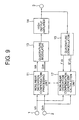
Fig. 9 is a block diagram showing the configuration of a
conventional system for compensating for nonlinear
distortions. As shown in Fig. 9, the system comprises a
nonlinear distortion compensation processing unit 11, a
quadrature modulator 13, a high output amplifier 14, a
quadrature demodulator 15, and a nonlinear distortion
compensation coefficient calculation unit 17. The apparatus
shown in Fig. 9 is intended for quadrature amplitude
modulation (QAM), and is applied a baseband quasi-synchronization
system which is a common digital
demodulation system. Further, in the explanation for the
operation of the apparatus shown in Fig. 9, typical
indications of Ich and Qch are used for in-phase and
quadrature components (channels), respectively.
Each element of the apparatus shown in Fig. 9 will be
described in detail below. The nonlinear distortion
compensation processing unit 11 has a function of performing
nonlinear distortion compensations to baseband signals for
Ich and Qch input into terminals 1 and 2, respectively, and
outputting them. The quadrature modulator 13 has a function
of quadrature-modulating baseband signals for Ich and Qch,
to which nonlinear distortion compensations have been
performed, and outputting the quadrature modulated signals.
The high output amplifier 14 has a function of amplifying
the quadrature modulated signals and outputting them as
modulated signals, which are output to the outside through a
terminal 3.
The quadrature demodulator 15 has a function of
outputting quadrature demodulated signals I'ch and Q'ch
generated by quadrature-demodulating the quadrature
modulated signals output from the high output amplifier 14.
The nonlinear distortion compensation coefficient
calculation unit 17, into which the baseband signals Ich and
Qch and the quadrature demodulated signals I'ch and Q'ch are
input, has a function of calculating and outputting a
nonlinear distortion compensation coefficient based on the
inverse characteristics of the nonlinear characteristics
corresponding to the amplitude of the baseband signals. The
nonlinear distortion compensation processing unit 11 has a
function of multiplying the baseband signals Ich and Qch by
data of the nonlinear distortion compensation coefficient,
and performing a predistortion (addition of the inverse
characteristics of the nonlinear distortion characteristics).
Here, brief explanations will be given for nonlinear
distortions caused in the
high output amplifier 14 with a
radio frequency (RF) band, and for an influence of the
linear distortions on transmitted signals. Note that the
characteristics of the
high output amplifier 14 are shown in
dB. It is defined that the input level of the high output
amplifier is Pi, the output level is Po, the amplification
gain is G, and the saturation power level is Psat. Assuming
that the
high output amplifier 14 has ideal characteristics,
a value, obtained by summing the input level Pi and the
amplification gain G, is output, unless the output level Po
is equal to or exceeds the saturation power level Psat.
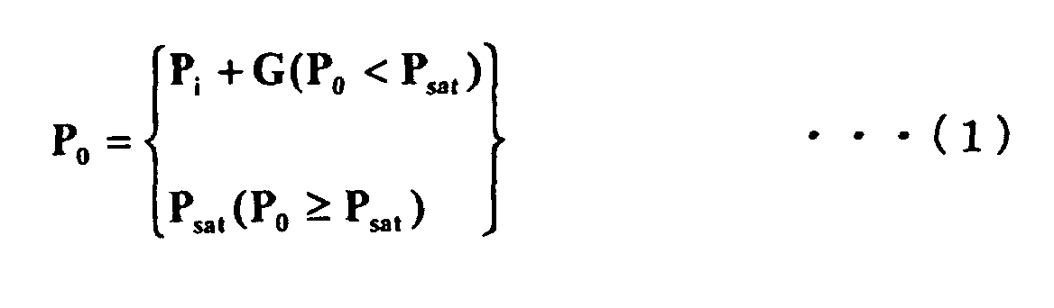
Thus, the input/output characteristics of the
high outuput
amplifier 14 is expressed as the following equation (1):
However, if the
high output amplifier 14 is configured
with practical electric circuits, the output level Po is
gradually compressed as the output level Po comes close to
the saturation power level Psat, whereby the characteristic
difference between the practical amplifier and an ideal
amplifier increases. According to a literature, Behavioral
Modeling of Nonlinear RF and Mocrowave Device, by Thomas r.
Turlington, Artech House, the input/output characteristics
of an amplifier, taking into account the compression effect,
can be approximated by the following equation (2).
Here, K is a positive number, which is an amplitude
compression coefficient showing the characteristics of the
amplifier. As K increases, the characteristics of the
amplifier degrade. In contrast, as K comes close to zero,
the characteristics of the amplifier becomes close to the
characteristics of an ideal amplifier.
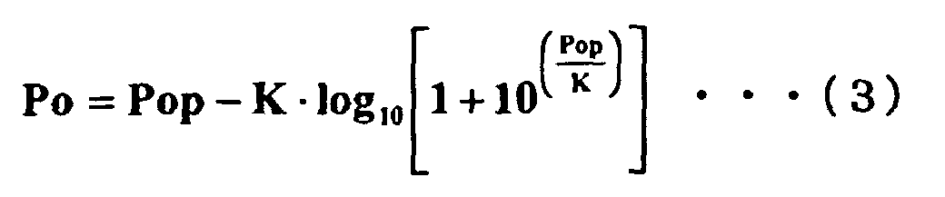
Further, with reference to the equation (2), if
defining that the saturation power level Psat is a reference
point (0dB), Pi+G is the operating point of the amplifier,
and the output level is Pop, respectively, the relationship
between the operating point and the output level of the
high
output amplifier 14 is shown as the following equation (3):
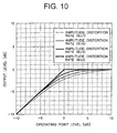
Fig. 10 shows characteristics against output of the
operating point of the amplifier, in a case that the
vertical axis shows the output level, K→0, and K=3, 5, 7.
Here, the horizontal axis shows the operating point of the
amplifier, and the vertical axis shows the output level. As
shown in Fig. 10, in the case of an ideal amplifier (K→0),
the operating point linearly operates until it comes to the
saturation power, and once it came to the saturation power,
the power is immediately clipped to the saturation point.
Further, the Figure shows that as the amplitude compression
coefficient K increases, the characteristic difference from
the ideal amplifier becomes large, causing the linear
operation to be less performed before the operating point
level exceeds the saturation point (0dB).
The modulated signals to be demodulated by the
demodulated apparatus, shown in Fig. 9, are quadrature
amplitude modulated (QAM) signals in which signal points
have plural amplitudes. Therefore, when the aforementioned
nonlinear operation occurs, there arises an influence of
nonlinear distortions with different compressibility on each
signal point, corresponding to the signal amplitude.
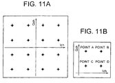
Fig. 11 shows an example of a signal point arrangement
of quadrature amplitude modulated signals to be demodulated
by the demodulator shown in Fig. 9. Fig. 11(a) shows a
normal signal point arrangement of QAM signals which are
sixteen quadrature amplitude modulated signals, and Fig.
11(b) shows a signal point arrangement, in which only a
first quadrant in the signal arrangement shown in Fig. 11(a)
is extracted. It should be noted that in Figs. 11(a) and
11(b), black circles show signal points, and + symbols show
normal positions of the signal points. Figs. 11(a) and
11(b) show the state where the black circles and + symbols
of the signal points overlap with each other.
As shown in Fig. 11(a), the normal signal point
arrangements of the sixteen quadrature amplitude modulated
signals exist on first to forth quadrants defined by the
horizontal axis Ich and the vertical axis Qch, with four
points having the same amplitude, respectively, in the same
manner. Hereinafter, the signal point arrangement will be
explained with respect to the first quadrant only, since the
amplitudes are same in the second to the forth quadrants and
the operations thereof are also similar. Further, the four
points in the signal point arrangement of the first quadrant
are named point A, point B, point C and point D,
respectively, for convenience.
Fig. 12 shows a signal point arrangement on the first
quadrant when the sixteen quadrature amplitude modulated
signals are affected by a nonlinear distortion. Here, the
black circles also represent signal points and the + symbols
also represent normal positions of the signal points. Fig.
12 shows a state where the black circles showing the signal
points are shifted from the + symbols showing the signal
points due to a nonlinear distortion.
As shown in Fig. 12, the outside signals (points A, B
and C) with larger amplitudes are more affected by the
nonlinear distortion, comparing with the inside signal
(point C) having a smaller amplitude, whereby the shifted
amounts of the outside signals from the normal signal point
positions indicated by the + symbols are large. In
particular, the signal point on the outermost side with the
largest amplitude, as the point B, is shifted significantly.
When demodulating such a signal, the margin between
the demodulated signal point and the judgment area is small,
whereby the outer side signal is more affected by noise, and
the error rate becomes worse. Note that the boundaries
shown by dashed lines in Fig. 12 are divisions of the signal
judgment areas.
When expressing the equation (3) by assigning a
variable x as the operating point power and a generalized
function F(x) as the output power, the following equation
(4) is established:
When using the inverse function of F(x), the following
equation (5), in which the input is the output power and the
output is the operation point power, inversely, can be
established:
Pop = F-1 (Po)
It is difficult to express the inverse function, used
in the equation (5), as a formula. However, since Pop and
Po in the equation (4) have a relationship of one to one,
the relationship in the equation (5) can be expressed in Fig.
13, using a numerical calculation by assigning a parameter K.
In Fig. 13, nonlinear distortions caused in the RF amplifier
are expressed as the characteristics of the operating point
level (dB) with reference to the output level (dB). The
output level shown by the horizontal axis corresponds to the
input power into the nonlinear distortion compensation
processing unit 11, and the operation point level shown by
the vertical axis corresponds to the output level after the
predistortion is performed.
Further, when defining the amplitude ratio of the
output power to the operating point power as the amplitude
compensation rate Re, and the amplitude of the output power
as the input amplitude of the quadrature demodulator 15, the
amplitude compensation rate characteristics of the
quadrature demodulator 15 to the input amplitude can be
expressed as shown in Fig. 14.
In Fig. 14, the horizontal axis shows the ratio to the
amplitude of the saturation power in dB. Thereby, if the
operating points of the output signals of the high output
amplifier can be estimated, the amplitude compensation rate
can be calculated by converting the input amplitude of the
nonlinear distortion compensation processing unit 11 into dB.
Hereinafter, the operating point of the average signal power
is defined as the average operating point. An influence of
the amplitude distortions can be compensated by tracking the
average operating point corresponding to the adaptive
operation, calculating the amplitude compensation rate
according to the operating point of the average signal power
detected and the input amplitude of the nonlinear distortion
compensation processing unit 11, and multiplying the input
signals by the amplitude compensation rate.
Fig. 15 is a block diagram showing the configuration
of the nonlinear distortion compensation coefficient
calculation unit 17. As shown in Fig. 15, the nonlinear
distortion compensation coefficient calculation unit 17
comprises: a root-sum-square calculation circuit 23, an
amplitude compensation rate calculation table processing
circuit 24, an average operating point estimation circuit 25,
a compensation polarity detection circuit 26, a judgment
circuit 27, terminals 56 to 59, and a terminal 60. To the
terminals 56 and 57, baseband signals Ich and Qch are input,
respectively. The root-sum-square calculation circuit 23
outputs signals, which are resultants of calculating root
sum square of the amplitude of the respective baseband
signals Ich and Qch, as an input amplitude to the amplitude
compensation rate calculation table processing circuit 24.
To the terminals 58 and 59, quadrature demodulated
signals Ich' and Qch' are input, respectively. The judgment
circuit 27 judges a transmitted symbol based on the
quadrature demodulated signals Ich' and Qch', and generates
and outputs data signals and error signals. The
compensation polarity detection circuit 26, corresponding to
the result of judging the appropriateness of the amplitude
distortion compensation based on the compensation polarity
area defined by the boundary where the vector of the input
error signal becomes perpendicular to the vector of the data
signal, generates a control signal for adjusting the
compensation amount in the amplitude distortion compensation,
and output it to the average operating point estimation
circuit 25.
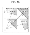
Fig. 16 is a chart showing an example of a
compensation polarity detection area for detecting an
influence of distortion from a signal point arrangement.
The compensation polarity detection circuit 26 estimates an
area where data exist according to the data signals output
from the judgment circuit 27, and detects an influence of
distortions based on judgment reference data which vary
according to the area where the signals exist, and on the
error signals. More specifically, in the compensation
polarity detection circuit 26, the origin 0 of the signal
point arrangement and the normal signal point position are
linked by a straight line, and a straight line perpendicular
to the straight line is set as a boundary, and by judging
the inside of the boundary (origin 0 side, no shading) as an
area affecting the positive nonlinear distortion, and by
judging the outside of the boundary (shaded parts) as an
area affecting the negative nonlinear distortion, an
adaptive operation is performed so that the both judged
areas are generated with the equal possibility.
The average operating point estimation circuit 25
generates and outputs an average operation point estimation
value by adaptively changing it, corresponding to the
control signal output from the compensation polarity
detection circuit 26. The amplitude compensation rate
calculation table processing circuit 24 has an amplitude
compensation rate calculation table, with which an amplitude
compensation rate can be delivered by assigning an average
operating point estimated value output from the average
operating point estimation circuit 25 and an input amplitude
output from the root-sum-square calculation circuit 23. The
amplitude compensation rate calculation table processing
circuit 24 outputs data of amplitude compensation rate,
delivered from the table, which data is output to the
outside through the terminal 60.
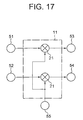
Fig. 17 is a block diagram showing the configuration
of the nonlinear distortion compensation processing unit 11.
As shown in Fig. 17, the nonlinear distortion compensation
processing unit 11 comprises terminal 51 to 55, and two
multipliers 21. To the terminals 51 and 52, baseband
signals Ich and Qch from the terminals 1 and 2 are input,
respectively. To the terminal 55, an amplitude compensation
rate signal is input. Respective multipliers 21 multiply
the input baseband signals Ich and Qch by the amplitude
compensation rate signal, respectively, and output the
resultant signals. The resultant signals output from the
multipliers 21 are output through the terminals 53 and 54,
respectively.
However, the nonlinear distortion compensation
operation described above uses the result obtained by a
numerical calculation based on the expected characteristics
of the high output amplifier 14. Thereby, there has been a
problem that expected nonlinear distortion compensation
characteristics may not be exhibited when the operation is
affected by incompleteness of the amplitude delay
characteristics or an intrinsic deviation, that the
quadrature modulator 13 or the high output amplifier 14 have.
In other words, since a conventional demodulator
performs only nonlinear compensations on the transmitter
side, linear distortions caused by the incompleteness of the
amplitude delay characteristics or intrinsic deviation of an
analog circuit are not reduced. Thereby, there has been a
problem that an effect of the nonlinear distortion
compensation characteristics may not be fully exhibited due
to the influence of the linear distortions.
It is therefore an object of the invention to provide
a transmitter, capable of performing an ideal nonlinear
distortion compensation, in which an influence of
incompleteness of the amplitude delay characteristics or an
intrinsic deviation, that an amplifier has, is eliminated.
Disclosure of the Invention
In order to solve the aforementioned problems, a
transmission method according to the present invention is
for compensating for nonlinear distortions caused by
amplifying modulated signals obtained by modulating baseband
signals to have a radio frequency band, which comprises the
step of compensating for, in addition to the nonlinear
distortions, linear distortions by adding inverse
characteristics of linear distortion characteristics that
amplified modulated signals have. Note that linear
distortions may be compensated before nonlinear distortions
are compensated, or nonlinear distortions may be compensated
before linear distortions are compensated.
As described above, in the transmission method of the
present invention, linear distortions are compensated by
adding inverse characteristics of the linear distortion
characteristics that the amplified modulated signals have,
in addition to the nonlinear distortions caused by
amplifying modulated signals being compensated.
Therefore, according to the present invention, an
influence of incompleteness of amplitude delay
characteristics or an intrinsic deviation that an analog
circuit has can be eliminated by compensating for linear
distortions, whereby it is possible to enhance the accuracy
of predistortion for compensating for nonlinear distortions
in a high output amplifier, and to perform an ideal
nonlinear distortion compensation.
Further, a transmitter for carrying out the
transmission method of the present invention is one in which
nonlinear distortions are compensated, the nonlinear
distortions being caused by amplifying modulated signals
obtained by modulating baseband signals to have a radio
frequency signal. The transmitter comprises: a quadrature
demodulator which outputs quadrature demodulated signals
obtained by demodulating the modulated signals; a linear
distortion compensation coefficient calculation unit for
calculating and outputting a linear distortion compensation
coefficient for compensating for linear distortions
contained in the quadrature demodulated signals; and a
linear distortion compensation processing unit for
multiplying the baseband signals by data of the linear
distortion compensation coefficient and outputting resultant
signals.
Therefore, according to the present invention, an
influence of incompleteness of amplitude delay
characteristics or an intrinsic deviation that an analog
circuit has can be eliminated by compensating for linear
distortions, whereby it is possible to enhance the accuracy
of predistortion for compensating for nonlinear distortions
in a high output amplifier, and to perform an ideal
nonlinear distortion compensation.
Brief Description of Drawings
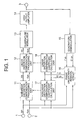
Fig. 1 is a block diagram showing the configuration of
a transmitter according to a first embodiment of the present
invention. Fig. 2 is a block diagram showing an exemplary
configuration of the phase uncertainty removal circuit. Fig.
3 is a block diagram showing an exemplary configuration of
the linear distortion compensation coefficient calculation
unit. Fig. 4 is a block diagram showing an exemplary
configuration of the linear distortion compensation
coefficient calculation circuit. Fig. 5 is a block diagram
showing an exemplary configuration of the linear distortion
compensation processing unit. Fig. 6 is a block diagram
showing an exemplary configuration of a transversal filter.
Fig. 7 is a block diagram showing an exemplary configuration
of a case where a phase uncertainty removal circuit is
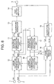
excluded. Fig. 8 is a block diagram showing a deformed
example of the configuration of the transmitter. Fig. 9 is
a block diagram showing a conventional system configuration
for compensating for nonlinear distortions. Fig. 10 is a
graph showing characteristics against output of an operating
point of the amplifier. Fig. 11 is a chart showing an
signal point arrangement of QAM signals to be demodulated by
the demodulator of the present embodiment. Fig. 12 is a
chart showing an signal point arrangement on a first
quadrant being affected by nonlinear distortions of 16QAM
signals. Fig. 13 is a graph showing the characteristics of
the operating point level with reference to the output level.
Fig. 14 is a graph showing the amplitude compensation ratio
of the quadrature demodulator to the input amplitude. Fig.
15 is a block diagram showing the configuration of the
nonlinear distortion compensation coefficient calculation
unit. Fig. 16 is a chart showing an example of a
compensation polarity detection area for detecting an
influence of distortions from a signal point arrangement.
Fig. 17 is a block diagram showing the configuration of the
nonlinear distortion compensation processing unit.
Best Mode for Carrying Out the Invention
A transmitter according to an embodiment of the
present invention will be described in detail below with
reference to the drawings. Fig. 1 is a block diagram
showing the constitution of a transmitter according to the
present embodiment. As shown in Fig. 1, a transmission
method of the present invention is for compensating for
nonlinear distortions caused by amplifying modulated signals
obtained by modulating baseband signals to have a radio
frequency band. In the method, in addition to the nonlinear
distortions, linear distortions are also compensated by
adding inverse characteristics of linear distortion
characteristics that the amplified, modulated signals have.
A transmitter for performing such a transmission method
includes, in addition to the configuration shown in Fig. 9,
a linear distortion compensation processing unit 12, a phase
uncertainty removal circuit 16, and a linear distortion
compensation coefficient calculation unit 18. It should be
noted that linear distortions may be compensated before
nonlinear distortions are compensated, or nonlinear
distortions may be compensated before linear distortions are
compensated.
The transmitter of the present invention compensates
for nonlinear distortions generated in the high output
amplifier 14 with an RF band, in the nonlinear distortion
compensation processing unit 11, and is further provided
with a function of compensating for incompleteness of
amplitude delay characteristics or an intrinsic deviation
that the quadrature modulator 13 or the high output
amplifier 14 have, in order that the effect of the nonlinear
distortion compensation can be fully exhibited.
Next, the transmitter of the present embodiment will
be described more specifically. The linear distortion
compensation coefficient calculation unit 18 has a function
of estimating linear distortion characteristics caused by
incompleteness of an analog circuit mainly such as the
quadrature modulator 13 or the high output amplifier 14,
based on quadrature demodulated signals I'ch and Q'ch output
from the phase uncertainly removal circuit 16, and
calculating and outputting a linear distortion compensation
coefficient for compensating for linear distortions. The
linear distortion compensation processing unit 12 has a
function of performing a predistortion (addition of inverse
characteristics of linear distortion characteristics) by
adding data of the linear distortion compensation
coefficient, output from the linear distortion compensation
coefficient calculation unit 18, to the baseband signals Ich
and Qch output from the nonlinear compensation processing
unit 11.
The nonlinear distortion compensation coefficient
calculation unit 17 shown in Fig. 1 has a function of
estimating nonlinear distortion characteristics caused by
incompleteness of an analog circuit mainly such as the
quadrature modulator 13 or the high output amplifier 14,
based on quadrature demodulated signals I'ch and Q'ch output
from the phase uncertainly removal circuit 16, and
calculating and outputting a nonlinear distortion
compensation coefficient for compensating for nonlinear
distortions. The nonlinear distortion compensation
processing unit 11 has a function of performing a
predistortion (addition of inverse characteristics of linear
distortion characteristics) by adding data of the nonlinear
distortion compensation coefficient, output from the
nonlinear distortion compensation coefficient calculation
unit 17, to the baseband signals Ich and Qch output from the
terminals 1 and 2.
Therefore, when the quadrature demodulated signal I'ch
and Q'ch output from the phase uncertainty removal circuit
16 are input into the linear distortion compensation
coefficient calculation unit 18, the linear distortion
compensation coefficient calculation unit 18 estimates
linear distortion characteristics caused by incompleteness
of an analog circuit mainly such as the quadrature modulator
13 or the high output amplifier 14 based on the quadrature
demodulated signals I'ch and Q'ch, calculates a linear
distortion compensation coefficient for compensating for the
linear distortions, and outputs the data to the linear
distortion compensation processing unit 12. Then, when the
data of the linear distortion compensation coefficient
output from the linear distortion compensation coefficient
calculation unit 18 is input into the linear distortion
compensation processing unit 12, the linear distortion
compensation processing unit 12 performs predistortion
(addition of inverse characteristics of linear distortion
characteristics) by adding the data of the linear distortion
compensation coefficient to the baseband signals Ich and Qch
output from the nonlinear distortion compensation processing
unit 11.
When the quadrature demodulated signals I'ch and Q'ch
are output from the phase uncertainty removal circuit 16 are
input into the nonlinear distortion compensation coefficient
calculation unit 17, the nonlinear distortion compensation
coefficient calculation unit 17 estimates the nonlinear
distortion characteristics caused by incompleteness of an
analog circuit mainly such as the quadrature modulator 13 or
the high output amplifier 14 based on the quadrature
demodulated signals I'ch and Q'ch, calculates an nonlinear
distortion compensation coefficient for compensating for the
nonlinear distortion, and output the data to the nonlinear
distortion compensation processing unit 11. Then, when the
data of the nonlinear distortion compensation coefficient
output from the nonlinear distortion compensation
coefficient calculation unit 17 is input into the nonlinear
distortion compensation processing unit 11, the nonlinear
distortion compensation processing unit 11 performs
predistortion (addition of inverse characteristics of linear
distortion characteristics) by adding the data of the
nonlinear distortion compensation coefficient to the
baseband signals Ich and Qch output from the terminals 1 and
2.
As described above, in addition to a compensation of
nonlinear distortions caused by amplifying modulated signals
obtained by modulating the baseband signals to have a radio
frequency (RF) band, a linear distortion compensation is
performed by adding inverse characteristics of linear
distortion characteristics that the amplified, modulated
signals have (that is, predistortion). Therefore, in the
transmitter of the present embodiment, respective
transmitted symbols input from the terminals 1 and 2 are
performed predistortion in the nonlinear distortion
compensation processing unit 11 and the linear distortion
compensation processing unit 12, respectively, and are
modulated into RF signals by the quadrature modulator 13,
are amplified by the high output amplifier 14, and are
output from the terminal 3.
Note that in the transmitter of the present embodiment,
the baseband signals (quadrature demodulated signals) I'ch
and Q'ch are independently (that is, in the state of two
dimension) input for feedback so as to operate the nonlinear
distortion compensation calculation unit 17 and the linear
distortion compensation coefficient calculation unit 18,
whereby phase uncertainties of the quadrature-modulated
feedback signals are removed in the phase uncertainty
removal circuit 16
Fig. 2 is a block diagram showing an exemplary
constitution of the phase uncertainty removal circuit 16
shown in Fig. 1. As shown in Fig. 2, the phase uncertainty
removal circuit 16 has a function of removing phase
uncertainties of the quadrature demodulated signals I'ch and
Q'ch output from the quadrature demodulator 15. The phase
uncertainty removal circuit 16 comprises: a delay adjustment
circuit 40 for adjusting a timing of the transmitted symbols
input from terminals 77 and 78 connected with the terminals
1 and 2, and the quadrature signals I'ch and Q'ch from the
quadrature demodulator 15; a comparator 41 for comparing the
transmitted symbols input from the terminals 77 and 78 with
the quadrature demodulated signals I'ch and Q'ch from the
quadrature demodulator 15, and determining the phase
difference thereof; and a selection circuit 39 for selecting
an output from a phase rotation adding circuit 42 to 45
corresponding to the result determined by the comparator 41,
and outputting the quadrature demodulated signals I'ch and
Q'ch in which phase uncertainties are removed. To the
terminals 75 and 76 of the phase uncertainty removal circuit
16, the quadrature demodulated signals I'ch and Q'ch from
the quadrature demodulator 15 are input, and to the
terminals 77 and 78, the transmitted symbols from the
terminals 1 and 2 are input. Further, the quadrature
demodulator 15 is so configured as to output the quadrature
demodulated signals I'ch and Q'ch obtained by demodulating
the modulated signal amplified by the high output amplifier
14.
When the transmitted symbols are input into the delay
adjustment circuit 40 of the phase uncertainty removal
circuit 16 through the terminals 77 and 78, the delay
adjustment circuit 40 performs delay adjustments of timings
of the transmission symbols and the quadrature demodulated
signals, and outputs the signals to the comparator 41. When
the delay adjusted signals and the quadrature demodulated
signals I'ch and Q'ch from the terminals 75 and 76 are input
into the comparator 41, the comparator 41 compares the
signals delay-adjusted in the delay adjustment circuit 40
with the quadrature demodulated signals I'ch and Q'ch so
that the timing of the quadrature demodulated signals I'ch
and Q'ch and the transmitted symbols coincide with each
other, and then determines whether the phase difference
between the both signals is 0, π/2, π or 3π/2. When the
signal, which is the comparison result from the comparator
41, is input into the selection circuit 39, the selection
circuit 39 selects one output (0, π/2, π, 3π/2) from the
phase rotation adding circuit 42, 43, 44 or 45,
corresponding to the result determined in the comparator 41,
whereby removes phase uncertainties in the quadrature
demodulated signals I'ch and Q'ch, and outputs the
quadrature demodulated signals I'ch and Q'ch in which the
phase uncertainties are removed. The output of the
selection circuit 39 is output to the nonlinear distortion
coefficient calculation unit 17 and to the linear distortion
compensation coefficient calculation unit 18 through the
terminals 79 and 80.
Fig. 3 is a block diagram showing an exemplary
configuration of the linear distortion compensation
coefficient calculation unit 18 shown in Fig. 1. As shown
in Fig. 3, the linear distortion compensation coefficient
calculation unit 18 has a function of calculating and
outputting a linear distortion compensation coefficient for
compensating for linear distortions included in the
quadrature demodulated signals I'ch and Q'ch from the phase
uncertainty removal circuit 16, and comprises, terminals 66
to 68, two judgment circuits 34, and linear distortion
compensation coefficient calculation circuits 35 of four
systems, that is, Ich in-phase, Ich quadrature, Qch in-phase,
and Qch quadrature.
To the terminals 66 and 67, quadrature demodulated
signals I'ch and Q'ch output from the phase uncertainty
removal circuit 16 ( terminals 79 and 80 in Fig. 2) are input,
respectively. Two judgment circuits 34 have a function of
judging transmitted symbols according to the quadrature
demodulated signals input from the terminal 66 and 67, and
reproducing and outputting data signals (reproduction of
transmitted signals) ID and QD, and error signals IE and QE,
of respective channels.
Here, the data signal ID from the judgment circuit 34
is input into the linear distortion compensation coefficient
circuits 35 of Ich in-phase and Qch quadrature, respectively,
and the error signal IE is input into the linear distortion
compensation coefficient calculation circuits 35 of Ich in-phase
and Ich quadrature, respectively. Further, the data
signal QD from the judgment circuit 34 is input into the
linear distortion compensation coefficient calculation
circuits 35 of Qch in-phase and Ich quadrature, respectively,
and the error signal QE is input into the linear distortion
compensation calculation circuits 35 of Qch in-phase and Qch
quadrature, respectively.
Therefore, when the quadrature demodulated signals
I'ch and Q'ch from the phase uncertainty removal circuit 16
are input into the judgment circuits 34 through the
terminals 66 and 67, the two judgment circuits 34 reproduce
data signals (reproduction of transmitted signals) ID and QD
and error signals IE and QE respectively, for each of the
quadrature demodulated signals I'ch and Q'ch, and output
them to the linear distortion compensation coefficient
calculation circuits 35 of four systems, that is, Ich in-phase,
Ich quadrature, Qch in-phase, and Qch quadrature.
Then, respective linear distortion compensation coefficient
circuits 35 calculate linear distortion compensation
coefficients of in-phase and quadrature for respective
channels, based on the data signals ID and QD and the error
signals IE and QE, respectively, by using, as inputs, the
linear distortion compensation coefficient for compensating
linear distortions included in the quadrature demodulated
signals I'ch and Q'ch, that is, data signals ID and QD and
the error signals IE and QE of respective channels, and the
linear distortion compensation coefficient circuits 35
output data of the linear distortion compensation
coefficients (CII, CQI, CIQ, CQQ), which are the calculation
results, from the terminal 68. In Fig. 3, lines to the
terminal 68 of respective linear distortion compensation
coefficient calculation circuits 35 are indicated with the
"numeral 3, and a slash /", indicating that each linear
distortion compensation coefficient circuit 35 outputs tap
coefficients (C+1, C0, C-1) as linear distortion
compensation coefficients from three terminals (terminals 74
in Fig. 4).
Fig. 4 is a block diagram showing an exemplary
configuration of each linear distortion compensation
coefficient calculation circuit 35 shown in Fig. 3. As
shown in Fig. 4, the linear distortion compensation
coefficient circuit 35 comprises: terminals 72 and 73 to
which the data signals (ID, QD) and the error signals (IE,
QE) from the judgment circuits 34 are input, three delay
elements 36, three correlators 37, three integrators 38, and
a terminal 74 from which data of tap coefficients (C+1, C0,
C-1) from the integrators are output. The linear distortion
compensation coefficient calculation circuit 35 shown in Fig.
4 is a tap coefficient calculation circuit of three-tap
transversal filter, and the calculation of the tap
coefficients (C+1, C0, C-1) performed in the linear
distortion compensation coefficient calculation circuit 35
is same as the operation of a well-known linear equalizer,
whereby the detail explanations are omitted.
Fig. 5 is a block diagram showing an exemplary
configuration of the linear distortion compensation
processing unit 12 shown in Fig. 1. As shown in Fig. 5, the
linear distortion compensation processing unit 12 has a
function of multiplying the baseband signals (Ich, Qch) from
the nonlinear distortion compensation processing unit 11 by
data of linear distortion compensation coefficient from the
linear distortion compensation coefficient calculation unit
18, and outputting the resultant signals, and comprises:
terminals 61 and 62 into which baseband signals from the
nonlinear distortion compensation processing unit 11 are
input, four transversal filters 29, and two adders 30.
The four transversal filters 29 are four system
transversal filters of Ich in-phase, Ich quadrature, Qch in-phase,
and Qch quadrature, respectively. The baseband
signal Ich input into the terminal 61 is input into the Ich
in-phase transversal filter 29 and the Qch quadrature
transversal filter 29, respectively, and the baseband signal
Qch is input into the Qch in-phase transversal filter 29 and
the Ich quadrature transversal filter 29, respectively.
Further, the four-system transversal filters 29 of Ich
in-phase, Ich quadrature, Qch in-phase and Qch quadrature,
performs linear distortion compensation based on the
coefficients (CII, CQI, CIQ, CQQ) input from the linear
distortion compensation coefficient calculation unit 18
through the terminal 65. Each piece of data of the linear
distortion compensation coefficients (CII, CQI, CIQ, CQQ)
includes data of three tap coefficients (C+1, C, C-1),
respectively.
Further, one adder 30 adds an in-phase component from
the Ich in-phase transversal filter 29 and a quadrature
component from the Ich quadrature transversal filter 29 and
outputs the resultant, and the other adder 30 adds an in-phase
component from the Qch in-phase transversal filter 29
and a quadrature component from the Qch quadrature
transversal filter 29 and outputs the resultant. Further,
the output signals from respective adders 30 are output
through the terminals 63 and 64 to the quadrature modulator
13.
Thus, when the baseband signals Ich and Qch from the
nonlinear distortion compensation processing unit 11 are
input into the terminals 61 and 62, these baseband signals
Ich and Qch are input into the four transversal filters 29,
as described above. Then, the four-system transversal
filters 29 of Ich in-phase, Ich quadrature, Qch in-phase and
Qch quadrature perform linear distortion compensation based
on the data of linear distortion compensation coefficients
(CII, CQI, CIQ, CQQ), which are input from the linear
distortion compensation coefficient calculation unit 18
through the terminal 65. One adder 30 adds an in-phase
component and a quadrature component of the Ich transversal
filter 29 and outputs the resultant, and the other adder 30
adds an in-phase component and a quadrature component of the
Qch transversal filter 29 and outputs the resultant. The
outputs of respective adders 30 are output to the outside
through the terminals 63 and 64.
Fig. 6 is a block diagram showing an exemplary
configuration of a transversal filter 29 shown in Fig. 5.
As shown in Fig. 6, the transversal filter 29 is a
transversal filter operable at a clock rate, and is
configured as a three-tap linear equalizer comprising two
delay elements 31, three multipliers 32, and one adder 33.
To the multipliers 32, the tap coefficients, C+1, C0
and C-1, output from the linear distortion compensation
coefficient calculation circuit 35 are input through the
terminal 71, in which signals from the terminal 69 are
directly input into a first multiplier 32, signals passing
through one delay element 31 are input into a second
multiplier 32, and signals passing through two delay
elements 31 are input into a third multiplier 32. Then,
signals from three multipliers 32 are input into the adder
33, and signals from the adder 33 are output to the adder 30
shown in Fig. 5 through the terminal 70.
The number of taps of the transversal filter 29 are
not limited, and instead of the transversal filter operable
at a clock rate shown in Fig. 6, a fractional-type
transversal filter operable at a multiplication of the clock
rate may be applied. Each tap coefficient of the
transversal filter is calculated and supplied by the linear
distortion compensation calculation unit 18. It should be
noted that the operation of the transversal filter 29 is
same as that of a well-known linear equalizer, whereby the
detail explanations are omitted.
As described above, the transmitter of the present
invention compensates for nonlinear distortions caused by
amplifying modulated signals, and also compensates for
linear distortions. Thereby, an influence of incompleteness
of amplitude delay characteristics or an intrinsic deviation
that an analog circuit has, is eliminated by performing the
linear distortion compensation, so that an ideal nonlinear
distortion compensation can be carried out.
In the transmitter of the present invention, phase
decision is performed by the phase uncertainty removal
circuit 16 in order to enhance the accuracy of the
predistortion. However, linear distortion compensation and
nonlinear distortion compensation may be performed without
carrying out the phase decision by the phase uncertainty
removal circuit 16. Fig. 7 shows the configuration of the
transmitter where the phase uncertainty removal circuit is
excluded.
Further, in the transmitter of the present invention,
the nonlinear distortion compensation processing unit 11 is
provided in the preceding stage to the linear distortion
compensation processing unit 12, and the linear distortion
compensation is performed first, followed by the nonlinear
distortion compensation. However, the linear distortion
compensation processing unit 12 may be provided in the
preceding stage to the nonlinear distortion compensation
processing unit 11, whereby the linear distortion
compensation may be performed first, followed by the
nonlinear distortion compensation. Fig. 8 shows the
configuration of the transmitter in such a case.
Industrial Applicability
As described above, the present invention performs
predistortion for compensating for linear distortions, in
addition to nonlinear distortions caused by incompleteness
of an analog circuit, whereby it is possible to enhance the
accuracy of the predistortion for compensating for linear
distortions of a high output amplifier, and to perform an
ideal nonlinear distortion compensation.