EP1482374A2 - Méthode de génération de données de distorsion d'un masque, méthode d'exposition et méthode de fabrication d'un dispositif semiconducteur - Google Patents
Méthode de génération de données de distorsion d'un masque, méthode d'exposition et méthode de fabrication d'un dispositif semiconducteur Download PDFInfo
- Publication number
- EP1482374A2 EP1482374A2 EP04012335A EP04012335A EP1482374A2 EP 1482374 A2 EP1482374 A2 EP 1482374A2 EP 04012335 A EP04012335 A EP 04012335A EP 04012335 A EP04012335 A EP 04012335A EP 1482374 A2 EP1482374 A2 EP 1482374A2
- Authority
- EP
- European Patent Office
- Prior art keywords
- mask
- positional accuracy
- accuracy measurement
- thin film
- measurement marks
- Prior art date
- Legal status (The legal status is an assumption and is not a legal conclusion. Google has not performed a legal analysis and makes no representation as to the accuracy of the status listed.)
- Withdrawn
Links
Images


Classifications
-
- G—PHYSICS
- G03—PHOTOGRAPHY; CINEMATOGRAPHY; ANALOGOUS TECHNIQUES USING WAVES OTHER THAN OPTICAL WAVES; ELECTROGRAPHY; HOLOGRAPHY
- G03F—PHOTOMECHANICAL PRODUCTION OF TEXTURED OR PATTERNED SURFACES, e.g. FOR PRINTING, FOR PROCESSING OF SEMICONDUCTOR DEVICES; MATERIALS THEREFOR; ORIGINALS THEREFOR; APPARATUS SPECIALLY ADAPTED THEREFOR
- G03F9/00—Registration or positioning of originals, masks, frames, photographic sheets or textured or patterned surfaces, e.g. automatically
- G03F9/70—Registration or positioning of originals, masks, frames, photographic sheets or textured or patterned surfaces, e.g. automatically for microlithography
- G03F9/7003—Alignment type or strategy, e.g. leveling, global alignment
-
- G—PHYSICS
- G03—PHOTOGRAPHY; CINEMATOGRAPHY; ANALOGOUS TECHNIQUES USING WAVES OTHER THAN OPTICAL WAVES; ELECTROGRAPHY; HOLOGRAPHY
- G03F—PHOTOMECHANICAL PRODUCTION OF TEXTURED OR PATTERNED SURFACES, e.g. FOR PRINTING, FOR PROCESSING OF SEMICONDUCTOR DEVICES; MATERIALS THEREFOR; ORIGINALS THEREFOR; APPARATUS SPECIALLY ADAPTED THEREFOR
- G03F1/00—Originals for photomechanical production of textured or patterned surfaces, e.g., masks, photo-masks, reticles; Mask blanks or pellicles therefor; Containers specially adapted therefor; Preparation thereof
- G03F1/20—Masks or mask blanks for imaging by charged particle beam [CPB] radiation, e.g. by electron beam; Preparation thereof
-
- G—PHYSICS
- G03—PHOTOGRAPHY; CINEMATOGRAPHY; ANALOGOUS TECHNIQUES USING WAVES OTHER THAN OPTICAL WAVES; ELECTROGRAPHY; HOLOGRAPHY
- G03F—PHOTOMECHANICAL PRODUCTION OF TEXTURED OR PATTERNED SURFACES, e.g. FOR PRINTING, FOR PROCESSING OF SEMICONDUCTOR DEVICES; MATERIALS THEREFOR; ORIGINALS THEREFOR; APPARATUS SPECIALLY ADAPTED THEREFOR
- G03F1/00—Originals for photomechanical production of textured or patterned surfaces, e.g., masks, photo-masks, reticles; Mask blanks or pellicles therefor; Containers specially adapted therefor; Preparation thereof
- G03F1/38—Masks having auxiliary features, e.g. special coatings or marks for alignment or testing; Preparation thereof
- G03F1/42—Alignment or registration features, e.g. alignment marks on the mask substrates
-
- G—PHYSICS
- G03—PHOTOGRAPHY; CINEMATOGRAPHY; ANALOGOUS TECHNIQUES USING WAVES OTHER THAN OPTICAL WAVES; ELECTROGRAPHY; HOLOGRAPHY
- G03F—PHOTOMECHANICAL PRODUCTION OF TEXTURED OR PATTERNED SURFACES, e.g. FOR PRINTING, FOR PROCESSING OF SEMICONDUCTOR DEVICES; MATERIALS THEREFOR; ORIGINALS THEREFOR; APPARATUS SPECIALLY ADAPTED THEREFOR
- G03F1/00—Originals for photomechanical production of textured or patterned surfaces, e.g., masks, photo-masks, reticles; Mask blanks or pellicles therefor; Containers specially adapted therefor; Preparation thereof
- G03F1/68—Preparation processes not covered by groups G03F1/20 - G03F1/50
-
- G—PHYSICS
- G03—PHOTOGRAPHY; CINEMATOGRAPHY; ANALOGOUS TECHNIQUES USING WAVES OTHER THAN OPTICAL WAVES; ELECTROGRAPHY; HOLOGRAPHY
- G03F—PHOTOMECHANICAL PRODUCTION OF TEXTURED OR PATTERNED SURFACES, e.g. FOR PRINTING, FOR PROCESSING OF SEMICONDUCTOR DEVICES; MATERIALS THEREFOR; ORIGINALS THEREFOR; APPARATUS SPECIALLY ADAPTED THEREFOR
- G03F7/00—Photomechanical, e.g. photolithographic, production of textured or patterned surfaces, e.g. printing surfaces; Materials therefor, e.g. comprising photoresists; Apparatus specially adapted therefor
- G03F7/20—Exposure; Apparatus therefor
- G03F7/2045—Exposure; Apparatus therefor using originals with apertures, e.g. stencil exposure masks
-
- G—PHYSICS
- G03—PHOTOGRAPHY; CINEMATOGRAPHY; ANALOGOUS TECHNIQUES USING WAVES OTHER THAN OPTICAL WAVES; ELECTROGRAPHY; HOLOGRAPHY
- G03F—PHOTOMECHANICAL PRODUCTION OF TEXTURED OR PATTERNED SURFACES, e.g. FOR PRINTING, FOR PROCESSING OF SEMICONDUCTOR DEVICES; MATERIALS THEREFOR; ORIGINALS THEREFOR; APPARATUS SPECIALLY ADAPTED THEREFOR
- G03F9/00—Registration or positioning of originals, masks, frames, photographic sheets or textured or patterned surfaces, e.g. automatically
- G03F9/70—Registration or positioning of originals, masks, frames, photographic sheets or textured or patterned surfaces, e.g. automatically for microlithography
- G03F9/7073—Alignment marks and their environment
- G03F9/7084—Position of mark on substrate, i.e. position in (x, y, z) of mark, e.g. buried or resist covered mark, mark on rearside, at the substrate edge, in the circuit area, latent image mark, marks in plural levels
-
- H—ELECTRICITY
- H01—ELECTRIC ELEMENTS
- H01J—ELECTRIC DISCHARGE TUBES OR DISCHARGE LAMPS
- H01J37/00—Discharge tubes with provision for introducing objects or material to be exposed to the discharge, e.g. for the purpose of examination or processing thereof
- H01J37/30—Electron-beam or ion-beam tubes for localised treatment of objects
- H01J37/317—Electron-beam or ion-beam tubes for localised treatment of objects for changing properties of the objects or for applying thin layers thereon, e.g. for ion implantation
- H01J37/3174—Particle-beam lithography, e.g. electron beam lithography
-
- H—ELECTRICITY
- H01—ELECTRIC ELEMENTS
- H01J—ELECTRIC DISCHARGE TUBES OR DISCHARGE LAMPS
- H01J2237/00—Discharge tubes exposing object to beam, e.g. for analysis treatment, etching, imaging
- H01J2237/30—Electron or ion beam tubes for processing objects
- H01J2237/304—Controlling tubes
- H01J2237/30455—Correction during exposure
- H01J2237/30461—Correction during exposure pre-calculated
-
- H—ELECTRICITY
- H01—ELECTRIC ELEMENTS
- H01J—ELECTRIC DISCHARGE TUBES OR DISCHARGE LAMPS
- H01J2237/00—Discharge tubes exposing object to beam, e.g. for analysis treatment, etching, imaging
- H01J2237/30—Electron or ion beam tubes for processing objects
- H01J2237/317—Processing objects on a microscale
- H01J2237/3175—Lithography
- H01J2237/31793—Problems associated with lithography
- H01J2237/31794—Problems associated with lithography affecting masks
-
- Y—GENERAL TAGGING OF NEW TECHNOLOGICAL DEVELOPMENTS; GENERAL TAGGING OF CROSS-SECTIONAL TECHNOLOGIES SPANNING OVER SEVERAL SECTIONS OF THE IPC; TECHNICAL SUBJECTS COVERED BY FORMER USPC CROSS-REFERENCE ART COLLECTIONS [XRACs] AND DIGESTS
- Y10—TECHNICAL SUBJECTS COVERED BY FORMER USPC
- Y10S—TECHNICAL SUBJECTS COVERED BY FORMER USPC CROSS-REFERENCE ART COLLECTIONS [XRACs] AND DIGESTS
- Y10S430/00—Radiation imagery chemistry: process, composition, or product thereof
- Y10S430/143—Electron beam
Definitions
- the present invention relates to a method of generating mask distortion data used in a lithography step in producing a semiconductor device, an exposure method using the same, and a method of producing a semiconductor device using the same.
- Masks having a common point are used in lithography using charged particles, such as an electron beam (EB) and an ion beam, under development as next generation lithography (NGL) which follows after present photolithography (wavelengths of 248 nm and 193 nm are dominant) used in mass production of a semiconductor device.
- EB electron beam
- NNL next generation lithography
- the common point is that, by deeply etching a substrate to be a mask from the back surface side to leave a thin film (membrane) having a thickness of 10 nm to 10 ⁇ m or so, mask blanks as a mask before being formed a pattern are formed and a pattern to be transferred are arranged to the obtained thin film.
- Such a mask includes a membrane region having low mechanical strength, not to mention a method of forming a pattern of high positional accuracy (IP: image placement), a technique of measuring distortion of a mask and correcting an IP error by using the information is important.
- IP image placement
- Proximity electron lithography (PEL) and electron projection lithography (EPL) are particularly dominant among NGL using an EB.
- stencil masks those having a transfer pattern formed by an opening of a membrane are called stencil masks (for example, refer to "Japanese Journal of Applied Physics", 34, p. 6658 (1999) by H. C. Pfeiffer) and (2) those having a transfer pattern formed by a scattering body, such as a metal thin film, are called a scattering membrane mask (for example, refer to "Journal of Vacuum Science and Technology", B15, P. 2130 (1997) by L. R. Harriott).
- the former stencil mask is used for both of the PEL and EPL, while the scattering membrane mask cannot be used for the PEL. It is because the PEL generally uses a low speed EB of several keV or less and the incident EB on the membrane is all absorbed.
- FIG. 1 is a schematic perspective view of a mask having a lattice shaped beam as above.
- the lattice shaped beam 100b composes a plurality of recessed portions 100a and, thereby, a thin film (membrane) 102 is divided to a large number of small sectional membranes.
- a thin film (membrane) 102 is divided to a large number of small sectional membranes.
- small regions sectionalized by the beam 100b respectively become pattern regions PA formed with a pattern.
- FIG. 2A is a schematic sectional view of the above stencil mask.
- It has a multilayer structure of forming on a silicon substrate 110 a buried oxide layer 111 as an interlayer having an etching stopper function and a silicon thin film (SOI: silicon on insulator) 112 to be a membrane.
- SOI silicon on insulator
- a part of the substrate 110 corresponding to the membrane is formed with recessed portions 110a sectionalized to be a lattice shape by being etched from the back surface to configure the lattice shaped beam 110b.
- the SOI layer 112 is formed with through holes P along a mask pattern.
- FIG. 2B is a schematic sectional view of the above scattering membrane mask.
- a silicon nitride thin film 121 to be a membrane is formed on the silicon substrate 120, and a part of the substrate 120 corresponding to the membrane is formed with recessed portions 120a sectionalized to be a lattice shape by being etched from the back surface to compose the lattice shaped beam 120b.
- a scattering body pattern 124 for example, made by a chrome film 122 having a film thickness of 10 nm and a tungsten film 123 having a film thickness of 50 nm is formed along the mask pattern.
- the error can be corrected by finely adjusting an optical system of an exposure apparatus when exposing the photomask with a stepper or a scanner.
- a main deflection lens and a sub deflection lens are combined to deflect the EB.
- distortion of the mask can be corrected (for example, refer to the U.S. Patent No. 4334156).
- individual membrane sectionalized by the beam 100b as shown in FIG. 1 is defined as a subfield, and a method of transferring the subfield by EB irradiation at one time on a wafer and forming a device pattern by successively connecting the subfields on the wafer is applied.
- a method of correcting distortion for each subfield is disclosed in the Japanese Unexamined Patent Publication No. 2000-124114.
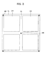
- a mark for coordinate measurement is arranged on a part corresponding to a so called scribe line, that is, a chip periphery region (a margin region when detaching a chip on a wafer by dicing).
- FIG. 3 is an example of a layout of arranging the marks for coordinate measurement on the scribe line. Coordinate measurement marks MK are arranged on the scribe line SL for sectionalizing the chip region.
- the method of the U.S. Patent No. 6040095 stands on an assumption that beam marks and an actual device pattern in a membrane displace by the same distortion function, so that disposition of the latter can be corrected based on measurement data of the former.
- this assumption is physically not self-evident, moreover, it became clear that it stood only approximately in our actual measurement.
- An object of the present invention is to provide a method of generating mask distortion data capable of improving accuracy of measuring distortion, an exposure method for more accurately correcting mask distortion for exposure by using the same, and a method of producing a semiconductor device using the same.
- a method of generating mask distortion data of a first thin film of a production mask formed with first positional accuracy measurement marks and having at least one first thin film formed with a transmittance portion and a blocking portion of a charged particle beam of a predetermined pattern comprising steps of obtaining a positional accuracy measurement mask by forming second positional accuracy measurement marks at substantially same positions as those of the first positional accuracy measurement marks on mask blanks having at least one second thin film, and forming third positional accuracy measurement marks on the second thin film; measuring positions of the second positional accuracy measurement marks and the third positional accuracy measurement marks of the positional accuracy measurement mask; calculating a correlation function between positions of the second positional accuracy measurement marks and the third positional accuracy measurement marks of the positional accuracy measurement mask; measuring positions of the first positional accuracy measurement marks of the production mask; and generating mask distortion data on the first thin film of the production mask from positions of the first positional accuracy measurement marks of the production mask by using the correlation function.
- the generation method of mask distortion data of the present invention as above is a method of generating mask distortion data of a first thin film of a production mask formed with first positional accuracy measurement marks and having at least one first thin film formed with a transmittance portion and a blocking portion of a charged particle beam of a predetermined pattern.
- a positional accuracy measurement mask is obtained by forming second positional accuracy measurement marks at substantially same positions as those of the first positional accuracy measurement marks on mask blanks having at least one second thin film, and forming third positional accuracy measurement marks on the second thin film.
- positions of the second positional accuracy measurement marks and the third positional accuracy measurement marks of the positional accuracy measurement mask are measured, and a correlation function between positions of the second positional accuracy measurement marks and the third positional accuracy measurement marks of the positional accuracy measurement masks is calculated.
- mask distortion data on the first thin film of the production mask is generated from positions of the first positional accuracy measurement marks of the production mask by using the correlation function.
- an exposure method for exposing a pattern by using a production mask formed with first positional accuracy measurement marks and having at least one first thin film formed with a transmittance portion and a blocking portion of a charged particle beam of the predetermined pattern comprising steps of obtaining a positional accuracy measurement mask by forming second positional accuracy measurement marks at substantially same positions as those of the first positional accuracy measurement marks on mask blanks having at least one second thin film, and forming third positional accuracy measurement marks on the second thin film; measuring positions of the second positional accuracy measurement marks and the third positional accuracy measurement marks of the positional accuracy measurement mask; calculating a correlation function between positions of the second positional accuracy measurement marks and the third positional accuracy measurement marks of the positional accuracy measurement mask; measuring positions of the first positional accuracy measurement marks of the production mask; generating mask distortion data on the first thin film of the production mask from positions of the first positional accuracy measurement marks of the production mask by using the correlation function; and exposing the pattern by using the production mask while correcting mask
- mask distortion data is generated by the above generation method of mask distortion data of the present invention, then, a pattern is exposed by using the production mask while correcting mask distortion on the first thin film based on the mask distortion data.
- a method of producing a semiconductor device including a step of exposing a pattern on a wafer to be exposed by using a production mask formed with first positional accuracy measurement marks and having at least one first thin film formed with a transmittance portion and a blocking portion of a charged particle beam of the predetermined pattern, comprising steps of obtaining a positional accuracy measurement mask by forming second positional accuracy measurement marks at substantially same positions as those of the first positional accuracy measurement marks on mask blanks having at least one second thin film, and forming third positional accuracy measurement marks on the second thin film; measuring positions of the second positional accuracy measurement marks and the third positional accuracy measurement marks of the positional accuracy measurement mask; calculating a correlation function between positions of the second positional accuracy measurement marks and the third positional accuracy measurement marks of the positional accuracy measurement mask; measuring positions of the first positional accuracy measurement marks of the production mask; generating mask distortion data on the first thin film of the production mask from positions of the first positional accuracy measurement marks of the production mask by using the correlation function; and exposing the pattern
- the production method of a semiconductor device of the present invention as above includes, after generating mask distortion data by the generation method of mask distortion data of the present invention as above, a step of exposing a pattern on a wafer to be exposed by using the production mask while correcting mask distortion on the first thin film based on the mask distortion data.
- the present embodiment relates to a method of generating distortion data of a mask, such as a PEL mask, for exposing by using a low energy electron beam proximity projection lithography (LEEPL) transfer apparatus, which is a method of generating mask distortion data according to a pattern formed on a first thin film of a production mask formed with first positional accuracy measurement marks and having at least one layer of first thin film formed with a transmittance portion and blocking portion of a charged particle beam of a predetermined pattern.
- LEEPL low energy electron beam proximity projection lithography
- the present embodiment relates to a method of exposing a pattern by correcting distortion based on the mask distortion data by using the above mask.
- FIG. 4 is a flowchart of a generation method of mask distortion data according to the present embodiment and an exposure method using the same.
- a positional accuracy measurement mask is formed by mask blanks having at least one layer of second thin film.
- the configuration of the positional accuracy measurement mask is the same as that of the production mask.
- the first thin film and the second thin film have the same layer configuration, and the positional accuracy measurement mask is formed with second positional accuracy measurement marks at substantially the same positions as those of the first positional accuracy measurement marks, and the second thin film is not formed with a pattern but third positional accuracy measurement marks.
- a second step ST12 positions of the second positional accuracy measurement marks and the third positional accuracy measurement marks of the positional accuracy measurement mask are measured by a coordinate measurement device, such as an LMS IPRO.
- a coordinate measurement device such as an LMS IPRO.
- IP data of the second positional accuracy measurement marks is obtained.
- IP data of the third positional accuracy measurement marks is obtained.
- a correlation function between the IP data of the second positional accuracy measurement marks and the IP data of the third positional accuracy measurement marks is calculated.
- the first step ST11 to the fifth step ST15 can be replaced by a finite element simulation modeling the mask.
- a production mask is formed by a mask blanks having at least one layer of a first thin film.
- the production mask is formed with first positional accuracy measurement marks as explained above, and a transmittance portion and blocking portion of a charged particle beam of a predetermined pattern are formed on the first thin film.
- a seventh step ST17 in the same way as in the second step ST12, positions of the first positional accuracy measurement marks of the production mask are measured by a coordinate measurement device, such as an LMS IPRO.
- a coordinate measurement device such as an LMS IPRO.
- IP data of the first positional accuracy measurement marks is obtained.
- a ninth step ST19 by using the correlation function between the IP data of the second positional accuracy measurement marks and the IP data of the third positional accuracy measurement marks obtained in the fifth step ST15, mask distortion data of the first thin film of the production mask is generated from the IP data of the first positional accuracy measurement marks obtained in the seventh step ST17.
- a condition of an exposure apparatus such as an EB deflection condition when exposing a pattern by using the production mask, is corrected based on the mask distortion data of the first thin film of the obtained production mask.
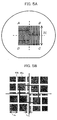
- FIG. 5A is a plan view of an appearance of the above production mask.
- the production mask has a square mask region having sides of 2L.
- the mask region is divided to four squares A to D respectively having sides of L, and each of them becomes one complementary mask.
- FIG. 5B is an enlarged view of a center portion of the mask region of FIG. 5A.
- a recessed portion 10a to be a small sectionalized membrane region having sides of L 10a is divided by a lattice shaped beam 10b having a width of L 10b .
- a pattern formed respectively on the small sectionalized membrane regions is omitted.
- a side L 10a of the recessed portion 10a is 1050 ⁇ m
- the width L 10b of the beam is 200 ⁇ m
- a side 2L of the overall mask region is 40 mm.
- FIG. 6 is a schematic sectional view of the above production mask.
- a buried oxide film (BOX) 11 as an interlayer having an etching stopper function and a first silicon thin film (SOI: silicon on insulator) 12 to be a membrane are formed on a silicon substrate 10.
- a part of the silicon substrate 10 corresponding to the membrane is etched from the back surface to be formed with recessed portion 10a sectionalized to be a lattice shape to configure the lattice shaped beam 10b.
- the SOI layer 12 on the region of the recessed portions 10a sectionalized by the lattice shaped beam 10b is formed through holes P along a mask pattern.
- first positional accuracy measurement marks MK1 are formed on the SOI layer 10.
- FIG. 7 is a plan view of a layout of positional accuracy measurement marks of the above production mask.
- the first positional accuracy measurement marks MK1 are formed on a region for forming the lattice shaped beam 10b for sectionalizing the recessed portions 10a to be small sectionalized membrane regions.
- the first positional accuracy measurement marks MK1 may be formed on the SOI layer 12 positioned above the beam 10b as shown in FIG. 6 or on the surface of the beam 10b on the opposite surface from the surface to be formed the SOI layer 12 as far as they are on the lattice shaped beam 10b formation region. It can be selected, for example, in accordance with the posture at the time of measuring positions of the first positional accuracy measurement marks MK1.
- the positional accuracy measurement mask has the same configuration as that of the above production mask, but is different in the point that third positional accuracy measurement marks MK3 are formed instead of through holes along the mask pattern on the SOI layer on the recessed portion 10a.
- the positional accuracy measurement mask will be explained with reference to FIG. 6 and FIG. 7.
- a BOX layer 11 and a second thin film (SOI) 12' are stacked on a silicon substrate 10, a part of the silicon substrate corresponding to a membrane is etched from the back surface to form recessed portions 10a sectionalized to be a lattice shape, so a lattice shaped beam 10b is configured.
- second positional accuracy measurement marks MK2 are formed on the formation region of the lattice shaped beam 10b in the same way as in the first positional accuracy measurement marks MK1.
- the SOI layer 12' on the region of the recessed portions 10a sectionalized by the lattice shaped beam 10b is formed third positional accuracy measurement marks MK3. Detailed illustration is omitted in FIG. 7.
- first positional accuracy measurement marks MK1 and the second positional accuracy measurement marks MK2 for example, twenty marks are formed on the formation region of the beam 10b around the region divided as one recessed portion. In this way, much larger number of marks can be arranged than the number of marks in the related art shown in FIG. 3, so that distortion of a higher order can be measured by this and terms of a higher order other than linear components can be corrected.
- the third positional accuracy measurement marks MK3 for example, 3 ⁇ 3 number of square marks by 6 ⁇ m by 6 ⁇ m are arranged at pitches of 500 ⁇ m in each recessed portion 10a sectionalized to be a lattice shape.
- the production mask and the positional accuracy measurement mask can be formed in the same way.
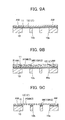
- an SOI wafer formed by stacking a buried oxide film (BOX layer) 11 as an interlayer having an etching stopper function and a silicon layer (SOI layer) 12 to be a membrane on a silicon substrate 10 is prepared.
- the whole surface of the SOI wafer is covered with a natural oxide film 13.
- the SOI layer 12 is removed until reaching to the BOX layer 11 to be a predetermined pattern on the periphery portion of the SOI wafer so as to form alignment marks AM.
- a resist film (not shown) is formed on the back surface of the silicon substrate, openings of a pattern of a lattice shape is formed by exposure and development, etching processing, such as RIE (reactive ion etching), is performed to form a recessed portion 10a reaching to the BOX layer 11 from the back surface of the silicon substrate 10, for example, of a pattern sectionalized to be a lattice shape.
- etching processing such as RIE (reactive ion etching)
- RIE reactive ion etching
- a resist film (not shown) is removed by ashing processing, etc. and oxide silicon on a portion exposed on the surface is removed by wet etching by an HF solution. Namely, the natural oxide film 13 and the BOX film 11 exposed on the bottom portion of the recessed portion 10a are removed.
- mask blanks configured by stacking the BOX layer 11 and the SOI layer 12 on the silicon substrate 10 wherein a recessed portion sectionalized to be a lattice shape is formed to an extent the SOI layer exposes from the back side of the silicon substrate 10.
- a resist film R is formed on the SOI layer 12, and a pattern P is formed by exposing, for example, by an electron beam and developing along mask data of a mask to be formed in the method of producing the production mask.
- a pattern for the first positional accuracy measurement marks MK1 are also formed on the resist film R.
- dry etching such as RIE
- RIE reactive ion etching
- the resist film R is removed by ashing processing, so that a mask having the configuration shown in FIG. 9C can be produced.
- mask blanks are formed by stacking the BOX layer 11 and the SOI layer 12' on the silicon substrate 10 as shown in FIG. 9A, and a pattern of the second positional accuracy measurement marks MK2 and the third positional accuracy measurement marks MK3 is obtained by exposing and developing along the pattern of the second positional accuracy measurement marks MK2 and the third positional accuracy measurement marks MK3 as shown in FIG. 9B.
- distortion data of a production mask can be generated by a procedure shown in the flowchart in FIG. 4 by using the production mask and the positional accuracy measurement mask formed as above.
- Mask distortion data generated as such can improve accuracy of measuring distortion due to the reasons explained later on.
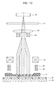
- FIG. 10 is a schematic view of an exposure system used in the LEEPL.
- the exposure system comprises an electron gun 30, an aperture 31, a condenser lens 32, a pair of main deflection lenses (33, 34) and a pair of sub deflection lenses (35, 36).
- An electron beam EB having a current value of 5.5 ⁇ A and a beam diameter of 300 ⁇ m accelerated at an EB acceleration voltage of 2keV emitted from the electron gun 30 is limited by the aperture 31 and made to be a parallel beam by the condenser lens 32.
- the main deflection lenses (33, 34) deflect the electron beam, so that the electron beam EB perpendicularly irradiates the stencil mask 37 while being in parallel.
- the electron beam EB is incident on the stencil mask 37 in a raster or vector scanning mode, and the main deflection lenses (33, 34) are used for deflecting the electron beam EB in both cases.
- the sub deflection lenses (35, 36) further precisely adjust the electron beam EB deflected by the main deflection lenses (33, 34).
- the electron beam EB transmitted through the stencil mask 37 is incident on the resist film 39 provided, for example, on a silicon wafer 38 and pattern exposure is performed thereon.
- the present embodiment based on the obtained distortion data of the production mask, it is possible to perform pattern exposure while more precisely correcting mask distortion by using the production mask, for example, correcting the condition of the sub deflection lenses (35, 36), and exposing under the corrected condition.
- a generation method of mask distortion data of the present embodiment was applied to a PEL mask for generating mask distortion data.
- a thickness of the wafer substrate was 381 ⁇ m (polished on both surfaces to improve flatness of the mask), a thickness of the BOX layer was 400 nm, a thickness of the SOI layer was 600 nm, and internal stress of the membrane layer was adjusted to 10 MPa by injecting boron (B) atoms of 10 19 /cm 3 .
- the production mask and the positional accuracy measurement mask having the configurations shown in FIG. 5 and FIG. 6 were formed by steps shown in FIG. 8A to FIG. 8C and FIG. 9A to FIG. 9C.
- first positional accuracy measurement marks MK1 on the production mask and second positional accuracy measurement marks MK2 on the positional accuracy measurement mask were configured the same and formed on a formation region of the beam 10b.
- a pattern P of a mask to be formed was transferred on the SOI layer on the region of the recessed portions sectionalized to be a lattice shape on the production mask, and a pattern of third positional accuracy measurement marks were transferred on the positional accuracy measurement mask.
- FIG. 11A is a plan view of the above frame, and FIG. 11B is a sectional view thereof.
- a frame 20 has a ring shape having an outer diameter of 20a and an inner diameter of 20b, and a step 20c is formed at a position of a predetermined diameter.
- the inner diameter is designed to be wider than the whole mask region having sides of 2L.
- the production mask and the positional accuracy measurement mask were respectively adhered to the above frame with an epoxy resin.
- positions of the second positional accuracy measurement marks formed on a formation region of a lattice shaped beam and the three positional accuracy measurement marks formed on the SOI layer on the recessed portion formation region sectionalized by the lattice shaped beam were respectively measured by a coordinate measurement device (LMS IPRO), and IP data of the second positional accuracy measurement marks and IP data of the third positional accuracy measurement marks were obtained.
- LMS IPRO coordinate measurement device
- a mask holding cassette was newly produced to measure positional accuracy of the positional accuracy measurement mask and the production mask when measuring positions by the coordinate measurement device.
- FIG. 12A is a plan view of the mask holding cassette
- FIG. 12B is a schematic sectional view when holding a mask by the mask holding cassette.
- the mask holding cassette 21 is provided with an electrostatic chuck 21a and thereby an outer circumference portion other than the mask region 21b (40 mm square at the center in this case) is electrostatically chucked. And measurement is made in a state that the SOI layer (second thin film) 12' faces upward and the mask is held from the opposite side of the SOI layer (second thin film) 12'. Note that in FIG. 12B, illustration of the second positional accuracy measurement marks is omitted.
- it may be configured to be provided with a suction chuck instead of the electrostatic chuck.
- IP accuracy of marks can be measured in a state that the stencil mask is made to be flat.
- FIG. 13A is a graph of the measurement result of the second positional accuracy measurement marks MK2 formed on the beam formation region, wherein solid lines are made by connecting actually measured values and broken lines indicate positions of an ideal lattice.
- FIG. 13B is a graph of measurement results of the third positional accuracy measurement marks MK3 formed on the SOI layer on the region of the recessed portions sectionalized to be a lattice shape, wherein solid lines are made by connecting actually measured values and broken lines indicate positions of an ideal lattice.
- IP measurement results of the second positional accuracy measurement marks MK2 formed on the beam formation region and the third positional accuracy measurement marks MK3 formed on the SOI layer on the region of the recessed portions sectionalized to be a lattice shape are similar and seem to qualitatively support an idea of the related art (the U.S. Patent No. 6040095), however, when closely analyzing the data, a difference of about 20 nm at maximum was found between them.
- the error is 5 nm in the 1/4 reduction projection method, such as the EPL, and 20 nm in the PEL on the wafer. Since an error being unacceptable even in the 1/4 reduction production method is generated in the related art, it cannot be used in the PEL as an unmagnification method used in the present embodiment.
- the fixing methods are not completely the same on the two stages, so that a shape of the mask (projections and recesses) of the mask differs in accordance with difference of degrees to straighten warps of the mask.
- the second positional accuracy measurement marks MK2 formed on the beam formation region basically indicate displacement within the plane of (tilting angle of mask substrate) x (half of substrate thickness) as described in articles of mechanics of materials (for example, refer to "Theory of Plates and Shells" by S. P. Timoshenko and S. Woinowsky-Krieger).
- a correlation function between the IP data of the second positional accuracy measurement marks and the IP data of the third positional accuracy measurement marks was calculated from the two data shown in FIG. 13A and FIG. 13B.
- the correlation function was calculated on an experimental basis, but the process can be substituted by highly accurate finite element simulation.
- the first positional accuracy measurement marks formed on the formation region of the lattice shaped beam were measured by the coordinate measurement device (LMS IPRO) and IP data thereof was obtained on the production mask. Note that illustration of the first positional accuracy measurement marks are omitted in FIG. 12B.
- the production mask was held by using the same cassette used in measuring the positional accuracy measurement mask.
- FIG. 14 is a graph of measurement results of the first positional accuracy measurement marks MK1 formed on the beam formation region, wherein solid lines are made by connecting actually measured values, broken lines indicate positions of an ideal lattice, and errors are enlarged in the same way as the above so that deviation from the ideal lattice is easily seen.
- a correlation function of a distortion function obtained form the second positional accuracy measurement marks MK2 formed on the beam formation region on the positional accuracy measurement mask and the third positional accuracy measurement marks MK3 formed on the SOI layer on the region of the recessed portions sectionalized to be a lattice shape is examined in advance, and an IP error of the first positional accuracy measurement marks MK1 formed on the beam formation region are converted to an IP error of a pattern on the SOI layer of the production mask, and used.
- the mask distortion data after generating mask distortion data on the SOI layer (first thin film) of the production mask, it is preferable to correct the mask distortion data by using a function indicating distortion generated on the positional accuracy measurement mask and production mask at the time the second thin film and the first thin film facing upward were made to face downward in both of the positional accuracy measurement mask and the production mask.
- the distortion data of the production mask obtained in the first embodiment is data in a state that the SOI layer faces upward. But the SOI layer faces downward in an actual exposure step, so the accuracy is furthermore improved when creating the sub deflection correction data after converting to data in the downward state by the ITF.
- the inversion of the mask posture between the time of IP measurement and the time of exposure of the mask is corrected by the ITF, but there is another method of dealing the mask posture in the IP measurement step same as that in exposure step.
- positions of the first to third positional accuracy measurement marks (MK1 to MK3) on the positional accuracy measurement mask and the production mask when being held in the cassette in a state that the first thin film or the second thin film faces downward, positions can be measured by the posture that the first thin film or the second thin film faces downward, which is the same as the posture in the exposure step. Therefore, when measuring positions in this state, more accurate measurement of the positions can be attained without using the ITF and a mask distortion function can be generated.
- a mask is loaded facing downward, but a face to be electrostatically chucked is different, so that it is preferable to use separately designed cassettes for measuring positions in the same state with the exposure posture as much as possible.
- FIG. 15 is a schematic sectional view when holding a PEL mask in a mask holding cassette for an EPL mask.
- the mask holding cassette 22 is provided with an electrostatic chuck 22a, wherein recessed portions 22b are formed on the mask region and an outer circumferential portion other than the recessed portion is electrostatically chucked.
- it may be configured to be provided with a suction chuck instead of the electrostatic chuck.
- FIG. 16 is a schematic sectional view when holding a PEL mask in a mask holding cassette for a PEL mask.
- the mask holding cassette is provided with an electrostatic chuck 23a, and an outer circumferential portion other than the mask region 23b is electrostatically chucked thereby. Measurement is made in a state that the SOI layer (12, 12') faces downward and is supported from the opposite side of the SOI layer (12, 12') and inserted in the case 24. Note that illustration of the first and second positional accuracy measurement marks are omitted in FIG. 16.
- it may be configured to be provided with a suction chuck instead of the electrostatic chuck.
- the above production method of a mask of the present embodiment can be applied to a production method of a semiconductor device.
- distortion data of the production mask is calculated by the generation method of mask distortion data according to the present embodiment.
- a correction condition of a sub deflection lens of an EB to correct the obtained distortion data is obtained, pattern exposure is performed by using the production mask, and a pattern formed on the mask is transferred on a photosensitive face.
- a semiconductor device can be produced by applying the production method of a mask of the present embodiment.
- the present invention is not limited to the above embodiment.
- a stencil mask (PEL mask) was explained, but by applying a well known mask production process disclosed in various papers and patents, it can be made to be a mask for NGL.
- the present invention can be applied not only to the PEL mask, but also to an EPL mask.
- the generation method of mask distortion data and the exposure method of the present invention can be applied as a generation method of mask distortion data and an exposure method using the same for performing pattern exposure in a production method of a semiconductor device having a step of performing pattern exposure on a wafer to be exposed.
- the method of generating mask distortion data of the present invention is capable of improving accuracy of measuring distortion.
- the exposure method of the present invention is capable of performing exposure by more accurately correcting mask distortion by using the generation method of mask distortion data of the present invention.
- the method of producing a semiconductor device of the present invention is capable of producing a semiconductor device by using the generation method of mask distortion data of the present invention and the exposure method using the same.
Landscapes
- Physics & Mathematics (AREA)
- General Physics & Mathematics (AREA)
- Chemical & Material Sciences (AREA)
- Analytical Chemistry (AREA)
- Electron Beam Exposure (AREA)
- Preparing Plates And Mask In Photomechanical Process (AREA)
- Exposure And Positioning Against Photoresist Photosensitive Materials (AREA)
- Length-Measuring Devices Using Wave Or Particle Radiation (AREA)
- Exposure Of Semiconductors, Excluding Electron Or Ion Beam Exposure (AREA)
Applications Claiming Priority (2)
| Application Number | Priority Date | Filing Date | Title |
|---|---|---|---|
| JP2003153251 | 2003-05-29 | ||
| JP2003153251A JP4046012B2 (ja) | 2003-05-29 | 2003-05-29 | マスク歪データの生成方法、露光方法および半導体装置の製造方法 |
Publications (2)
| Publication Number | Publication Date |
|---|---|
| EP1482374A2 true EP1482374A2 (fr) | 2004-12-01 |
| EP1482374A3 EP1482374A3 (fr) | 2007-05-30 |
Family
ID=33128288
Family Applications (1)
| Application Number | Title | Priority Date | Filing Date |
|---|---|---|---|
| EP04012335A Withdrawn EP1482374A3 (fr) | 2003-05-29 | 2004-05-25 | Méthode de génération de données de distorsion d'un masque, méthode d'exposition et méthode de fabrication d'un dispositif semiconducteur |
Country Status (5)
| Country | Link |
|---|---|
| US (1) | US7175952B2 (fr) |
| EP (1) | EP1482374A3 (fr) |
| JP (1) | JP4046012B2 (fr) |
| KR (1) | KR20040103411A (fr) |
| TW (1) | TWI249775B (fr) |
Cited By (1)
| Publication number | Priority date | Publication date | Assignee | Title |
|---|---|---|---|---|
| EP1564793A1 (fr) * | 2002-11-14 | 2005-08-17 | Sony Corporation | Dispositif d'exposition, procede d'exposition et procede de fabrication de dispositifs a semi-conducteur |
Families Citing this family (24)
| Publication number | Priority date | Publication date | Assignee | Title |
|---|---|---|---|---|
| JP3675421B2 (ja) * | 2002-03-28 | 2005-07-27 | ソニー株式会社 | マスクパターン補正方法、マスク製造方法、マスクおよび半導体装置の製造方法 |
| JP4401691B2 (ja) * | 2003-06-13 | 2010-01-20 | 株式会社オクテック | 電子ビーム照射管の電子ビーム透過窓の製造方法 |
| KR101100003B1 (ko) * | 2004-03-09 | 2011-12-28 | 호야 가부시키가이샤 | 마스크 블랭크 생산 시스템 |
| JP2006235327A (ja) * | 2005-02-25 | 2006-09-07 | Toshiba Corp | マスクパターンデータ・マスク検査データ作成方法、及びフォトマスクの製造・検査方法 |
| DE102007042272B4 (de) * | 2007-09-06 | 2009-09-24 | Vistec Semiconductor Systems Gmbh | Verfahren zur Korrektur der durch die Verzeichnung eines Objektivs verursachten Messfehler |
| US20120219886A1 (en) | 2011-02-28 | 2012-08-30 | D2S, Inc. | Method and system for forming patterns using charged particle beam lithography with variable pattern dosage |
| US8057970B2 (en) | 2008-09-01 | 2011-11-15 | D2S, Inc. | Method and system for forming circular patterns on a surface |
| US8473875B2 (en) | 2010-10-13 | 2013-06-25 | D2S, Inc. | Method and system for forming high accuracy patterns using charged particle beam lithography |
| US8039176B2 (en) | 2009-08-26 | 2011-10-18 | D2S, Inc. | Method for fracturing and forming a pattern using curvilinear characters with charged particle beam lithography |
| US7901850B2 (en) | 2008-09-01 | 2011-03-08 | D2S, Inc. | Method and system for design of a reticle to be manufactured using variable shaped beam lithography |
| US9341936B2 (en) | 2008-09-01 | 2016-05-17 | D2S, Inc. | Method and system for forming a pattern on a reticle using charged particle beam lithography |
| US9323140B2 (en) | 2008-09-01 | 2016-04-26 | D2S, Inc. | Method and system for forming a pattern on a reticle using charged particle beam lithography |
| JP5429864B2 (ja) * | 2009-07-24 | 2014-02-26 | 独立行政法人物質・材料研究機構 | 歪み計測用パターン |
| US8404404B2 (en) * | 2009-08-21 | 2013-03-26 | D2S, Inc. | Method and system for manufacturing a surface using character projection lithography with variable magnification |
| US9164372B2 (en) | 2009-08-26 | 2015-10-20 | D2S, Inc. | Method and system for forming non-manhattan patterns using variable shaped beam lithography |
| US9448473B2 (en) | 2009-08-26 | 2016-09-20 | D2S, Inc. | Method for fracturing and forming a pattern using shaped beam charged particle beam lithography |
| US9612530B2 (en) | 2011-02-28 | 2017-04-04 | D2S, Inc. | Method and system for design of enhanced edge slope patterns for charged particle beam lithography |
| US9057956B2 (en) | 2011-02-28 | 2015-06-16 | D2S, Inc. | Method and system for design of enhanced edge slope patterns for charged particle beam lithography |
| WO2012148606A2 (fr) | 2011-04-26 | 2012-11-01 | D2S, Inc. | Procédé et système de formation de motifs de type non manhattan par lithographie à faisceau formé variable |
| US9034542B2 (en) | 2011-06-25 | 2015-05-19 | D2S, Inc. | Method and system for forming patterns with charged particle beam lithography |
| WO2013158574A1 (fr) | 2012-04-18 | 2013-10-24 | D2S, Inc. | Procédé et système pour uniformité de dimension critique utilisant la lithographie par faisceaux de particules chargées |
| WO2013158573A1 (fr) | 2012-04-18 | 2013-10-24 | D2S, Inc. | Procédé et système de formation de motifs par utilisation de lithographie par faisceau de particules chargées |
| US9343267B2 (en) | 2012-04-18 | 2016-05-17 | D2S, Inc. | Method and system for dimensional uniformity using charged particle beam lithography |
| JP5983218B2 (ja) * | 2012-09-11 | 2016-08-31 | 大日本印刷株式会社 | ナノインプリントリソグラフィ用テンプレートの製造方法 |
Citations (3)
| Publication number | Priority date | Publication date | Assignee | Title |
|---|---|---|---|---|
| US6040095A (en) * | 1998-09-30 | 2000-03-21 | Nikon Corporation | Measurement marks for e-beam projection mask and method of using |
| EP1083462A1 (fr) * | 1998-03-26 | 2001-03-14 | Nikon Corporation | Procede et systeme d'exposition, photomasque et son procede de fabrication, micro-composant et son procede de fabrication |
| US6277532B1 (en) * | 1998-10-14 | 2001-08-21 | Nikon Corporation | Charged-particle-beam microlithographic methods for correction of reticle distortions |
Family Cites Families (2)
| Publication number | Priority date | Publication date | Assignee | Title |
|---|---|---|---|---|
| US6180289B1 (en) * | 1997-07-23 | 2001-01-30 | Nikon Corporation | Projection-microlithography mask with separate mask substrates |
| JP2002222750A (ja) * | 2001-01-24 | 2002-08-09 | Nec Corp | 電子ビーム転写用マスク |
-
2003
- 2003-05-29 JP JP2003153251A patent/JP4046012B2/ja not_active Expired - Fee Related
-
2004
- 2004-05-19 US US10/848,918 patent/US7175952B2/en not_active Expired - Fee Related
- 2004-05-25 EP EP04012335A patent/EP1482374A3/fr not_active Withdrawn
- 2004-05-28 KR KR1020040038156A patent/KR20040103411A/ko not_active Application Discontinuation
- 2004-05-28 TW TW093115198A patent/TWI249775B/zh not_active IP Right Cessation
Patent Citations (3)
| Publication number | Priority date | Publication date | Assignee | Title |
|---|---|---|---|---|
| EP1083462A1 (fr) * | 1998-03-26 | 2001-03-14 | Nikon Corporation | Procede et systeme d'exposition, photomasque et son procede de fabrication, micro-composant et son procede de fabrication |
| US6040095A (en) * | 1998-09-30 | 2000-03-21 | Nikon Corporation | Measurement marks for e-beam projection mask and method of using |
| US6277532B1 (en) * | 1998-10-14 | 2001-08-21 | Nikon Corporation | Charged-particle-beam microlithographic methods for correction of reticle distortions |
Cited By (2)
| Publication number | Priority date | Publication date | Assignee | Title |
|---|---|---|---|---|
| EP1564793A1 (fr) * | 2002-11-14 | 2005-08-17 | Sony Corporation | Dispositif d'exposition, procede d'exposition et procede de fabrication de dispositifs a semi-conducteur |
| EP1564793A4 (fr) * | 2002-11-14 | 2010-01-13 | Sony Corp | Dispositif d'exposition, procede d'exposition et procede de fabrication de dispositifs a semi-conducteur |
Also Published As
| Publication number | Publication date |
|---|---|
| US20050014076A1 (en) | 2005-01-20 |
| JP4046012B2 (ja) | 2008-02-13 |
| US7175952B2 (en) | 2007-02-13 |
| KR20040103411A (ko) | 2004-12-08 |
| EP1482374A3 (fr) | 2007-05-30 |
| TW200509206A (en) | 2005-03-01 |
| JP2004356440A (ja) | 2004-12-16 |
| TWI249775B (en) | 2006-02-21 |
Similar Documents
| Publication | Publication Date | Title |
|---|---|---|
| US7175952B2 (en) | Method of generating mask distortion data, exposure method and method of producing semiconductor device | |
| US7126231B2 (en) | Mask-making member and its production method, mask and its making method, exposure process, and fabrication method of semiconductor device | |
| US7202488B2 (en) | Correction system, method of correcting deflection distortion, program and method for manufacturing a semiconductor device | |
| JP3791484B2 (ja) | 露光方法および半導体装置の製造方法 | |
| US6583430B1 (en) | Electron beam exposure method and apparatus | |
| JP3675421B2 (ja) | マスクパターン補正方法、マスク製造方法、マスクおよび半導体装置の製造方法 | |
| US5800949A (en) | Mask, method of producing a device using the mask and aligner with the mask | |
| US6741732B2 (en) | Exposure method and device manufacturing method using this exposure method | |
| JP2002305138A (ja) | 露光装置および露光方法 | |
| JP3445102B2 (ja) | 露光装置およびデバイス製造方法 | |
| US6381005B1 (en) | Mask holding device, exposure apparatus and device manufacturing method | |
| US20060108541A1 (en) | Alignment method, alignment substrate, production method for alignment substrate, exposure method, exposure system and mask producing method | |
| JP2004235221A (ja) | マスクの製造方法、パターンの形成方法、歪計測用フォトマスクおよび半導体装置の製造方法 | |
| US20020127865A1 (en) | Lithography method for forming semiconductor devices with sub-micron structures on a wafer and apparatus | |
| JPH10289870A (ja) | 半導体露光装置およびデバイス製造方法 | |
| JP2005175167A (ja) | 露光装置および露光方法、並びにプログラムおよびマスク精度保証方法 | |
| JP2005181044A (ja) | 座標測定精度較正方法、座標測定精度評価方法、プログラムおよびマスク | |
| JP3633554B2 (ja) | マスクおよびその製造方法と半導体装置の製造方法 | |
| JP2004158681A (ja) | マスク、露光装置および露光方法 | |
| JP2003142439A (ja) | ウェハの研磨方法及びマスク | |
| JP2000260690A (ja) | X線露光装置 | |
| JP2006147871A (ja) | 重ね合わせ露光方法 | |
| US20030085363A1 (en) | Methods for detecting incidence orthogonality of a patterned beam in charged-particle-beam (CPB) microlithography, and CPB microlithography systems that perform same | |
| Reu | Comparative analysis of next generation lithography masks: PREVAIL and SCALPEL technologies | |
| JP2002367887A (ja) | パターン転写用マスク、パターン転写方法、露光方法、半導体装置の製造方法及び半導体装置 |
Legal Events
| Date | Code | Title | Description |
|---|---|---|---|
| PUAI | Public reference made under article 153(3) epc to a published international application that has entered the european phase |
Free format text: ORIGINAL CODE: 0009012 |
|
| AK | Designated contracting states |
Kind code of ref document: A2 Designated state(s): AT BE BG CH CY CZ DE DK EE ES FI FR GB GR HU IE IT LI LU MC NL PL PT RO SE SI SK TR |
|
| AX | Request for extension of the european patent |
Extension state: AL HR LT LV MK |
|
| PUAL | Search report despatched |
Free format text: ORIGINAL CODE: 0009013 |
|
| AK | Designated contracting states |
Kind code of ref document: A3 Designated state(s): AT BE BG CH CY CZ DE DK EE ES FI FR GB GR HU IE IT LI LU MC NL PL PT RO SE SI SK TR |
|
| AX | Request for extension of the european patent |
Extension state: AL HR LT LV MK |
|
| AKX | Designation fees paid | ||
| STAA | Information on the status of an ep patent application or granted ep patent |
Free format text: STATUS: THE APPLICATION IS DEEMED TO BE WITHDRAWN |
|
| 18D | Application deemed to be withdrawn |
Effective date: 20071201 |
|
| REG | Reference to a national code |
Ref country code: DE Ref legal event code: 8566 |