EP1480239A2 - Verfahren und Schaltungsanordnung zur Funktionsüberwachung eines elektronisch-mechanischen Positionsschalters - Google Patents
Verfahren und Schaltungsanordnung zur Funktionsüberwachung eines elektronisch-mechanischen Positionsschalters Download PDFInfo
- Publication number
- EP1480239A2 EP1480239A2 EP04010136A EP04010136A EP1480239A2 EP 1480239 A2 EP1480239 A2 EP 1480239A2 EP 04010136 A EP04010136 A EP 04010136A EP 04010136 A EP04010136 A EP 04010136A EP 1480239 A2 EP1480239 A2 EP 1480239A2
- Authority
- EP
- European Patent Office
- Prior art keywords
- output
- microcontroller
- switching contact
- state
- watchdog
- Prior art date
- Legal status (The legal status is an assumption and is not a legal conclusion. Google has not performed a legal analysis and makes no representation as to the accuracy of the status listed.)
- Granted
Links
- 238000012544 monitoring process Methods 0.000 title claims abstract description 30
- 238000000034 method Methods 0.000 title claims description 29
- 238000012360 testing method Methods 0.000 claims abstract description 61
- 230000007704 transition Effects 0.000 claims abstract description 33
- 101001135344 Homo sapiens Polypyrimidine tract-binding protein 1 Proteins 0.000 claims description 17
- 102100033073 Polypyrimidine tract-binding protein 1 Human genes 0.000 claims description 17
- 230000003287 optical effect Effects 0.000 claims description 2
- 230000000737 periodic effect Effects 0.000 claims description 2
- 230000003213 activating effect Effects 0.000 abstract 1
- 230000008859 change Effects 0.000 description 8
- 230000007547 defect Effects 0.000 description 8
- 239000003990 capacitor Substances 0.000 description 7
- 108010076504 Protein Sorting Signals Proteins 0.000 description 4
- 230000007257 malfunction Effects 0.000 description 4
- 238000011161 development Methods 0.000 description 3
- 230000018109 developmental process Effects 0.000 description 3
- 238000010586 diagram Methods 0.000 description 3
- 230000002093 peripheral effect Effects 0.000 description 3
- 230000009885 systemic effect Effects 0.000 description 3
- 238000011144 upstream manufacturing Methods 0.000 description 3
- 230000005540 biological transmission Effects 0.000 description 2
- 230000006835 compression Effects 0.000 description 2
- 238000007906 compression Methods 0.000 description 2
- 230000001419 dependent effect Effects 0.000 description 2
- 230000004044 response Effects 0.000 description 2
- 101100243745 Schizosaccharomyces pombe (strain 972 / ATCC 24843) ptb1 gene Proteins 0.000 description 1
- 230000033228 biological regulation Effects 0.000 description 1
- 238000012790 confirmation Methods 0.000 description 1
- 230000001934 delay Effects 0.000 description 1
- 230000003111 delayed effect Effects 0.000 description 1
- 238000001514 detection method Methods 0.000 description 1
- 238000005516 engineering process Methods 0.000 description 1
- 230000003628 erosive effect Effects 0.000 description 1
- 238000011156 evaluation Methods 0.000 description 1
- 230000036039 immunity Effects 0.000 description 1
- 230000006872 improvement Effects 0.000 description 1
- 230000001788 irregular Effects 0.000 description 1
- 230000000873 masking effect Effects 0.000 description 1
- 239000000463 material Substances 0.000 description 1
- 150000003071 polychlorinated biphenyls Chemical class 0.000 description 1
- 230000008569 process Effects 0.000 description 1
- 239000000047 product Substances 0.000 description 1
- 238000012552 review Methods 0.000 description 1
- 238000000926 separation method Methods 0.000 description 1
- 230000011664 signaling Effects 0.000 description 1
- 239000013589 supplement Substances 0.000 description 1
- 230000001629 suppression Effects 0.000 description 1
- 239000000725 suspension Substances 0.000 description 1
- 238000012546 transfer Methods 0.000 description 1
- 238000012795 verification Methods 0.000 description 1
Images



Classifications
-
- H—ELECTRICITY
- H01—ELECTRIC ELEMENTS
- H01H—ELECTRIC SWITCHES; RELAYS; SELECTORS; EMERGENCY PROTECTIVE DEVICES
- H01H9/00—Details of switching devices, not covered by groups H01H1/00 - H01H7/00
- H01H9/54—Circuit arrangements not adapted to a particular application of the switching device and for which no provision exists elsewhere
- H01H9/547—Combinations of mechanical switches and static switches, the latter being controlled by the former
-
- G—PHYSICS
- G01—MEASURING; TESTING
- G01D—MEASURING NOT SPECIALLY ADAPTED FOR A SPECIFIC VARIABLE; ARRANGEMENTS FOR MEASURING TWO OR MORE VARIABLES NOT COVERED IN A SINGLE OTHER SUBCLASS; TARIFF METERING APPARATUS; MEASURING OR TESTING NOT OTHERWISE PROVIDED FOR
- G01D5/00—Mechanical means for transferring the output of a sensing member; Means for converting the output of a sensing member to another variable where the form or nature of the sensing member does not constrain the means for converting; Transducers not specially adapted for a specific variable
- G01D5/12—Mechanical means for transferring the output of a sensing member; Means for converting the output of a sensing member to another variable where the form or nature of the sensing member does not constrain the means for converting; Transducers not specially adapted for a specific variable using electric or magnetic means
- G01D5/14—Mechanical means for transferring the output of a sensing member; Means for converting the output of a sensing member to another variable where the form or nature of the sensing member does not constrain the means for converting; Transducers not specially adapted for a specific variable using electric or magnetic means influencing the magnitude of a current or voltage
- G01D5/16—Mechanical means for transferring the output of a sensing member; Means for converting the output of a sensing member to another variable where the form or nature of the sensing member does not constrain the means for converting; Transducers not specially adapted for a specific variable using electric or magnetic means influencing the magnitude of a current or voltage by varying resistance
- G01D5/165—Mechanical means for transferring the output of a sensing member; Means for converting the output of a sensing member to another variable where the form or nature of the sensing member does not constrain the means for converting; Transducers not specially adapted for a specific variable using electric or magnetic means influencing the magnitude of a current or voltage by varying resistance by relative movement of a point of contact or actuation and a resistive track
Definitions
- the invention relates to a method and a circuit arrangement for monitoring function an electronic-mechanical position switch according to the generic terms the independent claims.
- position switch AT is an electromechanical Position switch described.
- mechanical switching contacts For example, couples or individual contacts of openers and / or closers arranged and a longitudinally displaceable butt tappet for immediate mechanical Operation of the switching contacts stored.
- head tappets replaceable drive heads purposed. So can on the housing of the position switch optionally a Drive head fixed with swivel lever, roller lever, adjusting roller lever or spring rod become.
- An electronic-mechanical position switch is from the utility model DE 202 03 214 U1 known.
- a housing In a housing are an actuating tappet, a potentiometer, a microcontroller and electronic switch contacts arranged.
- the actuating tappet is coupled to the wiper of the potentiometer.
- the microcontroller At ram actuation the microcontroller is supplied with a changing electrical signal, the when the programmed threshold exceeds or falls below a change of state causes the switching contacts.
- the switching contacts are output side connected to the terminals.
- To set the switching point proposed via a programming terminal or via selector switch To program a threshold value or from a number stored in the microcontroller selected thresholds. There are no details about it made as failures of the electronics can be detected to prevent erroneous output signals to faulty controls on the periphery of the position switch to lead.
- the invention is therefore the function monitoring of an electronic-mechanical Position switch based as task.
- the method according to the invention tests the watchdog monitoring on the one hand and the breaking capacity of the at least one electronic switching contact on the other hand.
- the watchdog monitoring is used to detect failures of the microcontroller and to safely transfer the switching contact to the open state to avoid faulty control at the periphery of the position switch.
- watchdog signals are generated in a known manner by the microcontroller, which can be concluded in the absence of a failure of the microcontroller.
- “AbschaltTAL” is meant that when the switching point is exceeded by the plunger in the corresponding direction of the hitherto closed switch contact actually opens.
- steps C and D When testing the breaking capacity, it is checked in steps C and D whether the switching contact which is in the closed state is capable of being opened.
- the closed state of the electronic switching contact is effected in the event of functionality by the closing signal level of the control signal. However, it may occur during the output of the closing control signal component failure on the way from the output of the microcontroller to the switching contact, as a result, the switching contact can no longer assume the open state, for example due to the fürlegierens the output electrodes of the electronic switching contact. Such failures must be detected early, since under certain circumstances, the actuating tappet does not go through the switching point for a long time.
- the first and the second test intervals occur in periodic Intervals, preferably after a time interval, 500 to 1200 program cycles of the microcontroller, which corresponds to a test period of 2 to 6 seconds.
- An advantageous development of the method according to the invention consists in that for the suppression of random disturbances it is only with repeated failure of the expected state transition of the switching contact during the first or the second test interval, ie only after repeated passage of the method steps A to D , the switching contact is permanently opened. A number of two process runs already leads to a significant improvement in immunity to interference.
- Another advantageous development is that to improve the Function monitoring in addition to the specified by the microcontroller logic state by reading back with the actual physical state of at least a switch contact is compared and that in case of mismatch the Control signal occupies the opening signal level and the output of the watchdog signals omitted.
- an error message signal for example for controlling a in the housing attached LED display to output.
- circuit arrangement according to the invention including the program-controlled Microcontroller is both the watchdog monitoring and the breaking capacity of the at least one electronic switching contact in terms of hardware checked.
- An active timer detects watchdog signals issued by the microcontroller and assumes different initial states, depending on whether dynamically changing Watchdog signals pending or not. Activated with existing watchdog signals the time stage a supply driver for applying a supply potential to at least one output circuit containing the at least one switching contact. At the beginning of the first test intervals, the microcontroller sets the watchdog signals from, whereupon the time stage the supply driver to disconnect the output circuit deactivated from the supply potential. Was the switch contact before when closed, it goes with intact time and intact supply driver in the open state over. The output of the switching contact is for verification with the expected logical result to the microcontroller recycled.
- the control signal supplied by the microcontroller if it has until then taken the closing signal level, in the opening Signal level transferred.
- the microcontroller After the microcontroller the proper state transition read from the returned output of the switching contact, he closes by briefly withdrawing the opening signal level the briefly opened Switching contact.
- breaking capacity of the output circuit i.e. in the absence of the expected state transition, on the other hand, by switching off the watchdog signals the switch contact via the timer and the supply driver inevitably open.
- the duration (typically 200 to 400 ⁇ s) of the test-wise opening of the at least one Switching contact is essentially due to the material and program related Delay times of the circuit arrangement is determined and is without noticeable influence on the periphery of the position switch.
- the time step subsequently consists of a first and a second amplifier stage is formed, which has a passive differentiating or integrating at the input.
- the output state of the first amplifier stage is also dynamic, resulting in As a consequence, the integrator does not charge or discharge to a threshold level can, whereby the second amplifier stage remains in the first initial state.
- the first amplifier stage takes a defined one State, with the result that the integrator exceeds the threshold level. or falls below and thus the second amplifier stage in the second initial state passes.
- microcontroller with a signaling output for delivering a To provide an error message in the event of a faulty test result via an optical signal element.
- the electronic-mechanical position switch 2 in a box-shaped Housing 4, which, however, is only rudimentary indicated, constructed.
- mechanical Components are in the housing 4 with or against the spring force a compression spring 6 in the direction of actuation Y displaceable actuating tappet 8 and mounted with this coupled grinder 10 of a potentiometer R1.
- in the Housing 4 are also common power supply means 14, a microcontroller 16, a first and a second output circuit 18 and 19, respectively, monitoring circuit means 20, an LED display H1 and an acknowledgment button S1 arranged.
- the electronic Components are on a circuit board or on two interconnected PCBs attached.
- the acknowledgment button S1 is designed as a DIP switch.
- an input voltage Ve is supplied, through the power supply means 14 in a positive first supply potential Vbb and in contrast a lower, positive second supply potential Vdd is converted.
- the supply potentials Vbb and Vdd are on the Reference potential GND (ground potential) related.
- the output circuits 18 and 19, each having a first and a second electronic switching contact N1 or N2 are, via the circuit means 20 with the first supply potential Vbb and the microcontroller 16 directly to the second supply potential Fed Vdd.
- the actuating tappet 8 replaceable drive heads are preset.
- the position of the Actuating ram 8 is transmitted to the wiper 10 of the potentiometer R1.
- the wiper 10 has a different grinding potential Vs on.
- the grinder potential related to the reference potential GND Vs is converted by the microcontroller 16 into a digital value and with a stored threshold Vr compared.
- detecting the grinder potential Vs becomes an external voltage to the two external terminals 34 and 36 of the potentiometer R1 Va laid, which is supplied by the microcontroller 16.
- control signals V1 and V2 are output, the signal level of which depends on whether the value of the wiper potential Vs is above or below the threshold value Vr lies.
- control signals V1 and V2 are dependent on the wiper position X and depending on whether the electronic switch contacts N1 and N2 taken alone to act as NO or NC contact, the switching contacts N1 and N2 in controlled the closed or opened state.
- the definition of contacts N1 and N2 with regard to their normally closed and normally closed characteristics are programmed of the microcontroller 16.
- the driver output Q1 or Q2 When the position X of the grinder 10 is above the switching point defined by the threshold Vr or moves, the driver output Q1 or Q2 is blocked in case of a normally closed contact, however, in the case of a normally open contact, conducting with the first supply potential Vbb connected. If the position X of the grinder 10, however, below of the switching point is or is the corresponding driver output Q1 or Q2 in the case of a normally closed contact conducting with the first supply potential Vbb connected, but in the case of a make contact non-conductive.
- the Driver outputs Q1 and Q2 are connected to a pair of second terminals 28, to be controlled by the position switch 2 electrical and / or electronic peripheral devices are connected.
- the acknowledgment button S1 connected to the microcontroller 16 serves to provide a desired Position of the actuating plunger 8 as a new switching point of the position switch 2 by pressing the acknowledge button S1 to select the corresponding Grinder potential Vs as the new relevant threshold Vr in the microcontroller 16 is taken over.
- the microcontroller 16 outputs at certain operating conditions different signals to the LED display H1 off to error, confirmations and certain states by lighting or flashing with different flashing frequency to signal.
- the monitoring circuit means 20 serve for monitoring the functionality of the microcontroller 16 and monitor by the microcontroller 16 output watchdog signals Vw.
- the microcontroller 16 outputs watchdog signals Vw which change dynamically at short irregular intervals between two logic states.
- step A which is repeated at intervals, a failure of the microcontroller 16 is simulated by the programmed suspension of the watchdog signals Vw at the beginning of a first test interval ⁇ t1.
- step B it is checked whether the absence of the watchdog signals Vw is detected by the monitoring circuit means 20.
- the switch contact N1 and / or N2 With intact watchdog monitoring by the circuit means 20 and absence of the watchdog signals Vw, the switch contact N1 and / or N2, if he had previously been in the closed state, go by removing its power supply or the first supply potential Vbb in the open state , In the positive case, this state transition detected by the microcontroller 16 leads to termination of the first test interval ⁇ t1 and resumption of the output of watchdog signals Vw. In the negative case, the associated control signal V1 and / or V2 is set to open the switching contacts N1 and / or N2. In the event of a failure of the monitoring watchdog function, the at least one switching contact N1 and / or N2 permanently changes to the open state. The output of watchdog signals Vw continues to be omitted.
- step C which is repeated with respect to time with respect to method step A, a switchover of the at least one control signal V1 and / or V2 is simulated with the beginning of a second test interval .DELTA.t2, if it had hitherto held the closing signal level in the opening state.
- step D the breaking capacity of the associated switching contact N1, N2 is tested in conjunction with the associated output circuit 18 or 19. If the breaking capacity is intact, the switching contact N1 and / or N2 closed by then must be switched to the open state by the change of the associated control signal V1 and / or V2.
- this state transition detected by the microcontroller 16 leads to the termination of the second test interval ⁇ t2 and to the switching back of the control signal V1 and / or V2 in the closing signal level.
- the output of the watchdog signals Vw ends, the output of the subsequently disconnected from its power supply switching contact N1 and / or N2 acts as an open contact on the periphery of the position switch.
- the at least one control signal V1, V2 continues to receive the opening signal level.
- the method according to the invention ensures that a negative test result in one of the method steps B , D or E leads to the fact that both by termination of the output of watchdog signals Vw and by transferring or holding the control signals V1 and V2 in or the opening signal level, the electronic switching contacts N1 and N2 are forcibly opened.
- the relevant safety regulations is satisfied that require that in case of failure of an electromechanical or electronic-mechanical position switch of the switch contacts not the active, ie closed state are taken may.
- the microcontroller 16 is the reference potential at its terminals VSS and VDD GND or the second supply potential Vdd in the amount of + 5V compared to reference potential Supplied GND.
- the external connections of the potentiometer R1 are over the outputs PTB0 and PTB1 supplied by the microcontroller 16 with an external voltage. From the wiper of the potentiometer R1, the wiper voltage Vs on an analog input AD0 of the microcontroller 16 out.
- the acknowledgment button S1 connects the second supply potential Vdd with a leading to reference potential Voltage divider R14, R15, whose division point is connected to an input PTB7 of the microcontroller 16 is connected.
- the at the control outputs PTB5 and PTB3 control signals V1 and V2 output from the microcontroller 16 control the output circuits 18 and 19.
- the output circuit 18 and 19 consists of the electronic switching contact N1 or N2 as well as from an upstream safety switch.
- the switch contact N1 or N2 upstream threshold value switch is provided with an NPN transistor T7 or T10 emitter circuit.
- the transistor T7 or T10 is a Zener diode Z1 or Z2 and a voltage divider R19, R20 or R8, R9 upstream.
- Collector side of the transistor T7 or T10 with a Working resistor R21 or R25 and the input IN of the switching contact N1 or N2 connected.
- the driver outputs Q1, Q2 of the switching contacts N1, N2 are used for Control of electrical devices on the periphery of the position switch. 2
- the supply terminals VBB of the output circuits 18, 19 are connected via a Supply driver N3 with the first supply potential Vbb in the amount of example + 30V supplies.
- the closing Signal level i. has taken the high level
- the relevant Switching contact N1 or N2 in closed state In this case stands at one connected to the driver output Q1 or Q2, guided to the reference potential peripheral load a high level, which is slightly below the first supply potential Vbb is located. If the control signal V1 or V2, however, the opening Signal level, i.
- the relevant Switch contact N1 or N2 in the open state is the relevant Switch contact N1 or N2 in the open state.
- the driver output Q1 or Q2 stands at one with connected to the driver output Q1 or Q2, guided to the reference potential peripheral Load a low level, which is identical to the reference potential GND.
- the microcontroller 16 a commercial microcontroller with the Type designation M68HC908QY4 of the company Motorola Inc. and for the electronic Switching contacts N1, N2 and the supply driver N3 commercial circuits with the type designation BTS 4140 N, the output side a vertical N-channel power MOSFET and offered by Infineon Technologies AG, used.
- the microcontroller 16 outputs via an output PTB2 watchdog signals Vw, the in short, not necessarily regular intervals between two logical state levels change dynamically until they expose the first test intervals at the beginning.
- a subsequent active time stage 22 assumes different initial states, depending on whether dynamic watchdog signals Vw are pending or not.
- the time step 22 includes a first amplifier stage 30 with a PNP transistor T9 in collector circuit, whose emitter is connected to the second supply potential Vdd.
- the time stage 22 with a passive differentiator 23, consisting from the series connection of a first capacitor C9, a resistor R27 and a resistor R23 guided against the second supply potential Vdd Provided.
- the connection point of the resistors acting as voltage dividers R23, R27 is connected to the base of the transistor T9.
- the first amplifier stage 30 works with a passive integrator 24 together.
- the integrator 24 is made from the series connection of a collector-side resistor R29 and a to Reference potential guided parallel connection of a second capacitor C8 and two series connected discharge resistors R5, R6.
- a second amplifier stage 31 includes a NPN transistor T5 in collector circuit and the input side Integrator 24.
- the transistor T5 is connected via its emitter to the reference potential, over its base with the junction of resistors R8, R9 and over its Collector with a run to the first reference potential Vbb resistance R24 connected.
- the time constants of the differentiator 23 and the integrator 24 are so chosen that the timer 22 by a single watchdog signal the assume first initial state and with delay to the second output state would fall behind.
- dynamic i. constantly changing watchdog signals Vw
- the timer 22 is held in the first initial state, thereby the subsequent supply driver N3 is activated.
- the Supply driver N3 In the absence of watchdog signals Vw tilts the timer 22 in the second initial state, causing the Supply driver N3 is deactivated.
- dynamic watchdog signals reappear Vw tilts the timer back to the first output state.
- the Supply driver N3 in the active state, conducts this at its supply input VBB applied first supply potential Vbb almost undiminished over his Driver output Q3 to the output circuits 18 and 19.
- the switching contact N1 or N2 depending on the logical specification by the corresponding from Microcontroller 16 output control signal V1 or V2 the closed (i.e. conductive) or open (i.e., the locked state).
- the supply driver N3 disconnects the output circuits 18, 19 from the first supply potential Vbb, being guided by the reference potential Resistor R22, the driver output Q3 occupies the reference potential GND.
- the switching contact signals N1 or N2 independently of the logical Preset by the microcontroller 16 a state of the periphery of the position switch 2 is detected as open. In the absence of watchdog signals Vw, either conscious when testing within first test intervals or as a result of a Failure of the microcomputer 16, should therefore the switching contact N1 and / or N2, if he was previously in the closed state, in the open state pass.
- the output Q1 or Q2 of the switching contact N1 or N2 is an additional Amplifier stage 32 or 33 with a control input PTB6 or PTB4 of the microcontroller 16, which during the first test intervals the state of the Switch contacts N1 and N2 checked internally with the expected logical result.
- the additional amplifier stage 32 includes an emitter-connected NPN transistor T8.
- the transistor T8 is connected via its emitter to the reference potential, via his collector with the control input PTB6 and with a second supply potential Vdd guided load resistor R28 connected.
- the base of the transistor T8 is connected to the output Q1 via a series resistor R18.
- the additional amplifier stage connected to driver output Q2 33 also consists of an NPN transistor T6 emitter circuit, a Working resistor R10 and a suppressor 33, which in turn from a Capacitor C5, a discharge resistor R12 and a series resistor R13 formed is.
- the microcontroller 16 When disturbed By contrast, watchdog monitoring, i. with a defect of the time step 22 or / and the supply driver N3, in which the output circuits 18 and 19 not with the first test interval from the first supply potential Vbb can be separated the microcontroller 16 also not the expected state transition of the switching contact N1 or / and N2 received at its control input PTB6 or / and PTB4. The microcontroller 16 continues to omit the transmission of watchdog signals Vw simultaneously sets the control signal associated with the switch contact N1 or / and N2 V1 or / and V2 in that state level, the switching contact N1 or / and N2 is transferred to the open state, and delivers via its output AD1 an error message signal to the LED display H1.
- the circuit arrangement according to the invention of FIG. 3 also allows the review the breaking capacity of the output circuits 18 and 19, in particular the electronic switching contacts N1 and N2. This is done at the beginning of second Test intervals the output from the microcontroller 16 closing control signal V1 or / and V2 switched from high to low level. With intact output circuit 18 and 19 should thereby the previously closed switch contact N1 or / and N2 enter the open state. This state transition becomes again from the driver output Q1 or / and Q2 via the additional one already described Amplifier stage 32 or 33 is read into the microcontroller 16 and internally compared with the expected test condition.
- the microcontroller 16 can also control the control inputs PTB6 and PTB4. whether by the grinder potential Vs in conjunction with the set Threshold Vr determining logical state at the signal outputs PTB5 and PTB3 matches the state at the driver outputs Q1 and Q2. at Mismatch, for example, caused by a defect in one of Output circuits 18 and 19 or one of the additional switching stages 32 or 33, are programmable by the microcontroller 16, the control signals V1, V2 set to the opening signal level and the watchdog signals Vw off. Also in this case, a positive opening of the electronic switch contacts N1, N2. The microcontroller 16 also provides a corresponding error message signal in this case to the LED display H1.
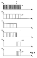
- the signal diagrams illustrated in FIG. 4 to FIG. 7 over the time t serve to supplement one another Explanation of both the inventive method of FIG. 2 as also the inventive circuit arrangement according to FIG. 3.
- the first switching contact N1 as a make contact and the second switching contact N2 acts as a normally closed contact.
- the switching time t0 the switching point of the actuating plunger 8 exceeded becomes.
- the first control signal V1 from low to high level and thus to the first switching contact N1 belonging first driver output Q1 from the open state (low level) in the closed Change state (high level).
- the second control signal V2 from high to low level and thus to the second switching contact N2 belonging second driver output Q2 from the closed Change state (high level) to the open state (low level).
- Fig. 4 shows signal sequences under the assumption that no failures have occurred.
- Watchdog signals Vw dynamically change between the low and the high level.
- the watchdog signals Vw are interrupted, causing the supply driver N3 belonging third driver output Q3 from the high level (almost in Height of the first supply potential Vbb) to the low level (reference potential) drops.
- the second control signal V2 the closing High level has taken, due to the lack of power during the first test intervals .DELTA.t1, the second driver output Q2 briefly Low level on.
- This state transition on the second driver output Q2 stops each Successfully the first test intervals ⁇ t1 with re-occurrence of watchdog signals Vw.
- the first driver output Q1 takes of the opened first switching contact N1 independent of the first test intervals ⁇ t1 the low level.
- the first control signal V1 taken the closing high level. Due to the lack of power supply During the first test intervals ⁇ t1, the first driver output Q1 takes a short time the low level. This state transition at the first driver output Q1 terminates in this case, each time successfully the first test intervals ⁇ t1.
- After the switching time t0 has the second driver output Q2 of the now open second Switching contact N2 regardless of the first test intervals .DELTA.t1 the low level ingested.
- watchdog signals Vw are output again and the switching contacts N1 and N2 via the third driver output Q3 (high level) powered.
- the closing second control signal V2 is set to low, causing the second driver output Q2 to go high the low level drops.
- This state transition at the second driver output Q2 terminates each time successfully the second test intervals ⁇ t2 with renewed reset of the second control signal V2 to the closing signal level (high level).
- the switching time t0 takes the first driver output Q1 regardless of the second test intervals ⁇ t2 the low level.
- the switching time t0 becomes during the second test intervals .DELTA.t2 on the closing first control signal V1 set the low level, causing the first driver output Q1 to the low level drops.
- This state transition at the first driver output Q1 terminates in this Trap each time successfully the second test intervals ⁇ t2 with renewed reset of the first control signal V1 to the closing signal level (high level).
- the second driver output Q2 is independent of the second test intervals ⁇ t2 the low level.
- the third driver output Q3 is switched off from the instant t2 '. slightly delayed time t2 "no more power supply for the switching contacts N1 and N2, whereby the first driver output Q1 forcibly the low level corresponding to the opened state.
- the relevant test interval .DELTA.t2 can not be terminated, and thus the Control signals V1 and V2 no longer take the closing signal level (high level).
- the position switch 2 is also in this case in a waiting state.
- the cause is a defect of the first switching contact N1 containing Output circuit 18 ( Figures 1 and 3) or a defect of the first driver output Q1 to the microcontroller 16 leading back additional amplifier stage 32 ( Figure 3).
- the established contradiction between the first control signal V1 and the signal level of the first driver output Q1 causes from a time t3 'with little, systemic delay compared to the time t3 be exposed to both the watchdog signals Vw and the second Control signal V2 is set to the opening signal level (low level). thereupon all three driver outputs Q1 to Q3 take the low level.
- the position switch 2 is also in a wait state in this case.
Landscapes
- Physics & Mathematics (AREA)
- General Physics & Mathematics (AREA)
- Debugging And Monitoring (AREA)
- Keying Circuit Devices (AREA)
- Rotary Switch, Piano Key Switch, And Lever Switch (AREA)
- Radar Systems Or Details Thereof (AREA)
Abstract
Description
- Figur 1:
- die Blockdarstellung eines nach dem erfindungsgemäßen Verfahren betriebenen elektronisch-mechanischen Positionsschalters;
- Figur 2:
- das Ablaufdiagramm des erfindungsgemäßen Verfahrens;
- Figur 3:
- die Darstellung einer erfindungsgemäßen Schaltungsanordnung;
- Figur 4 -7:
- beispielhafte Signaldiagramme.
- 2
- Positionsschalter
- 4
- Gehäuse
- 6
- Druckfeder
- 8
- Betätigungsstößel
- 10
- Schleifer
- 14
- Stromversorgungsmittel
- 16
- Mikrocontroller
- 18; 19
- Ausgangsschaltung
- 20
- Schaltungsmittel
- 22
- Zeitstufe
- 23
- Differenzierglied
- 24
- Integrierglied
- 26; 28
- Anschlussklemmen
- 30 ... 33
- Verstärkerstufe
- 34; 36
- Außenanschlüsse
- A ... E
- Verfahrensschritte
- Cn
- Kondensatoren
- GND
- Bezugspotential
- H1
- LED-Anzeige
- N1; N2
- Schaltkontakte
- N3
- Versorgungstreiber
- Q1 ... Q3
- Treiberausgang
- R1
- Potentiometer
- Rn
- Widerstände
- S1
- Quittiertaster
- tn; tn'; tn"
- Zeitpunkte
- Tn
- Transistoren
- V1; V2
- Steuersignale
- Va
- Außenspannung
- Vbb; Vdd
- Versorgungspotentiale
- Ve
- Eingangsspannung
- Vr
- Schwellenwert
- Vs
- Schleiferpotential
- Vw
- Watchdog-Signale
- X
- Schleiferposition
- Y
- Betätigungsrichtung
- Z1; Z2
- Z-Dioden
- Δt1; Δt2
- Testintervalle
Claims (11)
- Verfahren zur Funktionsüberwachung eines elektronisch-mechanischen Positionsschalters (2), enthaltend ein Gehäuse (4), einen Betätigungsstößel (8), ein vom diesem beaufschlagtes Potentiometer (R1), einen Mikrocontroller (16), mindestens einen elektronischen Schaltkontakt (N1; N2), Stromversorgungsmittel (14) und Anschlussklemmen (26; 28), wobei durch den Mikrocontroller (16) ein am Schleifer (10) des Potentiometers (R1) anstehendes Schleiferpotential (Vs) erfasst, gegenüber einem gespeicherten Schwellenwert (Vr) bewertet und nach Über- bzw. Unterschreiten des Schwellenwertes (Vr) durch das Schleiferpotential (Vs) der mindestens eine Schaltkontakt (N1; N2) über ein Steuersignal (V1; V2) geschlossen oder geöffnet wird,
gekennzeichnet durch die nacheinander folgenden Verfahrensschritte:A mit ersten Testintervallen (Δt1) werden vom Mikrocontroller (16) ausgegebene, dynamisch wechselnde Watchdog-Signale (Vw) ausgesetzt, worauf Watchdog-Signale überwachende Schaltungsmittel (20) die Stromversorgung des Schaltkontaktes (N1; N2) unterbrechen,B nach dem Zustandsübergang des vom Mikrocontroller (16) überwachten Schaltkontaktes (N1; N2) vom geschlossenen in den geöffneten Zustand werden erneut Watchdog-Signale (Vw) ausgegeben, wogegen bei Ausbleiben des Zustandsüberganges das Steuersignal (V1; V2) zum Öffnen des Schaltkontaktes (N1; N2) gesetzt wird,C innerhalb gegenüber den ersten Testintervallen versetzter, zweiter Testintervalle (Δt2) wird das schließende Steuersignal (V1; V2) zum Öffnen des Schaltkontaktes (N1; N2) umgeschaltet,D nach dem Zustandsübergang des vom Mikrocontroller (16) überwachten Schaltkontaktes (N1; N2) vom geschlossenen in den geöffneten Zustand wird das Steuersignal (V1; V2) zum Schließen des Schaltkontaktes (N1; N2) zurückgeschaltet, wogegen bei ausbleibendem Zustandsübergang die Ausgabe der Watchdog-Signale (Vw) endet. - Verfahren nach vorstehendem Anspruch, gekennzeichnet durch periodisches Auftreten der ersten und der zweiten Testintervalle (Δt1; Δt2).
- Verfahren nach einem der vorstehenden Ansprüche, dadurch gekennzeichnet, dass die ersten und die zweiten Testintervalle (Δt1; Δt2) nach einem Zeitbereich von 500 bis 1200 Programmzyklen des Mikrocontrollers (16) auftreten.
- Verfahren nach einem der vorstehenden Ansprüche, dadurch gekennzeichnet, dass erst nach wiederholtem Ausbleiben des erwarteten Zustandsüberganges während des ersten bzw. zweiten Testintervalls (Δt1; Δt2) das Steuersignal (V1; V2) zum Öffnen des Schaltkontaktes (N1; N2) wechselt.
- Verfahren nach einem der vorstehenden Ansprüche, gekennzeichnet durchE Vergleichen des Schaltzustandes des mindestens einen Schaltkontaktes (N1; N2) mit der logischen Vorgabe durch den Mikrocontroller (16) außerhalb der Testintervalle (Δt1; Δt2) und bei Nichtübereinstimmung Setzen bzw. Halten des Steuersignals (N1; N2) zum Öffnen sowie Beenden der Watchdog-Signale (Vw).
- Verfahren nach einem der vorstehenden Ansprüche, dadurch gekennzeichnet, dass der Mikrocontroller (16) nach Feststellen eines Fehlers ein Fehlermeldesignal ausgibt.
- Schaltungsanordnung zur Funktionsüberwachung eines elektronisch-mechanischen Positionsschalters (2), der ein Gehäuse (4), einen Betätigungsstößel (8), ein vom diesem beaufschlagtes Potentiometer (R1), einen Mikrocontroller (16), mindestens einen elektronischen Schaltkontakt (N1; N2), Stromversorgungsmittel (14) zur Bereitstellung von Versorgungspotentialen (Vbb; Vdd) und Anschlussklemmen (26; 28) enthält, wobei durch den Mikrocontroller (16) ein am Schleifer (10) des Potentiometers (R1) anstehendes Schleiferpotential (Vs) erfasst, gegenüber einem gespeicherten Schwellenwert (Vr) bewertet und je nach Über- oder Unterschreiten des Schwellenwertes (Vr) durch das Schleiferpotential (Vs) der mindestens eine Schaltkontakt (N1; N2) über ein Steuersignal (V1; V2) geschlossen bzw. geöffnet wird, dadurch gekennzeichnet, dassder Mikrocontroller (16) über einen Watchdog-Signalausgang (PTB2) verfügt, über den dynamisch wechselnde Watchdog-Signale (Vw) ausgegeben werden, die mit ersten Testintervallen (Δt1) aussetzen,mit dem Watchdog-Signalausgang (PTB2) eine Zeitstufe (22) verbunden ist, deren Ausgang beim Auftreten von Watchdog-Signalen (Vw) einen ersten Ausgangszustand und im Übrigen einen zweiten Ausgangszustand einnimmt,mit der Zeitstufe (22) ein Versorgungstreiber (N3) verbunden ist, dessen Ausgang (Q3) bei dem ersten Ausgangszustand der Zeitstufe (22) ein zugeführtes Versorgungspotential (Vbb) durchleitet und anderenfalls sperrt,der mindestens eine Schaltkontakt (N1; N2) Bestandteil einer mindestens einen Ausgangsschaltung (18; 19) ist, die vom Ausgang (Q3) des Versorgungstreiber (N3) gespeist wird,der Mikrocontroller (16) über mindestens einen zu der Ausgangsschaltung (18; 19) geführten Steuerausgang (PTB5; PTB3) für das mindestens eine Steuersignal (V1; V2) verfügt, das während des schließenden Signalpegels innerhalb gegenüber den ersten Testintervallen (Δt1) versetzter, zweiter Testintervalle (Δt2) kurzzeitig den öffnenden Signalpegel einnimmt, undder Mikrocontroller (16) über mindestens einen Kontrolleingang (PTB6; PTB4) verfügt, der mit dem Ausgang (Q1; Q2) des mindestens einen Schaltkontaktes (N1; N2) wirkverbunden ist, wobei der Mikrocontroller (16) das am Kontrolleingang (PTB6; PTB4) anstehenden Kontrollsignals in der Weise verarbeitet, dass im ersten Testintervall (Δt1) nach Übergang des Schaltkontaktes (N1; N2) vom geschlossenen in den geöffneten Zustand erneut Watchdog-Signale (Vw) ausgegeben werden, dagegen bei Ausbleiben des Zustandsüberganges das Steuersignal (V1; V2) bleibend in den öffnenden Zustandpegel überführt wird, und im zweiten Testintervall (Δt2) bei ausbleibendem Zustandsübergang des Schaltkontaktes (N1; N2) vom geschlossenen in den geöffneten Zustand in der Folge die Ausgabe der Watchdog-Signale (Vw) unterbleibt.
- Schaltungsanordnung nach vorstehendem Anspruch, dadurch gekennzeichnet, dass die Zeitstufe (22) nachfolgend aus einer eingangsseitig mit ein passiven Differenzierglied (23) versehenen, ersten Verstärkerstufe (30) und aus einer eingangsseitig mit einem passiven Integrierglied (24) versehenen, zweiten (31) Verstärkerstufe besteht.
- Schaltungsanordnung nach einem der beiden vorstehenden Ansprüche, dadurch gekennzeichnet, dass zwischen dem Ausgang (Q1; Q2) des Schaltkontaktes (N1; N2) und dem Kontrolleingang (PTB6; PTB4) eine zusätzliche Verstärkerstufe (32; 33) angeordnet ist.
- Schaltungsanordnung nach vorstehendem Anspruch, dadurch gekennzeichnet, das die zusätzliche Verstärkerstufe (32; 33) mit entstörenden Schaltungsmitteln (C6; C5) versehen ist.
- Schaltungsanordnung nach einem der Ansprüche 7 bis 10, dadurch gekennzeichnet, dass der Mikrocontroller (16) über einen Meldeausgang (AD1) verfügt, der mit einem optischen Signalelement (H1) verbunden ist und der infolge ausbleibendem Zustandsüberganges des Schaltkontaktes (N1; N2) vom geschlossenen in den geöffneten Zustand während der ersten oder zweiten Testintervalle (Δt1; Δt2) ein Meldesignal abgibt.
Priority Applications (1)
| Application Number | Priority Date | Filing Date | Title |
|---|---|---|---|
| PL04010136T PL1480239T3 (pl) | 2003-05-17 | 2004-04-29 | Sposób i układ do kontroli działania elektroniczno-mechanicznego przełącznika pozycyjnego |
Applications Claiming Priority (2)
| Application Number | Priority Date | Filing Date | Title |
|---|---|---|---|
| DE10322385 | 2003-05-17 | ||
| DE10322385A DE10322385B3 (de) | 2003-05-17 | 2003-05-17 | Verfahren und Schaltungsanordnung zur Funktionsüberwachung eines elektronisch- mechanischen Positionsschalters |
Publications (3)
| Publication Number | Publication Date |
|---|---|
| EP1480239A2 true EP1480239A2 (de) | 2004-11-24 |
| EP1480239A3 EP1480239A3 (de) | 2006-06-07 |
| EP1480239B1 EP1480239B1 (de) | 2010-11-17 |
Family
ID=33039193
Family Applications (1)
| Application Number | Title | Priority Date | Filing Date |
|---|---|---|---|
| EP04010136A Expired - Lifetime EP1480239B1 (de) | 2003-05-17 | 2004-04-29 | Verfahren und Schaltungsanordnung zur Funktionsüberwachung eines elektronisch-mechanischen Positionsschalters |
Country Status (8)
| Country | Link |
|---|---|
| US (1) | US7082023B2 (de) |
| EP (1) | EP1480239B1 (de) |
| AT (1) | ATE488849T1 (de) |
| DE (2) | DE10322385B3 (de) |
| DK (1) | DK1480239T3 (de) |
| ES (1) | ES2357398T3 (de) |
| PL (1) | PL1480239T3 (de) |
| PT (1) | PT1480239E (de) |
Cited By (1)
| Publication number | Priority date | Publication date | Assignee | Title |
|---|---|---|---|---|
| EP1591758A3 (de) * | 2004-04-10 | 2006-04-26 | Moeller GmbH | Verfahren zum Betreiben eines mechanisch-elektronischen Positionsgebers |
Families Citing this family (6)
| Publication number | Priority date | Publication date | Assignee | Title |
|---|---|---|---|---|
| US20060158485A1 (en) * | 2005-01-18 | 2006-07-20 | Hill Gregory S | Power switch system |
| US20080148109A1 (en) * | 2006-12-18 | 2008-06-19 | Bashor Paul D | Implicating multiple possible problematic components within a computer system using indicator light diagnostics |
| DE102016004525A1 (de) * | 2016-04-14 | 2017-10-19 | Andreas Stihl Ag & Co. Kg | Verfahren und Vorrichtung zur Erkennung der Schaltstellung eines Betriebsschalters zur Inbetriebnahme eines Elektromotors |
| CN111263895B (zh) | 2017-10-23 | 2022-02-22 | 阿尔卑斯阿尔派株式会社 | 异常检测装置以及异常检测方法 |
| DE102020205141A1 (de) | 2020-04-23 | 2021-10-28 | Zf Friedrichshafen Ag | Überwachung eines Betriebsartenwahlschalters |
| CN114005400B (zh) * | 2021-10-29 | 2024-02-27 | 昆山国显光电有限公司 | 像素电路和显示面板 |
Family Cites Families (10)
| Publication number | Priority date | Publication date | Assignee | Title |
|---|---|---|---|---|
| GB1307990A (en) * | 1969-05-27 | 1973-02-21 | British Aircraft Corp Ltd | Variable-geometry aircraft |
| BE755715A (fr) | 1969-09-19 | 1971-02-15 | Vaillant Joh Kg | Chauffe-eau a circulation avec dispositif de preparation d'eau de consommation |
| DE3734431C2 (de) * | 1987-10-12 | 1999-03-25 | Mannesmann Vdo Ag | Verfahren und Vorrichtung zur Überwachung des funktionsfähigen Zustands von Endstufenschaltungen für elektromotorische bzw. elektromagnetische Stellglieder |
| US4980793A (en) * | 1988-04-29 | 1990-12-25 | Chrysler Corporation | Open loop control of solenoid coil driver |
| US5184025A (en) * | 1988-11-14 | 1993-02-02 | Elegant Design Solutions, Inc. | Computer-controlled uninterruptible power supply |
| US5218196A (en) * | 1991-09-05 | 1993-06-08 | Frost Controls, Inc. | Light curtain system with system and watchdog microcontrollers |
| US5214560A (en) * | 1992-06-19 | 1993-05-25 | Square D Company | Microprocessor watch-dog monitor for electronic trip units |
| US5621398A (en) * | 1995-08-07 | 1997-04-15 | Saint Switch, Inc. | Programmable switch |
| US6145103A (en) * | 1998-04-07 | 2000-11-07 | Advanced Micro Devices, Inc. | Emulator support mode for disabling and reconfiguring timeouts of a watchdog timer |
| DE20203214U1 (de) * | 2002-02-28 | 2002-06-20 | Moeller GmbH, 53115 Bonn | Elektrisches Schaltgerät |
-
2003
- 2003-05-17 DE DE10322385A patent/DE10322385B3/de not_active Expired - Fee Related
-
2004
- 2004-04-29 PL PL04010136T patent/PL1480239T3/pl unknown
- 2004-04-29 EP EP04010136A patent/EP1480239B1/de not_active Expired - Lifetime
- 2004-04-29 DK DK04010136.2T patent/DK1480239T3/da active
- 2004-04-29 ES ES04010136T patent/ES2357398T3/es not_active Expired - Lifetime
- 2004-04-29 PT PT04010136T patent/PT1480239E/pt unknown
- 2004-04-29 AT AT04010136T patent/ATE488849T1/de active
- 2004-04-29 DE DE502004011890T patent/DE502004011890D1/de not_active Expired - Lifetime
- 2004-05-17 US US10/847,168 patent/US7082023B2/en not_active Expired - Fee Related
Cited By (1)
| Publication number | Priority date | Publication date | Assignee | Title |
|---|---|---|---|---|
| EP1591758A3 (de) * | 2004-04-10 | 2006-04-26 | Moeller GmbH | Verfahren zum Betreiben eines mechanisch-elektronischen Positionsgebers |
Also Published As
| Publication number | Publication date |
|---|---|
| DE10322385B3 (de) | 2004-11-11 |
| US20040228065A1 (en) | 2004-11-18 |
| PL1480239T3 (pl) | 2011-05-31 |
| DE502004011890D1 (de) | 2010-12-30 |
| EP1480239B1 (de) | 2010-11-17 |
| DK1480239T3 (da) | 2011-03-07 |
| EP1480239A3 (de) | 2006-06-07 |
| US7082023B2 (en) | 2006-07-25 |
| PT1480239E (pt) | 2011-01-28 |
| ES2357398T3 (es) | 2011-04-26 |
| ATE488849T1 (de) | 2010-12-15 |
Similar Documents
| Publication | Publication Date | Title |
|---|---|---|
| EP0477309B1 (de) | Vorrichtung zur funktionsüberwachung eines elektrischen verbrauchers, seiner ansteuerung und der dazugehörigen verbindungen | |
| EP0185667B1 (de) | Rücksetzschaltung für mikroprozessoren | |
| EP0870646B1 (de) | Elektronischer Blinkgeber | |
| EP0563787B1 (de) | Überwachungsschaltung für computergesteuerte Sicherheitsgeräte | |
| EP0116701B1 (de) | Diebstahlsicherung | |
| EP1480239B1 (de) | Verfahren und Schaltungsanordnung zur Funktionsüberwachung eines elektronisch-mechanischen Positionsschalters | |
| EP0546244A1 (de) | Schaltungsanordnung für ein Zugfahrzeug | |
| EP0505774B1 (de) | Sicherheitsschaltgerät | |
| DE3623705C2 (de) | ||
| DE1294466B (de) | Elektronische Verzoegerungsschaltung | |
| EP1594021A1 (de) | Schaltungsanordnung sowie Verfahren zum Testen von Relaisschaltkontakten einer digitalen Ausgangsschaltung | |
| DE3722335A1 (de) | Elektronisches, vorzugsweise beruehrungslos arbeitendes schaltgeraet | |
| EP4632399A1 (de) | Bedienvorrichtung mit funktionsüberwachung der schaltzustandsdetektion, zugehörige verwendung und verfahren | |
| DE60017311T2 (de) | Verfahren zur Überwachung der Endstellung eines mobilen Elements und Vorrichtung zur Durchführung des Verfahrens | |
| DE202005012557U1 (de) | Steuerungsvorrichtung und Verstelleinrichtung eines Kraftfahrzeugs | |
| DE3614692C2 (de) | ||
| EP1463076B1 (de) | Verfahren zum Betreiben eines elektronisch-mechanischen Positionsschalters | |
| EP1586863B1 (de) | Mechanisch-elektronischer Positionsgeber | |
| DE19913933A1 (de) | Schaltungsanordnung und Verfahren zum Anschalten eines Verbrauchers | |
| EP0034854B1 (de) | Überwachungsschaltung für eine Signalausgabeschaltung an einer Bremseinrichtung eines Fahrzeuges | |
| EP0660042B1 (de) | Schaltungsanordnung zur Kopplung von spannungsführenden Leitungen mit einem Mikroprozessor | |
| DE10151053B4 (de) | Schaltungsanordnung | |
| DE2549701C2 (de) | Schaltungsanordnung zur Anzeige von Störungen in einer elektrischen Schaltanlage | |
| EP0003755B1 (de) | Schaltungsanordnung zum Empfang von Einfachstrom- und Doppelstrom-Telegrafiezeichen | |
| DE102023102238A1 (de) | Schaltgerät zum elektrischen Ein- und Ausschalten einer mit einer Gleichspannungs-Versorgungseinrichtung verbindbaren elektrischen Last sowie Verfahren zum Betreiben eines solchen Schaltgeräts |
Legal Events
| Date | Code | Title | Description |
|---|---|---|---|
| PUAI | Public reference made under article 153(3) epc to a published international application that has entered the european phase |
Free format text: ORIGINAL CODE: 0009012 |
|
| AK | Designated contracting states |
Kind code of ref document: A2 Designated state(s): AT BE BG CH CY CZ DE DK EE ES FI FR GB GR HU IE IT LI LU MC NL PL PT RO SE SI SK TR |
|
| AX | Request for extension of the european patent |
Extension state: AL HR LT LV MK |
|
| PUAL | Search report despatched |
Free format text: ORIGINAL CODE: 0009013 |
|
| AK | Designated contracting states |
Kind code of ref document: A3 Designated state(s): AT BE BG CH CY CZ DE DK EE ES FI FR GB GR HU IE IT LI LU MC NL PL PT RO SE SI SK TR |
|
| AX | Request for extension of the european patent |
Extension state: AL HR LT LV MK |
|
| 17P | Request for examination filed |
Effective date: 20061127 |
|
| AKX | Designation fees paid |
Designated state(s): AT BE BG CH CY CZ DE DK EE ES FI FR GB GR HU IE IT LI LU MC NL PL PT RO SE SI SK TR |
|
| RAP1 | Party data changed (applicant data changed or rights of an application transferred) |
Owner name: EATON INDUSTIES GMBH |
|
| GRAP | Despatch of communication of intention to grant a patent |
Free format text: ORIGINAL CODE: EPIDOSNIGR1 |
|
| RAP1 | Party data changed (applicant data changed or rights of an application transferred) |
Owner name: EATON INDUSTRIES GMBH |
|
| GRAS | Grant fee paid |
Free format text: ORIGINAL CODE: EPIDOSNIGR3 |
|
| GRAA | (expected) grant |
Free format text: ORIGINAL CODE: 0009210 |
|
| AK | Designated contracting states |
Kind code of ref document: B1 Designated state(s): AT BE BG CH CY CZ DE DK EE ES FI FR GB GR HU IE IT LI LU MC NL PL PT RO SE SI SK TR |
|
| REG | Reference to a national code |
Ref country code: GB Ref legal event code: FG4D Free format text: NOT ENGLISH |
|
| REG | Reference to a national code |
Ref country code: CH Ref legal event code: EP |
|
| REG | Reference to a national code |
Ref country code: IE Ref legal event code: FG4D |
|
| REF | Corresponds to: |
Ref document number: 502004011890 Country of ref document: DE Date of ref document: 20101230 Kind code of ref document: P |
|
| REG | Reference to a national code |
Ref country code: PT Ref legal event code: SC4A Free format text: AVAILABILITY OF NATIONAL TRANSLATION Effective date: 20110121 |
|
| REG | Reference to a national code |
Ref country code: RO Ref legal event code: EPE |
|
| REG | Reference to a national code |
Ref country code: CH Ref legal event code: NV Representative=s name: SERVOPATENT GMBH |
|
| REG | Reference to a national code |
Ref country code: SE Ref legal event code: TRGR |
|
| REG | Reference to a national code |
Ref country code: NL Ref legal event code: T3 |
|
| REG | Reference to a national code |
Ref country code: DK Ref legal event code: T3 |
|
| REG | Reference to a national code |
Ref country code: ES Ref legal event code: FG2A Ref document number: 2357398 Country of ref document: ES Kind code of ref document: T3 Effective date: 20110426 |
|
| PG25 | Lapsed in a contracting state [announced via postgrant information from national office to epo] |
Ref country code: CY Free format text: LAPSE BECAUSE OF FAILURE TO SUBMIT A TRANSLATION OF THE DESCRIPTION OR TO PAY THE FEE WITHIN THE PRESCRIBED TIME-LIMIT Effective date: 20101117 Ref country code: BG Free format text: LAPSE BECAUSE OF FAILURE TO SUBMIT A TRANSLATION OF THE DESCRIPTION OR TO PAY THE FEE WITHIN THE PRESCRIBED TIME-LIMIT Effective date: 20110217 Ref country code: SI Free format text: LAPSE BECAUSE OF FAILURE TO SUBMIT A TRANSLATION OF THE DESCRIPTION OR TO PAY THE FEE WITHIN THE PRESCRIBED TIME-LIMIT Effective date: 20101117 |
|
| PG25 | Lapsed in a contracting state [announced via postgrant information from national office to epo] |
Ref country code: GR Free format text: LAPSE BECAUSE OF FAILURE TO SUBMIT A TRANSLATION OF THE DESCRIPTION OR TO PAY THE FEE WITHIN THE PRESCRIBED TIME-LIMIT Effective date: 20110218 |
|
| PG25 | Lapsed in a contracting state [announced via postgrant information from national office to epo] |
Ref country code: EE Free format text: LAPSE BECAUSE OF FAILURE TO SUBMIT A TRANSLATION OF THE DESCRIPTION OR TO PAY THE FEE WITHIN THE PRESCRIBED TIME-LIMIT Effective date: 20101117 |
|
| PG25 | Lapsed in a contracting state [announced via postgrant information from national office to epo] |
Ref country code: SK Free format text: LAPSE BECAUSE OF FAILURE TO SUBMIT A TRANSLATION OF THE DESCRIPTION OR TO PAY THE FEE WITHIN THE PRESCRIBED TIME-LIMIT Effective date: 20101117 |
|
| PLBE | No opposition filed within time limit |
Free format text: ORIGINAL CODE: 0009261 |
|
| STAA | Information on the status of an ep patent application or granted ep patent |
Free format text: STATUS: NO OPPOSITION FILED WITHIN TIME LIMIT |
|
| REG | Reference to a national code |
Ref country code: HU Ref legal event code: AG4A Ref document number: E010864 Country of ref document: HU |
|
| 26N | No opposition filed |
Effective date: 20110818 |
|
| PG25 | Lapsed in a contracting state [announced via postgrant information from national office to epo] |
Ref country code: MC Free format text: LAPSE BECAUSE OF NON-PAYMENT OF DUE FEES Effective date: 20110430 |
|
| REG | Reference to a national code |
Ref country code: DE Ref legal event code: R097 Ref document number: 502004011890 Country of ref document: DE Effective date: 20110818 |
|
| PGFP | Annual fee paid to national office [announced via postgrant information from national office to epo] |
Ref country code: ES Payment date: 20120426 Year of fee payment: 9 |
|
| PGFP | Annual fee paid to national office [announced via postgrant information from national office to epo] |
Ref country code: AT Payment date: 20120327 Year of fee payment: 9 |
|
| PGFP | Annual fee paid to national office [announced via postgrant information from national office to epo] |
Ref country code: GB Payment date: 20130326 Year of fee payment: 10 Ref country code: RO Payment date: 20130327 Year of fee payment: 10 Ref country code: DK Payment date: 20130325 Year of fee payment: 10 |
|
| PGFP | Annual fee paid to national office [announced via postgrant information from national office to epo] |
Ref country code: LU Payment date: 20130418 Year of fee payment: 10 |
|
| PGFP | Annual fee paid to national office [announced via postgrant information from national office to epo] |
Ref country code: PT Payment date: 20130327 Year of fee payment: 10 |
|
| PGFP | Annual fee paid to national office [announced via postgrant information from national office to epo] |
Ref country code: CZ Payment date: 20130416 Year of fee payment: 10 Ref country code: SE Payment date: 20130405 Year of fee payment: 10 Ref country code: IE Payment date: 20130418 Year of fee payment: 10 Ref country code: CH Payment date: 20130426 Year of fee payment: 10 |
|
| PGFP | Annual fee paid to national office [announced via postgrant information from national office to epo] |
Ref country code: PL Payment date: 20130409 Year of fee payment: 10 Ref country code: HU Payment date: 20130326 Year of fee payment: 10 Ref country code: FI Payment date: 20130405 Year of fee payment: 10 Ref country code: TR Payment date: 20130607 Year of fee payment: 9 |
|
| REG | Reference to a national code |
Ref country code: PT Ref legal event code: MM4A Free format text: LAPSE DUE TO NON-PAYMENT OF FEES Effective date: 20141029 |
|
| REG | Reference to a national code |
Ref country code: DK Ref legal event code: EBP Effective date: 20140430 |
|
| PG25 | Lapsed in a contracting state [announced via postgrant information from national office to epo] |
Ref country code: LU Free format text: LAPSE BECAUSE OF NON-PAYMENT OF DUE FEES Effective date: 20140429 |
|
| REG | Reference to a national code |
Ref country code: CH Ref legal event code: PL |
|
| REG | Reference to a national code |
Ref country code: SE Ref legal event code: EUG |
|
| REG | Reference to a national code |
Ref country code: AT Ref legal event code: MM01 Ref document number: 488849 Country of ref document: AT Kind code of ref document: T Effective date: 20140429 |
|
| GBPC | Gb: european patent ceased through non-payment of renewal fee |
Effective date: 20140429 |
|
| REG | Reference to a national code |
Ref country code: IE Ref legal event code: MM4A |
|
| PG25 | Lapsed in a contracting state [announced via postgrant information from national office to epo] |
Ref country code: PT Free format text: LAPSE BECAUSE OF NON-PAYMENT OF DUE FEES Effective date: 20141029 Ref country code: CZ Free format text: LAPSE BECAUSE OF NON-PAYMENT OF DUE FEES Effective date: 20140429 Ref country code: SE Free format text: LAPSE BECAUSE OF NON-PAYMENT OF DUE FEES Effective date: 20140430 Ref country code: RO Free format text: LAPSE BECAUSE OF NON-PAYMENT OF DUE FEES Effective date: 20140429 Ref country code: LI Free format text: LAPSE BECAUSE OF NON-PAYMENT OF DUE FEES Effective date: 20140430 Ref country code: CH Free format text: LAPSE BECAUSE OF NON-PAYMENT OF DUE FEES Effective date: 20140430 Ref country code: GB Free format text: LAPSE BECAUSE OF NON-PAYMENT OF DUE FEES Effective date: 20140429 Ref country code: FI Free format text: LAPSE BECAUSE OF NON-PAYMENT OF DUE FEES Effective date: 20140429 |
|
| PG25 | Lapsed in a contracting state [announced via postgrant information from national office to epo] |
Ref country code: HU Free format text: LAPSE BECAUSE OF NON-PAYMENT OF DUE FEES Effective date: 20140430 Ref country code: AT Free format text: LAPSE BECAUSE OF NON-PAYMENT OF DUE FEES Effective date: 20140429 |
|
| PG25 | Lapsed in a contracting state [announced via postgrant information from national office to epo] |
Ref country code: IE Free format text: LAPSE BECAUSE OF NON-PAYMENT OF DUE FEES Effective date: 20140429 Ref country code: DK Free format text: LAPSE BECAUSE OF NON-PAYMENT OF DUE FEES Effective date: 20140430 |
|
| REG | Reference to a national code |
Ref country code: ES Ref legal event code: FD2A Effective date: 20150526 |
|
| PG25 | Lapsed in a contracting state [announced via postgrant information from national office to epo] |
Ref country code: ES Free format text: LAPSE BECAUSE OF NON-PAYMENT OF DUE FEES Effective date: 20140430 |
|
| REG | Reference to a national code |
Ref country code: PL Ref legal event code: LAPE |
|
| PG25 | Lapsed in a contracting state [announced via postgrant information from national office to epo] |
Ref country code: PL Free format text: LAPSE BECAUSE OF NON-PAYMENT OF DUE FEES Effective date: 20140429 |
|
| REG | Reference to a national code |
Ref country code: FR Ref legal event code: PLFP Year of fee payment: 13 |
|
| REG | Reference to a national code |
Ref country code: FR Ref legal event code: PLFP Year of fee payment: 14 |
|
| PG25 | Lapsed in a contracting state [announced via postgrant information from national office to epo] |
Ref country code: TR Free format text: LAPSE BECAUSE OF NON-PAYMENT OF DUE FEES Effective date: 20140429 |
|
| REG | Reference to a national code |
Ref country code: FR Ref legal event code: PLFP Year of fee payment: 15 |
|
| PGFP | Annual fee paid to national office [announced via postgrant information from national office to epo] |
Ref country code: BE Payment date: 20180323 Year of fee payment: 15 |
|
| REG | Reference to a national code |
Ref country code: BE Ref legal event code: MM Effective date: 20190430 |
|
| PG25 | Lapsed in a contracting state [announced via postgrant information from national office to epo] |
Ref country code: BE Free format text: LAPSE BECAUSE OF NON-PAYMENT OF DUE FEES Effective date: 20190430 |
|
| PGFP | Annual fee paid to national office [announced via postgrant information from national office to epo] |
Ref country code: FR Payment date: 20230321 Year of fee payment: 20 |
|
| PGFP | Annual fee paid to national office [announced via postgrant information from national office to epo] |
Ref country code: IT Payment date: 20230322 Year of fee payment: 20 |
|
| P01 | Opt-out of the competence of the unified patent court (upc) registered |
Effective date: 20230521 |
|
| PGFP | Annual fee paid to national office [announced via postgrant information from national office to epo] |
Ref country code: NL Payment date: 20230321 Year of fee payment: 20 |
|
| PGFP | Annual fee paid to national office [announced via postgrant information from national office to epo] |
Ref country code: DE Payment date: 20230321 Year of fee payment: 20 |
|
| REG | Reference to a national code |
Ref country code: DE Ref legal event code: R071 Ref document number: 502004011890 Country of ref document: DE |
|
| REG | Reference to a national code |
Ref country code: NL Ref legal event code: MK Effective date: 20240428 |