EP1474828B1 - Gehäuse für ein hochspannungsfestes leistungshalbleitermodul - Google Patents
Gehäuse für ein hochspannungsfestes leistungshalbleitermodul Download PDFInfo
- Publication number
- EP1474828B1 EP1474828B1 EP03701416A EP03701416A EP1474828B1 EP 1474828 B1 EP1474828 B1 EP 1474828B1 EP 03701416 A EP03701416 A EP 03701416A EP 03701416 A EP03701416 A EP 03701416A EP 1474828 B1 EP1474828 B1 EP 1474828B1
- Authority
- EP
- European Patent Office
- Prior art keywords
- power semiconductor
- housing
- electrical lead
- semiconductor module
- gas
- Prior art date
- Legal status (The legal status is an assumption and is not a legal conclusion. Google has not performed a legal analysis and makes no representation as to the accuracy of the status listed.)
- Expired - Lifetime
Links
Images


Classifications
-
- H—ELECTRICITY
- H10—SEMICONDUCTOR DEVICES; ELECTRIC SOLID-STATE DEVICES NOT OTHERWISE PROVIDED FOR
- H10W—GENERIC PACKAGES, INTERCONNECTIONS, CONNECTORS OR OTHER CONSTRUCTIONAL DETAILS OF DEVICES COVERED BY CLASS H10
- H10W76/00—Containers; Fillings or auxiliary members therefor; Seals
- H10W76/10—Containers or parts thereof
- H10W76/12—Containers or parts thereof characterised by their shape
-
- H—ELECTRICITY
- H05—ELECTRIC TECHNIQUES NOT OTHERWISE PROVIDED FOR
- H05K—PRINTED CIRCUITS; CASINGS OR CONSTRUCTIONAL DETAILS OF ELECTRIC APPARATUS; MANUFACTURE OF ASSEMBLAGES OF ELECTRICAL COMPONENTS
- H05K5/00—Casings, cabinets or drawers for electric apparatus
- H05K5/06—Hermetically-sealed casings
-
- H—ELECTRICITY
- H05—ELECTRIC TECHNIQUES NOT OTHERWISE PROVIDED FOR
- H05K—PRINTED CIRCUITS; CASINGS OR CONSTRUCTIONAL DETAILS OF ELECTRIC APPARATUS; MANUFACTURE OF ASSEMBLAGES OF ELECTRICAL COMPONENTS
- H05K7/00—Constructional details common to different types of electric apparatus
- H05K7/14—Mounting supporting structure in casing or on frame or rack
- H05K7/1422—Printed circuit boards receptacles, e.g. stacked structures, electronic circuit modules or box like frames
- H05K7/1427—Housings
- H05K7/1432—Housings specially adapted for power drive units or power converters
- H05K7/14322—Housings specially adapted for power drive units or power converters wherein the control and power circuits of a power converter are arranged within the same casing
-
- H—ELECTRICITY
- H10—SEMICONDUCTOR DEVICES; ELECTRIC SOLID-STATE DEVICES NOT OTHERWISE PROVIDED FOR
- H10W—GENERIC PACKAGES, INTERCONNECTIONS, CONNECTORS OR OTHER CONSTRUCTIONAL DETAILS OF DEVICES COVERED BY CLASS H10
- H10W42/00—Arrangements for protection of devices
- H10W42/80—Arrangements for protection of devices protecting against overcurrent or overload, e.g. fuses or shunts
-
- H—ELECTRICITY
- H10—SEMICONDUCTOR DEVICES; ELECTRIC SOLID-STATE DEVICES NOT OTHERWISE PROVIDED FOR
- H10W—GENERIC PACKAGES, INTERCONNECTIONS, CONNECTORS OR OTHER CONSTRUCTIONAL DETAILS OF DEVICES COVERED BY CLASS H10
- H10W76/00—Containers; Fillings or auxiliary members therefor; Seals
- H10W76/10—Containers or parts thereof
- H10W76/12—Containers or parts thereof characterised by their shape
- H10W76/15—Containers comprising an insulating or insulated base
-
- H—ELECTRICITY
- H10—SEMICONDUCTOR DEVICES; ELECTRIC SOLID-STATE DEVICES NOT OTHERWISE PROVIDED FOR
- H10W—GENERIC PACKAGES, INTERCONNECTIONS, CONNECTORS OR OTHER CONSTRUCTIONAL DETAILS OF DEVICES COVERED BY CLASS H10
- H10W76/00—Containers; Fillings or auxiliary members therefor; Seals
- H10W76/60—Seals
Definitions
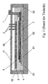
- the invention relates to the field of power electronics. It relates to a power semiconductor module according to the preamble of the independent claim.
- ASIPM application-specific power semiconductor modules
- an ASIPM are one or more power semiconductor devices which take over a switching function, with a control unit in integrated into a module and generally in a common Housing housed.
- the power semiconductor devices For example, these are parallel-connected IGBTs Diode.
- the control unit can, for example, in addition to a Actual control of the power semiconductor components Provide protection functions that, for example, on based on a temperature or current monitoring and at a Exceeding specified limits disable the IGBTs.
- ASIPMs are designed according to similar guidelines like standard power semiconductor modules.
- An essential difference is that at the ASIPM the control unit, which generally applied to a board, as well must be housed in the housing. While this is for low Switching voltages up to about 1200V no special difficulties entails, resulting in increasing switching voltages special requirements from a necessary electrical Isolation between the control unit and the power semiconductor devices and between corresponding supply lines.
- the interior becomes the housing often filled with insulation material.
- a silicone gel which in liquid Mold poured into the case and more or less as needed can be cured strongly.
- the insulation material can thus in the form of a more or less viscous liquid or in solid form.
- the housing is not completely filled with the insulating material, because this is at a thermal expansion of the insulating material due to heating during operation of the ASIPM to a - in the worst case, especially in the case of a short circuit, explosive - cause destruction of the housing would.
- the amount of insulation material is sized that a gas-filled volume inside the case remains free of insulation material.
- JP-A-58 112 354 (FUJI DENKI SEIZO KK) a power semiconductor module of the prior state of the technique.
- a power semiconductor module with the characteristics of the independent Claim solves this problem. Further advantageous embodiments of the invention are in the independent claims specified.
- a means for suppressing leakage currents provided which is in an area between the two Supply lines in a surface of an insulating material is sunken, i. that means in case of a liquid Insulation material is immersed in the insulation material, in Fall of a solid insulation material in a recess in engages the surface, the recess preferably This results in that an initially liquid insulation material, in which the agent dips, is cured.
- a housing wall an electrically insulating molding, which in an area between the two leads into a surface an insulating material is sunk.
- the shape shaped so that they are in a gas filled volume in the Inside the housing, the first and the second supply line from each other shields.
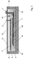
- FIG. 2 schematically shows a power semiconductor module according to the invention.
- a housing which consists of housing walls, i.e. a housing bottom 33, housing sides 32 and a housing cover 31 is formed, which consists of electrically Insulating material is a power semiconductor device 7 with at least a first and a second main contact by means of an electrically conductive layer 62 on a Substrate 61 applied.
- a control unit 8 which has a having electronic circuitry built on a circuit board is and by means of which the power semiconductor device 7 is controllable, is also located inside the Housing.
- a first part of the housing is with an insulating material 4 filled, so that both the power semiconductor device 7 and the control unit 8 from the insulating material 4 are included.
- the gas-filled volume 30 preferably contains air, however, it may also be advantageously filled with an insulating gas be.
- a first electrical lead 1 contacts the electrical conductive layer 62, a second electrical lead 2 the Control unit 8.
- the first electrical lead 1 and the second electrical supply line 2 are both through the gas-filled Volume 30 and the surface 5 is guided in the insulating material 4.
- the housing cover 31 has a molding 34, which in a range between the first electrical supply line 1 and the second electrical lead 2 in the surface is sunken.
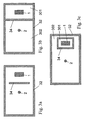
- Fig. 3a shows a section through the power semiconductor module from Fig. 2 along the line A-B. It can be seen that a creepage distance, i. the shortest distance between the first electrical lead 1 and the second electrical Feed line 2 on the surface 5 by the formation 34 in Comparison to a power semiconductor module from the state of Technique in which the formation 34 is not present, clearly is extended.
- a creepage distance i. the shortest distance between the first electrical lead 1 and the second electrical Feed line 2 on the surface 5 by the formation 34 in Comparison to a power semiconductor module from the state of Technique in which the formation 34 is not present, clearly is extended.
- the gas-filled Volume 30 a partial volume 301, through which the first electrical Lead 1 is guided, and in a residual volume 302, through which the second electrical lead 2 is guided.
- a gel is preferably used, preferably a silicone gel or polyurethane.
- silicone electronic potting compounds from Dow Corning (Sylguard 527), Wacker (Silgel), Toshiba et al. These Masses are z.T. are mixed or are made of two components one component.
- Such insulating material 4 may be advantageous introduced in liquid form into the housing, preferably be poured. Depending on the application and viscosity of the Insulation material 4 can leave this in liquid form be, for which, for example, silicone gel is suitable. In this Case dips the formation 34 in the insulation material and is sunk into the surface 5 in this way.
- Insulating material 4 may be necessary Insulating material 4 to harden, resulting from both heating as well as by waiting can be done.
- curing which can be achieved with epoxy advantageous forms by the immersed molding 34 in the surface 5 a correspondingly shaped recess into which the shaping 34 is sunken after curing.
- Oils can also be beneficial be used as insulation material 4. These are due self-healing of its fluid property, i. after one Puncture does not remain a permanent defect in the insulation material 4 exist.
- the molding has 34 preferably has a shape such that it is the first electrical supply line 1 and the second electrical supply line 2 in the gas-filled volume 30 shields against each other. To this Way not only creepage currents are suppressed on the surface 5, but also punctures through the gas-filled volume 30 prevented.
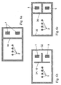
- Fig. 4 shows an advantageous development of an inventive Power semiconductor module according to Fig. 3b or 3c.
- the housing cover 341 has a first opening 35 and a second opening 36, which the partial volume 301 with an exterior connect the housing. This allows refilling a Isolation liquid in the interior of the housing. there serves the first opening 35 for refilling the insulation liquid, while the second opening 36 is an escape of gas made possible from the partial volume 301.
- Fig. 5 shows an alternative embodiment of the invention.
- the Suppression of leakage currents on the surface 5 of the insulating material 4 is in this case by an insulating body 10 is formed, which is sunk into the surface 5.
- a liquid insulating material 4 is a average density of the insulating body 10 to choose suitable, so that it floats on the surface 5, but preferably partially immersed in the insulating material 4.
- an annular insulating body 10 which the first electrical lead 1 or the second electrical lead 2 surrounds.
- the Insulating body 10 can be omitted positioning measures. If the insulating material 4 is cured, must the insulating body 10 optionally during curing be held in a corresponding position.
- Fig. 6 shows further cross sections through advantageous developments a power semiconductor module according to the invention.
- 6a shows a possible example of a power semiconductor module, which a plurality of first electrical leads 1 and has a plurality of second electrical leads 2, wherein the Shaping 34 of the housing cover 31 between the first electrical Supply lines 1 and the second electrical leads 2 is sunk into the surface 5 of the insulating material 4.
- the power semiconductor module in Fig. 6b and 6c has in addition to the first electrical lead 1 and a plurality of second electrical Supply lines 2, a third electrical lead 9.
- the insulating body 10 and the molding 34 of the housing cover 31 is in this case designed to be between all of the first electrical lead 1, the second electrical leads 2 and the third electrical lead 9 formed pairs is sunk into the surface 5.
- the connection advantageous also be applied in such cases in which the first and second electrical supply line (1,2) the first and second main contact of the power semiconductor device 7 contact.
- a control unit 8 but this is not a requirement for the application the invention.
- individual housing walls, in particular, the housing bottom 33 is made electrically conductive be advantageous for example in pressure-contacted power semiconductor modules a contacting of the power semiconductor device 7 make about such a housing wall.
- an insulating body 10 preferably at an electrically be attached to the conductive housing wall and thus an eletrisch form insulating molding 34 of this housing wall.
Landscapes
- Engineering & Computer Science (AREA)
- Microelectronics & Electronic Packaging (AREA)
- Structures Or Materials For Encapsulating Or Coating Semiconductor Devices Or Solid State Devices (AREA)
- Casings For Electric Apparatus (AREA)
Abstract
Description
- 1
- Erste Zuleitung, erste Zuleitungen
- 2
- Zweite Zuleitung, zweite Zuleitungen
- 30
- Gasgefülltes Volumen
- 301
- Teilvolumen
- 302
- Restvolumen
- 31
- Gehäuseabdeckung
- 32
- Gehäuseseitenwand
- 33
- Gehäuseboden
- 34
- Elektrisch isolierende Ausformung
- 35
- Erste Öffnung
- 36
- Zweite Öffnung
- 4
- Isolationsmaterial
- 5
- Oberfläche
- 61
- Substrat
- 62
- Lotschicht
- 7
- Leistungshalbleiterbauelement
- 8
- Kontrolleinheit
- 9
- Dritte Zuleitung
- 10
- Isolationskörper
Claims (8)
- Leistungshalbleitermodul, umfassenddadurch gekennzeichnet, dassein teilweise mit einem Isolationsmaterial (4) gefülltes Gehäuse,ein vom Isolationsmaterial (4) bedecktes Leistungshalbleiterbauelement (7),ein gasgefülltes Volumen (30) in einem Inneren des Gehäuses,eine an das gasgefüllte volumen (30) grenzende Oberfläche (5) des Isolationsmaterials,mindestens eine erste elektrische Zuleitung (1) und eine zweite elektrische Zuleitung (2), welche durch das gasgefüllte Volumen (30) und die Oberfläche (5) in das Isolationamaterial (4) geführt sind,ein Mittel (10) zur Verlängerung oder Eliminierung einer auf der Oberfläche (5) des Isolationsmaterials (4) verlaufenden Kriechstrecke in einem Bereich zwischen der ersten elektrischen Zuleitung (1) und der zweiten elektrischen Zuleitung (2) in diese Oberfläche (5) eingesenkt ist und das Mittel (10) ein Isolationskörper (10) ist.
- Leistungahalbleitermodul, umfassenddadurch gekennzeichnet, dassein teilweise mit einem Isolationsmaterial (4) gefülltes Gehäuse,ein vom Isolationsmaterial (4) bedecktes Leistungshalbleiterbauelement (7),ein gasgefülltes Volumen (30) in einem Inneren des Gehäuses,eine an das gasgefüllte Volumen (30) grenzende Oberfläche (5) des Isolationsmaterials,mindestens eine erste elektrische Zuleitung (1) und eine zweite elektrische Zuleitung (2), welche durch das gasgefüllte Volumen (30) und die Oberfläche (5) in das Isolationsmaterial (4) geführt sind,ein Mittel (34) zur Verlängerung oder Eliminierung einer auf der Oberfläche (5) des Isolationsmaterials (4) verlaufenden Kriechstrecke in einem Bereich zwischen der ersten elektrischen Zuleitung (1) und der zweiten elektrischen Zuleitung (2) in diese Oberfläche (5) eingesenkt ist und das Mittel (34) eine elektrisch isolierende Ausformung (34) einer Gehäusewand (31, 32, 33) ist,die Ausformung (34) die erste elektrische Zuleitung (1) und die zweite elektrische Zuleitung (2) im gasgefüllten Volumen (30) gegeneinander abschirmt.
- Leistungshalbleitermodul nach Anspruch 1 oder 2,
dadurch gekennzeichnet, dassdas Leistungshalbleitermodul mindestens eine Kontrolleinheit (8) enthält, mittels welcher das Leistungshalbleiterbauelement (7) ansteuerbar ist. - Leistungshalbleitermodul nach Anspruch 3, dadurch gekennzeichnet, dassdie Kontrolleinheit (8) vom Isolationsmaterial (4) umgeben ist.
- Leistungshalbleitermodul nach Anspruch 3 oder 4, dadurch gekennzeichnet, dassdas Leistungshalbleiterbauelement mindestens einen Hauptkontakt aufweist,die erste elektrische Zuleitung (1) den mindestens einen Hauptkontakt des Leistungshalbleiterbauelements (7) kontaktiert und dassdie zweite elektrische Zuleitung (2) die Kontrolleinheit (8) kontaktiert.
- Leistungshalbleitermodul nach Anspruch 2, dadurch gekennzeichnet, dassdie Ausformung (34) der Gehäusewand (31, 32, 33) ein Teilvolumen (301) des gasgefüllten Volumens (30), durch welches Teilvolumen (301) die erste elektrische Zuleitung (1) geführt ist, von einem Restvolumen (302), durch welches die zweite elektrische Zuleitung (2) geführt ist, abtrennt.
- Leistungshalbleitermodul nach Anspruch 6, dadurch gekennzeichnet, dassdie Gehäusewand (31, 32, 33) eine erste und eine zweite Öffnung (35,35) aufweist, welche das Teilvolumen (301) mit einem Äueseren des Gehäuses verbinden.
- Leistungshalbleitermodul nach Anspruch 7, dadurch gekennzeichnet, dassdie Ausformung der Gehäusewand (34) die erste oder zweite elektrische Zuleitung (1,2) röhrenförmig umschliesst.
Priority Applications (1)
| Application Number | Priority Date | Filing Date | Title |
|---|---|---|---|
| EP03701416A EP1474828B1 (de) | 2002-02-14 | 2003-02-13 | Gehäuse für ein hochspannungsfestes leistungshalbleitermodul |
Applications Claiming Priority (4)
| Application Number | Priority Date | Filing Date | Title |
|---|---|---|---|
| EP02405110A EP1336990A1 (de) | 2002-02-14 | 2002-02-14 | Gehäuse für ein hochspannungsfestes Leistungshalbleitermodul |
| EP02405110 | 2002-02-14 | ||
| EP03701416A EP1474828B1 (de) | 2002-02-14 | 2003-02-13 | Gehäuse für ein hochspannungsfestes leistungshalbleitermodul |
| PCT/CH2003/000103 WO2003069968A2 (de) | 2002-02-14 | 2003-02-13 | Gehäuse für ein hochspannungsfestes leistungshalbleitermodul |
Publications (2)
| Publication Number | Publication Date |
|---|---|
| EP1474828A2 EP1474828A2 (de) | 2004-11-10 |
| EP1474828B1 true EP1474828B1 (de) | 2005-05-25 |
Family
ID=27619202
Family Applications (2)
| Application Number | Title | Priority Date | Filing Date |
|---|---|---|---|
| EP02405110A Withdrawn EP1336990A1 (de) | 2002-02-14 | 2002-02-14 | Gehäuse für ein hochspannungsfestes Leistungshalbleitermodul |
| EP03701416A Expired - Lifetime EP1474828B1 (de) | 2002-02-14 | 2003-02-13 | Gehäuse für ein hochspannungsfestes leistungshalbleitermodul |
Family Applications Before (1)
| Application Number | Title | Priority Date | Filing Date |
|---|---|---|---|
| EP02405110A Withdrawn EP1336990A1 (de) | 2002-02-14 | 2002-02-14 | Gehäuse für ein hochspannungsfestes Leistungshalbleitermodul |
Country Status (5)
| Country | Link |
|---|---|
| EP (2) | EP1336990A1 (de) |
| JP (1) | JP4652692B2 (de) |
| AU (1) | AU2003203111A1 (de) |
| DE (1) | DE50300583D1 (de) |
| WO (1) | WO2003069968A2 (de) |
Families Citing this family (3)
| Publication number | Priority date | Publication date | Assignee | Title |
|---|---|---|---|---|
| DE102005046063B3 (de) | 2005-09-27 | 2007-03-15 | Semikron Elektronik Gmbh & Co. Kg | Leistungshalbleitermodul mit Überstromschutzeinrichtung |
| ES2367036T3 (es) * | 2005-09-27 | 2011-10-27 | SEMIKRON ELEKTRONIK GMBH & CO. KG PATENTABTEILUNG | Módulo de semiconductor de potencia con medios de protección contra la sobre corriente. |
| DE102009000884B3 (de) * | 2009-02-16 | 2010-10-07 | Semikron Elektronik Gmbh & Co. Kg | Halbleitermodul mit Gehäuse aus präkeramischem Polymer |
Family Cites Families (6)
| Publication number | Priority date | Publication date | Assignee | Title |
|---|---|---|---|---|
| JPS58112354A (ja) * | 1981-12-25 | 1983-07-04 | Fuji Electric Co Ltd | サイリスタ用接続導体 |
| DE3621994A1 (de) * | 1986-07-01 | 1988-01-14 | Bbc Brown Boveri & Cie | Leistungshalbleitermodul |
| DE4418426B4 (de) * | 1993-09-08 | 2007-08-02 | Mitsubishi Denki K.K. | Halbleiterleistungsmodul und Verfahren zur Herstellung des Halbleiterleistungsmoduls |
| JP3222341B2 (ja) * | 1995-01-11 | 2001-10-29 | 株式会社日立製作所 | 半導体モジュール |
| JPH10173098A (ja) * | 1996-12-10 | 1998-06-26 | Mitsubishi Electric Corp | パワー半導体装置およびその製法 |
| JPH1167977A (ja) * | 1997-08-25 | 1999-03-09 | Hitachi Ltd | 樹脂封止型パワーモジュール装置およびその製法 |
-
2002
- 2002-02-14 EP EP02405110A patent/EP1336990A1/de not_active Withdrawn
-
2003
- 2003-02-13 AU AU2003203111A patent/AU2003203111A1/en not_active Abandoned
- 2003-02-13 WO PCT/CH2003/000103 patent/WO2003069968A2/de not_active Ceased
- 2003-02-13 JP JP2003568946A patent/JP4652692B2/ja not_active Expired - Lifetime
- 2003-02-13 DE DE50300583T patent/DE50300583D1/de not_active Expired - Lifetime
- 2003-02-13 EP EP03701416A patent/EP1474828B1/de not_active Expired - Lifetime
Also Published As
| Publication number | Publication date |
|---|---|
| JP4652692B2 (ja) | 2011-03-16 |
| DE50300583D1 (de) | 2005-06-30 |
| AU2003203111A8 (en) | 2003-09-04 |
| AU2003203111A1 (en) | 2003-09-04 |
| JP2005522022A (ja) | 2005-07-21 |
| WO2003069968A2 (de) | 2003-08-21 |
| EP1336990A1 (de) | 2003-08-20 |
| WO2003069968A3 (de) | 2003-11-13 |
| EP1474828A2 (de) | 2004-11-10 |
Similar Documents
| Publication | Publication Date | Title |
|---|---|---|
| DE10221891B4 (de) | Leistungshalbleitervorrichtung | |
| DE2020925C2 (de) | Gehäuse zur Aufnahme von HF-Vierpolen | |
| DE112017002565B4 (de) | Anordnung mit einem elektrischen Bauteil und Verfahren zu deren Herstellung | |
| DE102018126311B4 (de) | Leistungshalbleitermodul | |
| DE10130517C2 (de) | Hochspannungsmodul und Verfahren zu dessen Herstellung | |
| DE4133199C2 (de) | Halbleiterbauelement mit isolationsbeschichtetem Metallsubstrat | |
| EP0750452A1 (de) | Elektronischer Lastschalter für ein Kraftfahrzeug | |
| DE10234477A1 (de) | Leistungshalbleitereinrichtung | |
| DE19906841B4 (de) | Funkenstreckenanordnung und Verfahren zur Herstellung einer vertikalen Funkenstrecke | |
| DE3034902A1 (de) | Impulsunterdruecker | |
| DE102016224232A1 (de) | Leiterplattenvorrichtung | |
| DE3609629A1 (de) | Integrierte elektronische schaltung zum ansteuern von induktiven lasten | |
| EP1336990A1 (de) | Gehäuse für ein hochspannungsfestes Leistungshalbleitermodul | |
| EP0899789A1 (de) | Uberspannungsschutzelement | |
| DE69308910T2 (de) | Selbsttätig geschütztes Halbleiterschutzelement | |
| DE8219553U1 (de) | Halbleitermodul | |
| EP4374425A1 (de) | Anordnung zur kühlung eines hochvoltbauteils | |
| DE10144671A1 (de) | Halbbrücke | |
| DE602004012235T2 (de) | Halbleiterbauelement, halbleiterkörper und verfahren zu seiner herstellung | |
| DE102017109515A1 (de) | Halbleiteranordnung und Verfahren zu deren Herstellung | |
| DE102020124149A1 (de) | Leistungsmodul | |
| DE19903522B4 (de) | Anordnung zur niederinduktiven Führung hoher Ströme insbesondere für einen Stromrichter oder dergleichen | |
| DE102019135271A1 (de) | Leistungsmodul, Stromrichter und Kraftfahrzeugkomponente | |
| DE10122837B4 (de) | Leistungshalbleiter-Modul | |
| DE10332579A1 (de) | Leiterplatte |
Legal Events
| Date | Code | Title | Description |
|---|---|---|---|
| PUAI | Public reference made under article 153(3) epc to a published international application that has entered the european phase |
Free format text: ORIGINAL CODE: 0009012 |
|
| 17P | Request for examination filed |
Effective date: 20040607 |
|
| AK | Designated contracting states |
Kind code of ref document: A2 Designated state(s): AT BE BG CH CY CZ DE DK EE ES FI FR GB GR HU IE IT LI LU MC NL PT SE SI SK TR |
|
| AX | Request for extension of the european patent |
Extension state: AL LT LV MK RO |
|
| GRAP | Despatch of communication of intention to grant a patent |
Free format text: ORIGINAL CODE: EPIDOSNIGR1 |
|
| GRAS | Grant fee paid |
Free format text: ORIGINAL CODE: EPIDOSNIGR3 |
|
| GRAA | (expected) grant |
Free format text: ORIGINAL CODE: 0009210 |
|
| AK | Designated contracting states |
Kind code of ref document: B1 Designated state(s): DE GB |
|
| RBV | Designated contracting states (corrected) |
Designated state(s): DE GB |
|
| REG | Reference to a national code |
Ref country code: GB Ref legal event code: FG4D Free format text: NOT ENGLISH |
|
| REG | Reference to a national code |
Ref country code: IE Ref legal event code: FG4D Free format text: LANGUAGE OF EP DOCUMENT: GERMAN |
|
| REF | Corresponds to: |
Ref document number: 50300583 Country of ref document: DE Date of ref document: 20050630 Kind code of ref document: P |
|
| GBT | Gb: translation of ep patent filed (gb section 77(6)(a)/1977) |
Effective date: 20050917 |
|
| PLBE | No opposition filed within time limit |
Free format text: ORIGINAL CODE: 0009261 |
|
| STAA | Information on the status of an ep patent application or granted ep patent |
Free format text: STATUS: NO OPPOSITION FILED WITHIN TIME LIMIT |
|
| 26N | No opposition filed |
Effective date: 20060228 |
|
| REG | Reference to a national code |
Ref country code: DE Ref legal event code: R081 Ref document number: 50300583 Country of ref document: DE Owner name: HITACHI ENERGY SWITZERLAND AG, CH Free format text: FORMER OWNER: ABB RESEARCH LTD., ZUERICH, CH Ref country code: DE Ref legal event code: R082 Ref document number: 50300583 Country of ref document: DE Representative=s name: DENNEMEYER & ASSOCIATES S.A., DE Ref country code: DE Ref legal event code: R082 Ref document number: 50300583 Country of ref document: DE Representative=s name: ZIMMERMANN & PARTNER PATENTANWAELTE MBB, DE Ref country code: DE Ref legal event code: R081 Ref document number: 50300583 Country of ref document: DE Owner name: ABB POWER GRIDS SWITZERLAND AG, CH Free format text: FORMER OWNER: ABB RESEARCH LTD., ZUERICH, CH Ref country code: DE Ref legal event code: R081 Ref document number: 50300583 Country of ref document: DE Owner name: ABB SCHWEIZ AG, CH Free format text: FORMER OWNER: ABB RESEARCH LTD., ZUERICH, CH |
|
| REG | Reference to a national code |
Ref country code: GB Ref legal event code: 732E Free format text: REGISTERED BETWEEN 20200206 AND 20200212 |
|
| REG | Reference to a national code |
Ref country code: DE Ref legal event code: R081 Ref document number: 50300583 Country of ref document: DE Owner name: HITACHI ENERGY SWITZERLAND AG, CH Free format text: FORMER OWNER: ABB SCHWEIZ AG, BADEN, CH Ref country code: DE Ref legal event code: R082 Ref document number: 50300583 Country of ref document: DE Representative=s name: DENNEMEYER & ASSOCIATES S.A., DE Ref country code: DE Ref legal event code: R081 Ref document number: 50300583 Country of ref document: DE Owner name: ABB POWER GRIDS SWITZERLAND AG, CH Free format text: FORMER OWNER: ABB SCHWEIZ AG, BADEN, CH |
|
| REG | Reference to a national code |
Ref country code: GB Ref legal event code: 732E Free format text: REGISTERED BETWEEN 20210826 AND 20210901 |
|
| PGFP | Annual fee paid to national office [announced via postgrant information from national office to epo] |
Ref country code: GB Payment date: 20220223 Year of fee payment: 20 Ref country code: DE Payment date: 20220217 Year of fee payment: 20 |
|
| REG | Reference to a national code |
Ref country code: DE Ref legal event code: R081 Ref document number: 50300583 Country of ref document: DE Owner name: HITACHI ENERGY SWITZERLAND AG, CH Free format text: FORMER OWNER: ABB POWER GRIDS SWITZERLAND AG, BADEN, CH |
|
| REG | Reference to a national code |
Ref country code: DE Ref legal event code: R071 Ref document number: 50300583 Country of ref document: DE |
|
| REG | Reference to a national code |
Ref country code: GB Ref legal event code: PE20 Expiry date: 20230212 |
|
| PG25 | Lapsed in a contracting state [announced via postgrant information from national office to epo] |
Ref country code: GB Free format text: LAPSE BECAUSE OF EXPIRATION OF PROTECTION Effective date: 20230212 |