EP1467407A1 - Leistungshalbleitermodul - Google Patents
Leistungshalbleitermodul Download PDFInfo
- Publication number
- EP1467407A1 EP1467407A1 EP04006022A EP04006022A EP1467407A1 EP 1467407 A1 EP1467407 A1 EP 1467407A1 EP 04006022 A EP04006022 A EP 04006022A EP 04006022 A EP04006022 A EP 04006022A EP 1467407 A1 EP1467407 A1 EP 1467407A1
- Authority
- EP
- European Patent Office
- Prior art keywords
- power semiconductor
- semiconductor module
- circuit board
- contact
- cover
- Prior art date
- Legal status (The legal status is an assumption and is not a legal conclusion. Google has not performed a legal analysis and makes no representation as to the accuracy of the status listed.)
- Granted
Links
Images


Classifications
-
- H—ELECTRICITY
- H10—SEMICONDUCTOR DEVICES; ELECTRIC SOLID-STATE DEVICES NOT OTHERWISE PROVIDED FOR
- H10W—GENERIC PACKAGES, INTERCONNECTIONS, CONNECTORS OR OTHER CONSTRUCTIONAL DETAILS OF DEVICES COVERED BY CLASS H10
- H10W40/00—Arrangements for thermal protection or thermal control
- H10W40/20—Arrangements for cooling
- H10W40/25—Arrangements for cooling characterised by their materials
- H10W40/255—Arrangements for cooling characterised by their materials having a laminate or multilayered structure, e.g. direct bond copper [DBC] ceramic substrates
-
- H—ELECTRICITY
- H10—SEMICONDUCTOR DEVICES; ELECTRIC SOLID-STATE DEVICES NOT OTHERWISE PROVIDED FOR
- H10W—GENERIC PACKAGES, INTERCONNECTIONS, CONNECTORS OR OTHER CONSTRUCTIONAL DETAILS OF DEVICES COVERED BY CLASS H10
- H10W72/00—Interconnections or connectors in packages
-
- H—ELECTRICITY
- H10—SEMICONDUCTOR DEVICES; ELECTRIC SOLID-STATE DEVICES NOT OTHERWISE PROVIDED FOR
- H10W—GENERIC PACKAGES, INTERCONNECTIONS, CONNECTORS OR OTHER CONSTRUCTIONAL DETAILS OF DEVICES COVERED BY CLASS H10
- H10W90/00—Package configurations
-
- H—ELECTRICITY
- H05—ELECTRIC TECHNIQUES NOT OTHERWISE PROVIDED FOR
- H05K—PRINTED CIRCUITS; CASINGS OR CONSTRUCTIONAL DETAILS OF ELECTRIC APPARATUS; MANUFACTURE OF ASSEMBLAGES OF ELECTRICAL COMPONENTS
- H05K1/00—Printed circuits
- H05K1/02—Details
- H05K1/14—Structural association of two or more printed circuits
- H05K1/144—Stacked arrangements of planar printed circuit boards
-
- H—ELECTRICITY
- H05—ELECTRIC TECHNIQUES NOT OTHERWISE PROVIDED FOR
- H05K—PRINTED CIRCUITS; CASINGS OR CONSTRUCTIONAL DETAILS OF ELECTRIC APPARATUS; MANUFACTURE OF ASSEMBLAGES OF ELECTRICAL COMPONENTS
- H05K3/00—Apparatus or processes for manufacturing printed circuits
- H05K3/30—Assembling printed circuits with electric components, e.g. with resistors
- H05K3/32—Assembling printed circuits with electric components, e.g. with resistors electrically connecting electric components or wires to printed circuits
- H05K3/325—Assembling printed circuits with electric components, e.g. with resistors electrically connecting electric components or wires to printed circuits by abutting or pinching; Mechanical auxiliary parts therefor
-
- H—ELECTRICITY
- H10—SEMICONDUCTOR DEVICES; ELECTRIC SOLID-STATE DEVICES NOT OTHERWISE PROVIDED FOR
- H10W—GENERIC PACKAGES, INTERCONNECTIONS, CONNECTORS OR OTHER CONSTRUCTIONAL DETAILS OF DEVICES COVERED BY CLASS H10
- H10W72/00—Interconnections or connectors in packages
- H10W72/071—Connecting or disconnecting
- H10W72/075—Connecting or disconnecting of bond wires
-
- H—ELECTRICITY
- H10—SEMICONDUCTOR DEVICES; ELECTRIC SOLID-STATE DEVICES NOT OTHERWISE PROVIDED FOR
- H10W—GENERIC PACKAGES, INTERCONNECTIONS, CONNECTORS OR OTHER CONSTRUCTIONAL DETAILS OF DEVICES COVERED BY CLASS H10
- H10W72/00—Interconnections or connectors in packages
- H10W72/50—Bond wires
- H10W72/531—Shapes of wire connectors
- H10W72/5363—Shapes of wire connectors the connected ends being wedge-shaped
-
- H—ELECTRICITY
- H10—SEMICONDUCTOR DEVICES; ELECTRIC SOLID-STATE DEVICES NOT OTHERWISE PROVIDED FOR
- H10W—GENERIC PACKAGES, INTERCONNECTIONS, CONNECTORS OR OTHER CONSTRUCTIONAL DETAILS OF DEVICES COVERED BY CLASS H10
- H10W72/00—Interconnections or connectors in packages
- H10W72/50—Bond wires
- H10W72/541—Dispositions of bond wires
- H10W72/5445—Dispositions of bond wires being orthogonal to a side surface of the chip, e.g. parallel arrangements
-
- H—ELECTRICITY
- H10—SEMICONDUCTOR DEVICES; ELECTRIC SOLID-STATE DEVICES NOT OTHERWISE PROVIDED FOR
- H10W—GENERIC PACKAGES, INTERCONNECTIONS, CONNECTORS OR OTHER CONSTRUCTIONAL DETAILS OF DEVICES COVERED BY CLASS H10
- H10W72/00—Interconnections or connectors in packages
- H10W72/50—Bond wires
- H10W72/541—Dispositions of bond wires
- H10W72/547—Dispositions of multiple bond wires
- H10W72/5475—Dispositions of multiple bond wires multiple bond wires connected to common bond pads at both ends of the wires
-
- H—ELECTRICITY
- H10—SEMICONDUCTOR DEVICES; ELECTRIC SOLID-STATE DEVICES NOT OTHERWISE PROVIDED FOR
- H10W—GENERIC PACKAGES, INTERCONNECTIONS, CONNECTORS OR OTHER CONSTRUCTIONAL DETAILS OF DEVICES COVERED BY CLASS H10
- H10W72/00—Interconnections or connectors in packages
- H10W72/50—Bond wires
- H10W72/551—Materials of bond wires
-
- H—ELECTRICITY
- H10—SEMICONDUCTOR DEVICES; ELECTRIC SOLID-STATE DEVICES NOT OTHERWISE PROVIDED FOR
- H10W—GENERIC PACKAGES, INTERCONNECTIONS, CONNECTORS OR OTHER CONSTRUCTIONAL DETAILS OF DEVICES COVERED BY CLASS H10
- H10W72/00—Interconnections or connectors in packages
- H10W72/90—Bond pads, in general
- H10W72/951—Materials of bond pads
-
- H—ELECTRICITY
- H10—SEMICONDUCTOR DEVICES; ELECTRIC SOLID-STATE DEVICES NOT OTHERWISE PROVIDED FOR
- H10W—GENERIC PACKAGES, INTERCONNECTIONS, CONNECTORS OR OTHER CONSTRUCTIONAL DETAILS OF DEVICES COVERED BY CLASS H10
- H10W74/00—Encapsulations, e.g. protective coatings
-
- H—ELECTRICITY
- H10—SEMICONDUCTOR DEVICES; ELECTRIC SOLID-STATE DEVICES NOT OTHERWISE PROVIDED FOR
- H10W—GENERIC PACKAGES, INTERCONNECTIONS, CONNECTORS OR OTHER CONSTRUCTIONAL DETAILS OF DEVICES COVERED BY CLASS H10
- H10W90/00—Package configurations
- H10W90/701—Package configurations characterised by the relative positions of pads or connectors relative to package parts
- H10W90/751—Package configurations characterised by the relative positions of pads or connectors relative to package parts of bond wires
- H10W90/754—Package configurations characterised by the relative positions of pads or connectors relative to package parts of bond wires between a chip and a stacked insulating package substrate, interposer or RDL
Definitions
- the invention describes a power semiconductor module consisting of a housing Base plate or for direct mounting on a heat sink and at least one in it arranged electrically insulating substrate.
- This in turn consists of one Isolierstoff emotions with a plurality of mutually insulated metallic thereon Connecting tracks and on these and with these connecting tracks Power semiconductor components connected according to the circuit.
- the substrate has a flat metallic layer on its underside, comparable to the Connecting tracks, on.
- such power semiconductor modules have Connection elements for load and auxiliary contacts.
- Power semiconductor modules that are the starting point of this invention are exemplary known from DE 42 37 632 A1 and DE 196 30 173 C2.
- Such power semiconductor modules have at least partially designed as contact springs connection elements Connection of the connecting tracks of the substrate to external connections.
- This Contact springs are arranged in the power semiconductor module such that they Map the pin assignment inside the substrate to the outer pins.
- Another power semiconductor module is known from DE 100 25 696 A1, which discloses a circuit board arranged perpendicular to the substrate. This circuit board is with a partial area inside and with a further partial area outside the Power semiconductor module arranged and thus forms its connection elements.
- the disadvantage here is that due to the position of the circuit board, the outer Pin assignment is determined.
- the present invention is therefore based on the object of a power semiconductor module to be presented in which the internal pin assignment is circuit-compatible and through simple measures to a different external pin assignment can be customized.
- the basic idea of the invention is based on a power semiconductor module with a Base plate or for direct mounting on a heat sink according to the stated status the technology consisting of a frame-like housing with at least one therein arranged electrically insulating substrate.
- This substrate itself consists of an insulating body with a plurality of ones located on its first main surface metallic interconnects insulated from one another and preferably from a flat metallic layer arranged on its second main surface.
- a plurality of power semiconductor components is connected in accordance with the circuit arranged.
- the inventive power semiconductor module points outwards Connection elements for load and auxiliary contacts.
- Connection elements is formed in the interior of the power semiconductor module Contact connector, preferably contact springs, in a holding device between Connection tracks and contact points arranged on a printed circuit board are.
- the printed circuit board has conductor tracks that have these contact points with the outside leading contact elements, which are also arranged on this circuit board, connects.
- the arrangement of further components on the circuit board Functionality of the power semiconductor module can be increased.
- An advantage of this embodiment of a power semiconductor module is that the outer Pin assignment can be selected independently of the inner. So must exemplary driver boards when changing the substrate or substrates and / or the type or the number of power semiconductor components cannot be changed.
- FIG. 1 shows a top view of a power semiconductor module according to the invention.
- a power semiconductor module consisting of a base plate (20) for mounting on a heat sink.
- this base plate (20) has one in the region of its corners Recess (22).
- the module also consists of a frame-like housing (30) and two electrically insulating substrates (50).
- the respective substrate exists in turn from an insulating body (52) with a plurality of on its first one Main surface facing away from the base plate are metallic insulated from each other Connection tracks (54).
- On its second main surface facing the base plate the substrate has a flat surface similar to the connecting tracks of the first main surface Metallization (53, Fig. 2).
- connection tracks (54) and with them are connected in accordance with the circuit by means of wire bond connections (58) Power semiconductor components (56) and a sensor component (58) arranged. to The submodule (10) has electrical contacts for connection elements (40) for the Load connections.
- the connecting tracks (54) of the substrates (50) are in part with each other and with the connection elements (40) by means of wire bond connections (42, 44, 46) connected.
- the power semiconductor component according to the invention has spring contacts (60) on, which are arranged on a subframe, not shown. These spring contacts (60) connect the connecting tracks (54) to contact points on a printed circuit board (71). These contact points are arranged on the underside of the circuit board (71), which continues has conductor tracks (72) on this underside facing the substrate (50). This connect the contact points (78) with contact elements leading to the outside, here Pin connectors (74). Alternatively, solder eyelets or solder pins are exemplary possible contact elements. These contact elements penetrate the cover (70) and set thus represents the external connection assignment. This external connection assignment differs from the represented by the contact points of the spring contacts on the substrate (50) Terminal assignment significantly. Thus, the invention allows Power semiconductor component an outer completely independent of the inner Pin assignment.
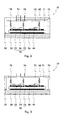
- FIGS. 2 to 5 show different configurations of an inventive Power semiconductor module (10) with a frame-like housing (30) in a side view.
- a so-called DCB (Direct Copper Bonding) substrate (50) is arranged on the base plate (20).
- This Copper layer (54) represents the connecting tracks of the power semiconductor module these connecting tracks (54) are the components (56), as a rule Power semiconductor components and sensor components, arranged.
- the circuit-friendly Connections are made using wire bond connections (44).
- connection elements are in the first part of their course by means of contact springs (60) formed between contact points on the connecting tracks (54) and Contact surfaces (78) are arranged on a printed circuit board (71).
- connection elements by connecting tracks (72) on the circuit board (71) and to the outside leading by means of contact pins (74) also arranged on the circuit board Pin connector (76) formed, wherein the contact pins (76) penetrate the cover (70).
- connection elements are also in the first part of their course Contact springs (60) and conductor tracks (72) arranged on a printed circuit board are formed.
- the lid is designed like a frame and encloses the circuit board at its edges without completely covering it.
- the Contact elements (76) for the external contact are made by solder pins, which Penetrate circuit board (71), formed.
- lid (70) itself designed as a printed circuit board by directly connecting conductor tracks on its inside are arranged. Such methods are exemplified as MID (Molded Interconnect Devices).
- the contact elements (76) are here in the plastic of the cover (70) injected solder pins.
- FIG. 5 shows an experience-based power semiconductor module according to FIG. 3 with a increased functionality.
- further active and / or passive Components such as resistors, capacitors or integrated circuits, are made the well-known power semiconductor module an intelligent power semiconductor module, because here at least partially the functionality of a driver or other circuit (evaluation, Sensor circuit) is arranged directly in or on the module. If so Load connections are designed in the manner described, current sensors and whose evaluation circuits are arranged on the circuit board.
- Fig. 5 also shows an additional contact connector, a contact spring (60), the Base plate (60) and thus also the heat sink in an electrically conductive manner with the printed circuit board (71) combines. This potential is thus exemplified on the printed circuit board (71) arranged evaluation circuits provided.
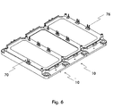
- FIG. 6 shows an arrangement of three power semiconductor modules according to the invention in three-dimensional view.
- three power semiconductor modules (10) each form a half-bridge circuit a 3-phase bridge circuit.
- a common lid (70) with an arrangement of the conductor tracks (72) and contact elements (76) according to FIG. 5 covers all three individual modules (10).
Landscapes
- Cooling Or The Like Of Semiconductors Or Solid State Devices (AREA)
- Inverter Devices (AREA)
- Bipolar Transistors (AREA)
- Combinations Of Printed Boards (AREA)
- Coupling Device And Connection With Printed Circuit (AREA)
Abstract
Description
- Fig. 1
- zeigt ein Teilmodul eines erfindungsgemäßen Leistungshalbleitermoduls in Draufsicht.
- Fig 2
- zeigt eine Ausgestaltung eines erfindungsgemäßen Leistungshalbleitermoduls in Seitenansicht.
- Fig. 3
- zeigt eine weitere Ausgestaltung eines erfindungsgemäßen Leistungshalbleitermoduls in Seitenansicht.
- Fig. 4
- zeigt eine weitere Ausgestaltung eines erfindungsgemäßen Leistungshalbleitermoduls in Seitenansicht.
- Fig. 5
- zeigt eine erfindungsgemäße Ausgestaltung eines intelligenten Leistungshalbleitermoduls in Seitenansicht.
- Fig. 6
- zeigt eine Anordnung von drei erfindungsgemäßen Leistungshalbleitermodulen in dreidimensionaler Ansicht.
Claims (9)
- Leistungshalbleitermodul (10) mit einer Grundplatte (20) oder zur direkten Montage auf einem Kühlkörper bestehend aus einem rahmenartigen Gehäuse (30) einem Deckel (70) und mit mindestens einem innerhalb des Gehäuses (30) angeordneten elektrisch isolierenden Substrat (50), das seinerseits besteht aus einem Isolierstoffkörper (52) mit einer Mehrzahl von darauf befindlichen gegeneinander isolierten metallischen Verbindungsbahnen (54), darauf befindlichen und mit diesen Verbindungsbahnen schaltungsgerecht verbundenen Leistungshalbleiterbauelementen (56) sowie nach außen führenden Anschlusselementen für Last- und Hilfskontakte, wobei zumindest ein Teil der Anschlusselemente im Inneren des Leistungshalbleitermoduls gebildet wird durch Kontaktverbinder (60), die zwischen Verbindungsbahnen (54) und Kontaktpunkten (78) auf einer Leiterplatte (71) angeordnet sind und wobei diese Leiterplatte Leiterbahnen (72) aufweist, die diese Kontaktpunkte mit nach außen führenden Kontaktelementen (76) verbindet.
- Leistungshalbleitermodul (10) nach Anspruch 1, wobei
auf der Leiterplatte (71) aktive und / oder passive elektronische Bauelemente (80, 82) angeordnet und schaltungsgerecht mit den Verbindungsbahnen (72) verbunden sind. - Leistungshalbleitermodul nach Anspruch 1 oder 2, wobei
auch die Grundplatte (20) oder der Kühlkörper mittels mindestens eines Kontaktverbinders (60) mit der Leiterplatte (71) verbunden ist. - Leistungshalbleitermodul nach Anspruch 1 oder 2, wobei
die Kontaktverbinder (60) als Kontaktfedern ausgebildet sind. - Leistungshalbleitermodul nach Anspruch 1 oder 2, wobei
die Leiterplatte (71) innerhalb des Leistungshalbleitermoduls (1) parallel zwischen dem Substrat (50) und dem Deckel (70) angeordnet ist und diese Leiterplatte (71) Kontaktelemente (76) aufweist, die durch die Leiterplatte selbst sowie den Deckel hindurch führen. - Leistungshalbleitermodul nach Anspruch 1 oder 2, wobei
die Leiterplatte (71) innerhalb eines rahmenartig ausgebildeten Deckels (70) eingebettet ist und somit selbst einen Teil des Deckels (70) bildet. - Leistungshalbleitermodul nach Anspruch 1 oder 2, wobei
die Leiterplatte gebildet wird aus dem Deckel (70) selbst mit, auf seiner Innenseite angeordneten Leiterbahnen und wobei das Leistungshalbleitermodul durch diesen Deckel hindurchführende Kontaktelemente (76) aufweist. - Leistungshalbleitermodul nach Anspruch 1 oder 2, wobei
die Kontaktelemente als Steckstiftverbinder oder Lötösen ausgebildet sind. - Leistungshalbleitermodul nach Anspruch 1 oder 2, wobei
mindestens ein Substrat (50) ein Sensorikbauteil aufweist.
Applications Claiming Priority (2)
| Application Number | Priority Date | Filing Date | Title |
|---|---|---|---|
| DE10316355 | 2003-04-10 | ||
| DE10316355A DE10316355C5 (de) | 2003-04-10 | 2003-04-10 | Leistungshalbeitermodul mit flexibler äusserer Anschlussbelegung |
Publications (2)
| Publication Number | Publication Date |
|---|---|
| EP1467407A1 true EP1467407A1 (de) | 2004-10-13 |
| EP1467407B1 EP1467407B1 (de) | 2008-12-03 |
Family
ID=32404459
Family Applications (1)
| Application Number | Title | Priority Date | Filing Date |
|---|---|---|---|
| EP04006022A Expired - Lifetime EP1467407B1 (de) | 2003-04-10 | 2004-03-13 | Leistungshalbleitermodul |
Country Status (7)
| Country | Link |
|---|---|
| US (1) | US6958534B2 (de) |
| EP (1) | EP1467407B1 (de) |
| JP (1) | JP4264375B2 (de) |
| AT (1) | ATE416478T1 (de) |
| DE (2) | DE10316355C5 (de) |
| DK (1) | DK1467407T3 (de) |
| ES (1) | ES2316889T3 (de) |
Families Citing this family (42)
| Publication number | Priority date | Publication date | Assignee | Title |
|---|---|---|---|---|
| DE10333328B3 (de) * | 2003-07-23 | 2005-01-27 | Semikron Elektronik Gmbh | Leistungshalbleitermodul in skalierbarer Aufbautechnik |
| DE10333329B4 (de) | 2003-07-23 | 2011-07-21 | SEMIKRON Elektronik GmbH & Co. KG, 90431 | Leistungshalbleitermodul mit biegesteifer Grundplatte |
| DE102004025609B4 (de) * | 2004-05-25 | 2010-12-09 | Semikron Elektronik Gmbh & Co. Kg | Anordnung in Schraub- Druckkontaktierung mit einem Leistungshalbleitermodul |
| DE102005024900B4 (de) * | 2004-06-08 | 2012-08-16 | Fuji Electric Co., Ltd. | Leistungsmodul |
| FR2877436B1 (fr) * | 2004-11-03 | 2007-01-26 | Mitsubishi Electric Corp | Dispositif de detection de courant |
| DE102004057421B4 (de) * | 2004-11-27 | 2009-07-09 | Semikron Elektronik Gmbh & Co. Kg | Druckkontaktiertes Leistungshalbleitermodul für hohe Umgebungstemperaturen und Verfahren zu seiner Herstellung |
| DE102004061099B4 (de) * | 2004-12-18 | 2010-11-11 | Semikron Elektronik Gmbh & Co. Kg | Verfahren zur Herstellung eines Leistungshalbleitermoduls mit ESD-Schutzbeschaltung |
| DE102005063532B3 (de) | 2005-02-17 | 2022-03-10 | Infineon Technologies Ag | Leistungshalbleiterbaugruppe |
| DE102005046063B3 (de) * | 2005-09-27 | 2007-03-15 | Semikron Elektronik Gmbh & Co. Kg | Leistungshalbleitermodul mit Überstromschutzeinrichtung |
| ES2367036T3 (es) * | 2005-09-27 | 2011-10-27 | SEMIKRON ELEKTRONIK GMBH & CO. KG PATENTABTEILUNG | Módulo de semiconductor de potencia con medios de protección contra la sobre corriente. |
| DE102005053396B4 (de) * | 2005-11-09 | 2010-04-15 | Semikron Elektronik Gmbh & Co. Kg | Schaltungseinrichtung, insbesondere Frequenzumrichter |
| DE102005055713B4 (de) * | 2005-11-23 | 2011-11-17 | Semikron Elektronik Gmbh & Co. Kg | Leistungshalbleitermodul mit Anschlusselementen |
| DE102006008807B4 (de) * | 2006-02-25 | 2010-10-14 | Semikron Elektronik Gmbh & Co. Kg | Anordnung mit einem Leistungshalbleitermodul und einem Kühlbauteil |
| DE102006011995B3 (de) * | 2006-03-16 | 2007-11-08 | Semikron Elektronik Gmbh & Co. Kg | Leistungshalbleitermodul mit segmentierter Grundplatte |
| DE102006021412B3 (de) * | 2006-05-09 | 2007-11-15 | Semikron Elektronik Gmbh & Co. Kg | Leistungshalbleitermodul |
| DE102006025453B4 (de) * | 2006-05-31 | 2009-12-24 | Infineon Technologies Ag | Halbleiterschaltungsanordnung |
| DE102006027481C5 (de) * | 2006-06-14 | 2012-11-08 | Semikron Elektronik Gmbh & Co. Kg | Leistungshalbleitermodul mit gegeneinander elektrisch isolierten Anschlusselementen |
| DE102007022336A1 (de) * | 2007-05-12 | 2008-11-20 | Semikron Elektronik Gmbh & Co. Kg | Leistungshalbleitersubstrat mit Metallkontaktschicht sowie Herstellungsverfahren hierzu |
| WO2009023551A1 (en) * | 2007-08-10 | 2009-02-19 | Arizona Board Of Regents And On Behalf Of Arizona State University | Hybrid integrated mems reconfigurable antenna array (himra) |
| JP5176507B2 (ja) * | 2007-12-04 | 2013-04-03 | 富士電機株式会社 | 半導体装置 |
| DE102008018841A1 (de) * | 2008-04-15 | 2009-10-22 | Conti Temic Microelectronic Gmbh | Verfahren zur Herstellung und Aufbau eines Leistungsmoduls |
| EP2549534B1 (de) * | 2010-03-16 | 2019-07-03 | Fuji Electric Co., Ltd. | Halbleiterbauelement |
| DE102010053392A1 (de) | 2010-12-03 | 2012-06-06 | Volkswagen Ag | Leistungshalbleitermodul, Kondensatormodul, Schaltungsanordnung sowie elektrisches System eines Kraftfahrzeugs |
| GB201122324D0 (en) | 2011-12-23 | 2012-02-01 | Univ Edinburgh | Antenna element & antenna device comprising such elements |
| DE102012012759A1 (de) * | 2012-06-27 | 2014-01-02 | Sensitec Gmbh | Anordnung zur Strommessung |
| CN104701277B (zh) * | 2013-12-10 | 2017-12-05 | 江苏宏微科技股份有限公司 | 功率模块的封装结构 |
| DE202014003171U1 (de) | 2014-04-15 | 2014-05-14 | Ixys Semiconductor Gmbh | Leistungshalbleitermodul |
| EP2933836B1 (de) | 2014-04-15 | 2020-10-14 | IXYS Semiconductor GmbH | Leistungshalbleitermodul |
| US10959342B2 (en) | 2019-04-08 | 2021-03-23 | Kevin R. Williams | Condensation resistant power semiconductor module |
| US9620877B2 (en) | 2014-06-17 | 2017-04-11 | Semiconductor Components Industries, Llc | Flexible press fit pins for semiconductor packages and related methods |
| DE102014109816B4 (de) * | 2014-07-14 | 2016-11-03 | Infineon Technologies Ag | Leistungshalbleitermodul und System mit mindestens zwei Leistungshalbleitermodulen |
| DE102014110008A1 (de) * | 2014-07-16 | 2016-01-21 | Infineon Technologies Ag | Träger, Halbleitermodul und Verfahren zu deren Herstellung |
| CN105336723B (zh) * | 2014-07-28 | 2018-09-14 | 通用电气公司 | 半导体模块、半导体模块组件及半导体装置 |
| US9431311B1 (en) | 2015-02-19 | 2016-08-30 | Semiconductor Components Industries, Llc | Semiconductor package with elastic coupler and related methods |
| DE102016107083B4 (de) * | 2016-04-18 | 2019-05-23 | Semikron Elektronik Gmbh & Co. Kg | Leistungselektronische Anordnung und Fahrzeug hiermit |
| DE202016006849U1 (de) * | 2016-11-07 | 2018-02-08 | Liebherr-Elektronik Gmbh | Leistungselektronikmodul |
| CN111162015A (zh) * | 2019-12-20 | 2020-05-15 | 珠海格力电器股份有限公司 | 一种智能功率模块及封装方法 |
| EP3937214A1 (de) * | 2020-07-07 | 2022-01-12 | Siemens Aktiengesellschaft | Verfahren zur herstellung einer leistungseinheit |
| DE102022213628A1 (de) * | 2022-12-14 | 2024-06-20 | Robert Bosch Gesellschaft mit beschränkter Haftung | Leistungsmodul |
| DE102022213629A1 (de) * | 2022-12-14 | 2024-06-20 | Robert Bosch Gesellschaft mit beschränkter Haftung | Leistungsmodul |
| DE102023116599A1 (de) * | 2023-06-23 | 2024-12-24 | Infineon Technologies Ag | Halbleitermodulanordnung |
| WO2025191977A1 (ja) * | 2024-03-15 | 2025-09-18 | 富士電機株式会社 | パワー半導体装置及びその製造方法 |
Citations (6)
| Publication number | Priority date | Publication date | Assignee | Title |
|---|---|---|---|---|
| US4965710A (en) * | 1989-11-16 | 1990-10-23 | International Rectifier Corporation | Insulated gate bipolar transistor power module |
| EP1032042A2 (de) * | 1999-02-22 | 2000-08-30 | Hitachi, Ltd. | Halbleitermodul, dieses verwendenter Leistungswandler und seine Herstellung |
| US20020070439A1 (en) * | 2000-12-13 | 2002-06-13 | Mitsubishi Denki Kabushiki Kaisha | Semiconductor device |
| US6421244B1 (en) * | 1999-12-28 | 2002-07-16 | Mitsubishi Denki Kabushiki Kaisha | Power module |
| WO2002058152A2 (en) * | 2001-01-17 | 2002-07-25 | Matsushita Electric Industrial Co., Ltd. | Electronic circuit device and method for manufacturing the same |
| EP1289014A1 (de) * | 2001-04-02 | 2003-03-05 | Mitsubishi Denki Kabushiki Kaisha | Leistungshalbleiter |
Family Cites Families (9)
| Publication number | Priority date | Publication date | Assignee | Title |
|---|---|---|---|---|
| DE4237632A1 (de) * | 1992-11-07 | 1994-05-11 | Export Contor Ausenhandelsgese | Schaltungsanordnung |
| DE19630173C2 (de) * | 1996-07-26 | 2001-02-08 | Semikron Elektronik Gmbh | Leistungsmodul mit Halbleiterbauelementen |
| US6414391B1 (en) * | 1998-06-30 | 2002-07-02 | Micron Technology, Inc. | Module assembly for stacked BGA packages with a common bus bar in the assembly |
| IT1308047B1 (it) * | 1999-05-25 | 2001-11-29 | Ohg Accossato Giovanni S A S D | Dispositivo di comando del freno o della frizione di un motociclo eleva di manovra per tale dispositivo |
| JP2001036002A (ja) * | 1999-07-23 | 2001-02-09 | Fuji Electric Co Ltd | 半導体装置 |
| US6222264B1 (en) * | 1999-10-15 | 2001-04-24 | Dell Usa, L.P. | Cooling apparatus for an electronic package |
| DE10101086B4 (de) * | 2000-01-12 | 2007-11-08 | International Rectifier Corp., El Segundo | Leistungs-Moduleinheit |
| US6373125B1 (en) | 2000-02-23 | 2002-04-16 | International Business Machines Corporation | Chip scale package with direct attachment of chip to lead frame |
| US6867493B2 (en) * | 2000-11-15 | 2005-03-15 | Skyworks Solutions, Inc. | Structure and method for fabrication of a leadless multi-die carrier |
-
2003
- 2003-04-10 DE DE10316355A patent/DE10316355C5/de not_active Expired - Fee Related
-
2004
- 2004-03-13 EP EP04006022A patent/EP1467407B1/de not_active Expired - Lifetime
- 2004-03-13 DE DE502004008566T patent/DE502004008566D1/de not_active Expired - Lifetime
- 2004-03-13 DK DK04006022T patent/DK1467407T3/da active
- 2004-03-13 AT AT04006022T patent/ATE416478T1/de not_active IP Right Cessation
- 2004-03-13 ES ES04006022T patent/ES2316889T3/es not_active Expired - Lifetime
- 2004-03-29 JP JP2004095429A patent/JP4264375B2/ja not_active Expired - Fee Related
- 2004-04-09 US US10/821,290 patent/US6958534B2/en not_active Expired - Fee Related
Patent Citations (6)
| Publication number | Priority date | Publication date | Assignee | Title |
|---|---|---|---|---|
| US4965710A (en) * | 1989-11-16 | 1990-10-23 | International Rectifier Corporation | Insulated gate bipolar transistor power module |
| EP1032042A2 (de) * | 1999-02-22 | 2000-08-30 | Hitachi, Ltd. | Halbleitermodul, dieses verwendenter Leistungswandler und seine Herstellung |
| US6421244B1 (en) * | 1999-12-28 | 2002-07-16 | Mitsubishi Denki Kabushiki Kaisha | Power module |
| US20020070439A1 (en) * | 2000-12-13 | 2002-06-13 | Mitsubishi Denki Kabushiki Kaisha | Semiconductor device |
| WO2002058152A2 (en) * | 2001-01-17 | 2002-07-25 | Matsushita Electric Industrial Co., Ltd. | Electronic circuit device and method for manufacturing the same |
| EP1289014A1 (de) * | 2001-04-02 | 2003-03-05 | Mitsubishi Denki Kabushiki Kaisha | Leistungshalbleiter |
Also Published As
| Publication number | Publication date |
|---|---|
| DK1467407T3 (da) | 2009-02-23 |
| ATE416478T1 (de) | 2008-12-15 |
| JP4264375B2 (ja) | 2009-05-13 |
| EP1467407B1 (de) | 2008-12-03 |
| DE502004008566D1 (de) | 2009-01-15 |
| JP2004319991A (ja) | 2004-11-11 |
| DE10316355B3 (de) | 2004-07-01 |
| US6958534B2 (en) | 2005-10-25 |
| DE10316355C5 (de) | 2008-03-06 |
| ES2316889T3 (es) | 2009-04-16 |
| US20040245548A1 (en) | 2004-12-09 |
Similar Documents
| Publication | Publication Date | Title |
|---|---|---|
| DE10316355B3 (de) | Leistungshalbeitermodul mit flexibler äusserer Anschlussbelegung | |
| EP1450404B1 (de) | Anordnung in Druckkontaktierung mit einem Leistungshalbleitermodul | |
| DE19520700B4 (de) | Halbleiterbausteinanordnung | |
| EP0855090B1 (de) | Multichipmodul | |
| DE10201781B4 (de) | Hochfrequenz-Leistungsbauteil und Hochfrequenz-Leistungsmodul sowie Verfahren zur Herstellung derselben | |
| DE10250538A1 (de) | Elektronisches Bauteil als Multichipmodul und Verfahren zu dessen Herstellung | |
| DE102013201931B4 (de) | Laserbauelement und Verfahren zu seiner Herstellung | |
| DE102006034679A1 (de) | Halbleitermodul mit Leistungshalbleiterchip und passiven Bauelement sowie Verfahren zur Herstellung desselben | |
| DE19801312A1 (de) | Halbleiterbauelement mit mehreren Substratlagen und zumindest einem Halbleiterchip und einem Verfahren zum Herstellen eines solchen Halbleiterbauelementes | |
| DE10142119A1 (de) | Elektronisches Bauteil und Verfahren zu seiner Herstellung | |
| EP1192841A1 (de) | Intelligentes leistungsmodul | |
| WO1999000845A1 (de) | Elektronisches steuergerät | |
| DE10333328B3 (de) | Leistungshalbleitermodul in skalierbarer Aufbautechnik | |
| DE102006016345A1 (de) | Halbleitermodul mit diskreten Bauelementen und Verfahren zur Herstellung desselben | |
| DE102009027416B4 (de) | Halbleitermodul mit steckbarem Anschluss und Verfahren zur Herstellung eines Halbleitermoduls mit steckbarem Anschluss | |
| DE19924991A1 (de) | Intelligentes Leistungsmodul in Sandwich-Bauweise | |
| EP2436242B1 (de) | Optoelektronisches modul und verfahren zur herstellung eines optoelektronischen moduls | |
| DE19924994A1 (de) | Intelligentes Leistungsmodul | |
| EP2033219A1 (de) | Leistungsgehäuse für halbleiterchips und deren anordnung zur wärmeabfuhr | |
| DE10142118B4 (de) | Elektronisches Bauteil mit wenigstens zwei gestapelten Halbleiterchips sowie Verfahren zu seiner Herstellung | |
| DE102016101757A1 (de) | Schaltungsmodul mit oberflächenmontierbaren unterlagsblöcken zum anschliessen einer leiterplatte | |
| DE9207613U1 (de) | Elektronisches SMD-Bauelement | |
| EP1647051B1 (de) | Leistungshalbleitermodul mit vom substrat gelösten leiterbahnenden als externe anschlüsse | |
| DE102017201584A1 (de) | Kontaktanordnung und Verfahren zur Herstellung einer Kontaktanordnung | |
| DE102024201720A1 (de) | Leistungsmodul mit einem Schaltungsträger |
Legal Events
| Date | Code | Title | Description |
|---|---|---|---|
| PUAI | Public reference made under article 153(3) epc to a published international application that has entered the european phase |
Free format text: ORIGINAL CODE: 0009012 |
|
| 17P | Request for examination filed |
Effective date: 20040712 |
|
| AK | Designated contracting states |
Kind code of ref document: A1 Designated state(s): AT BE BG CH CY CZ DE DK EE ES FI FR GB GR HU IE IT LI LU MC NL PL PT RO SE SI SK TR |
|
| AX | Request for extension of the european patent |
Extension state: AL LT LV MK |
|
| 17Q | First examination report despatched |
Effective date: 20050314 |
|
| AKX | Designation fees paid |
Designated state(s): AT BE BG CH CY CZ DE DK EE ES FI FR GB GR HU IE IT LI LU MC NL PL PT RO SE SI SK TR |
|
| RAP1 | Party data changed (applicant data changed or rights of an application transferred) |
Owner name: SEMIKRON ELEKTRONIK GMBH & CO. KG |
|
| 17Q | First examination report despatched |
Effective date: 20050314 |
|
| GRAP | Despatch of communication of intention to grant a patent |
Free format text: ORIGINAL CODE: EPIDOSNIGR1 |
|
| GRAS | Grant fee paid |
Free format text: ORIGINAL CODE: EPIDOSNIGR3 |
|
| GRAA | (expected) grant |
Free format text: ORIGINAL CODE: 0009210 |
|
| AK | Designated contracting states |
Kind code of ref document: B1 Designated state(s): AT BE BG CH CY CZ DE DK EE ES FI FR GB GR HU IE IT LI LU MC NL PL PT RO SE SI SK TR |
|
| REG | Reference to a national code |
Ref country code: GB Ref legal event code: FG4D Free format text: NOT ENGLISH |
|
| REG | Reference to a national code |
Ref country code: CH Ref legal event code: EP |
|
| REG | Reference to a national code |
Ref country code: CH Ref legal event code: NV Representative=s name: BRAUNPAT BRAUN EDER AG |
|
| REG | Reference to a national code |
Ref country code: IE Ref legal event code: FG4D Free format text: LANGUAGE OF EP DOCUMENT: GERMAN |
|
| REF | Corresponds to: |
Ref document number: 502004008566 Country of ref document: DE Date of ref document: 20090115 Kind code of ref document: P |
|
| REG | Reference to a national code |
Ref country code: DK Ref legal event code: T3 |
|
| REG | Reference to a national code |
Ref country code: ES Ref legal event code: FG2A Ref document number: 2316889 Country of ref document: ES Kind code of ref document: T3 |
|
| PG25 | Lapsed in a contracting state [announced via postgrant information from national office to epo] |
Ref country code: FI Free format text: LAPSE BECAUSE OF FAILURE TO SUBMIT A TRANSLATION OF THE DESCRIPTION OR TO PAY THE FEE WITHIN THE PRESCRIBED TIME-LIMIT Effective date: 20081203 Ref country code: PL Free format text: LAPSE BECAUSE OF FAILURE TO SUBMIT A TRANSLATION OF THE DESCRIPTION OR TO PAY THE FEE WITHIN THE PRESCRIBED TIME-LIMIT Effective date: 20081203 Ref country code: SI Free format text: LAPSE BECAUSE OF FAILURE TO SUBMIT A TRANSLATION OF THE DESCRIPTION OR TO PAY THE FEE WITHIN THE PRESCRIBED TIME-LIMIT Effective date: 20081203 |
|
| REG | Reference to a national code |
Ref country code: IE Ref legal event code: FD4D |
|
| PG25 | Lapsed in a contracting state [announced via postgrant information from national office to epo] |
Ref country code: RO Free format text: LAPSE BECAUSE OF FAILURE TO SUBMIT A TRANSLATION OF THE DESCRIPTION OR TO PAY THE FEE WITHIN THE PRESCRIBED TIME-LIMIT Effective date: 20081203 Ref country code: IE Free format text: LAPSE BECAUSE OF FAILURE TO SUBMIT A TRANSLATION OF THE DESCRIPTION OR TO PAY THE FEE WITHIN THE PRESCRIBED TIME-LIMIT Effective date: 20081203 Ref country code: EE Free format text: LAPSE BECAUSE OF FAILURE TO SUBMIT A TRANSLATION OF THE DESCRIPTION OR TO PAY THE FEE WITHIN THE PRESCRIBED TIME-LIMIT Effective date: 20081203 Ref country code: BG Free format text: LAPSE BECAUSE OF FAILURE TO SUBMIT A TRANSLATION OF THE DESCRIPTION OR TO PAY THE FEE WITHIN THE PRESCRIBED TIME-LIMIT Effective date: 20090303 |
|
| PG25 | Lapsed in a contracting state [announced via postgrant information from national office to epo] |
Ref country code: CZ Free format text: LAPSE BECAUSE OF FAILURE TO SUBMIT A TRANSLATION OF THE DESCRIPTION OR TO PAY THE FEE WITHIN THE PRESCRIBED TIME-LIMIT Effective date: 20081203 Ref country code: SE Free format text: LAPSE BECAUSE OF FAILURE TO SUBMIT A TRANSLATION OF THE DESCRIPTION OR TO PAY THE FEE WITHIN THE PRESCRIBED TIME-LIMIT Effective date: 20090303 Ref country code: PT Free format text: LAPSE BECAUSE OF FAILURE TO SUBMIT A TRANSLATION OF THE DESCRIPTION OR TO PAY THE FEE WITHIN THE PRESCRIBED TIME-LIMIT Effective date: 20090504 |
|
| BERE | Be: lapsed |
Owner name: SEMIKRON ELEKTRONIK G.M.B.H. & CO. KG Effective date: 20090331 |
|
| PG25 | Lapsed in a contracting state [announced via postgrant information from national office to epo] |
Ref country code: SK Free format text: LAPSE BECAUSE OF FAILURE TO SUBMIT A TRANSLATION OF THE DESCRIPTION OR TO PAY THE FEE WITHIN THE PRESCRIBED TIME-LIMIT Effective date: 20081203 |
|
| PLBE | No opposition filed within time limit |
Free format text: ORIGINAL CODE: 0009261 |
|
| STAA | Information on the status of an ep patent application or granted ep patent |
Free format text: STATUS: NO OPPOSITION FILED WITHIN TIME LIMIT |
|
| PG25 | Lapsed in a contracting state [announced via postgrant information from national office to epo] |
Ref country code: MC Free format text: LAPSE BECAUSE OF NON-PAYMENT OF DUE FEES Effective date: 20090331 |
|
| 26N | No opposition filed |
Effective date: 20090904 |
|
| PG25 | Lapsed in a contracting state [announced via postgrant information from national office to epo] |
Ref country code: BE Free format text: LAPSE BECAUSE OF NON-PAYMENT OF DUE FEES Effective date: 20090331 |
|
| PG25 | Lapsed in a contracting state [announced via postgrant information from national office to epo] |
Ref country code: AT Free format text: LAPSE BECAUSE OF NON-PAYMENT OF DUE FEES Effective date: 20090313 |
|
| PG25 | Lapsed in a contracting state [announced via postgrant information from national office to epo] |
Ref country code: GR Free format text: LAPSE BECAUSE OF FAILURE TO SUBMIT A TRANSLATION OF THE DESCRIPTION OR TO PAY THE FEE WITHIN THE PRESCRIBED TIME-LIMIT Effective date: 20090304 |
|
| PG25 | Lapsed in a contracting state [announced via postgrant information from national office to epo] |
Ref country code: LU Free format text: LAPSE BECAUSE OF NON-PAYMENT OF DUE FEES Effective date: 20090313 |
|
| PG25 | Lapsed in a contracting state [announced via postgrant information from national office to epo] |
Ref country code: HU Free format text: LAPSE BECAUSE OF FAILURE TO SUBMIT A TRANSLATION OF THE DESCRIPTION OR TO PAY THE FEE WITHIN THE PRESCRIBED TIME-LIMIT Effective date: 20090604 |
|
| PG25 | Lapsed in a contracting state [announced via postgrant information from national office to epo] |
Ref country code: TR Free format text: LAPSE BECAUSE OF FAILURE TO SUBMIT A TRANSLATION OF THE DESCRIPTION OR TO PAY THE FEE WITHIN THE PRESCRIBED TIME-LIMIT Effective date: 20081203 |
|
| PG25 | Lapsed in a contracting state [announced via postgrant information from national office to epo] |
Ref country code: CY Free format text: LAPSE BECAUSE OF FAILURE TO SUBMIT A TRANSLATION OF THE DESCRIPTION OR TO PAY THE FEE WITHIN THE PRESCRIBED TIME-LIMIT Effective date: 20081203 |
|
| PGFP | Annual fee paid to national office [announced via postgrant information from national office to epo] |
Ref country code: NL Payment date: 20111115 Year of fee payment: 9 |
|
| PGFP | Annual fee paid to national office [announced via postgrant information from national office to epo] |
Ref country code: FR Payment date: 20120228 Year of fee payment: 9 Ref country code: CH Payment date: 20120330 Year of fee payment: 9 |
|
| PGFP | Annual fee paid to national office [announced via postgrant information from national office to epo] |
Ref country code: GB Payment date: 20120203 Year of fee payment: 9 Ref country code: DK Payment date: 20120307 Year of fee payment: 9 |
|
| PGFP | Annual fee paid to national office [announced via postgrant information from national office to epo] |
Ref country code: IT Payment date: 20120328 Year of fee payment: 9 |
|
| PGFP | Annual fee paid to national office [announced via postgrant information from national office to epo] |
Ref country code: ES Payment date: 20120322 Year of fee payment: 9 |
|
| REG | Reference to a national code |
Ref country code: NL Ref legal event code: V1 Effective date: 20131001 |
|
| REG | Reference to a national code |
Ref country code: DK Ref legal event code: EBP |
|
| REG | Reference to a national code |
Ref country code: CH Ref legal event code: PL |
|
| GBPC | Gb: european patent ceased through non-payment of renewal fee |
Effective date: 20130313 |
|
| REG | Reference to a national code |
Ref country code: FR Ref legal event code: ST Effective date: 20131129 |
|
| REG | Reference to a national code |
Ref country code: DE Ref legal event code: R119 Ref document number: 502004008566 Country of ref document: DE Effective date: 20131001 Ref country code: DE Ref legal event code: R119 Ref document number: 502004008566 Country of ref document: DE Effective date: 20121001 |
|
| PG25 | Lapsed in a contracting state [announced via postgrant information from national office to epo] |
Ref country code: FR Free format text: LAPSE BECAUSE OF NON-PAYMENT OF DUE FEES Effective date: 20130402 Ref country code: GB Free format text: LAPSE BECAUSE OF NON-PAYMENT OF DUE FEES Effective date: 20130313 Ref country code: LI Free format text: LAPSE BECAUSE OF NON-PAYMENT OF DUE FEES Effective date: 20130331 Ref country code: DE Free format text: LAPSE BECAUSE OF NON-PAYMENT OF DUE FEES Effective date: 20131001 Ref country code: CH Free format text: LAPSE BECAUSE OF NON-PAYMENT OF DUE FEES Effective date: 20130331 |
|
| PG25 | Lapsed in a contracting state [announced via postgrant information from national office to epo] |
Ref country code: NL Free format text: LAPSE BECAUSE OF NON-PAYMENT OF DUE FEES Effective date: 20131001 Ref country code: IT Free format text: LAPSE BECAUSE OF NON-PAYMENT OF DUE FEES Effective date: 20130313 |
|
| PG25 | Lapsed in a contracting state [announced via postgrant information from national office to epo] |
Ref country code: DK Free format text: LAPSE BECAUSE OF NON-PAYMENT OF DUE FEES Effective date: 20130331 |
|
| REG | Reference to a national code |
Ref country code: ES Ref legal event code: FD2A Effective date: 20140611 |
|
| PG25 | Lapsed in a contracting state [announced via postgrant information from national office to epo] |
Ref country code: ES Free format text: LAPSE BECAUSE OF NON-PAYMENT OF DUE FEES Effective date: 20130314 |
|
| PG25 | Lapsed in a contracting state [announced via postgrant information from national office to epo] |
Ref country code: DE Free format text: LAPSE BECAUSE OF NON-PAYMENT OF DUE FEES Effective date: 20121001 |
|
| PG25 | Lapsed in a contracting state [announced via postgrant information from national office to epo] |
Ref country code: DE Free format text: LAPSE BECAUSE OF NON-PAYMENT OF DUE FEES Effective date: 20131001 |
|
| PGFP | Annual fee paid to national office [announced via postgrant information from national office to epo] |
Ref country code: DE Payment date: 20110211 Year of fee payment: 9 |