EP1456757B1 - Adressendecodierungsschema ohne kostenfaktor - Google Patents
Adressendecodierungsschema ohne kostenfaktor Download PDFInfo
- Publication number
- EP1456757B1 EP1456757B1 EP01986244A EP01986244A EP1456757B1 EP 1456757 B1 EP1456757 B1 EP 1456757B1 EP 01986244 A EP01986244 A EP 01986244A EP 01986244 A EP01986244 A EP 01986244A EP 1456757 B1 EP1456757 B1 EP 1456757B1
- Authority
- EP
- European Patent Office
- Prior art keywords
- chip
- memory
- plane
- select
- address
- Prior art date
- Legal status (The legal status is an assumption and is not a legal conclusion. Google has not performed a legal analysis and makes no representation as to the accuracy of the status listed.)
- Expired - Lifetime
Links
Images

Classifications
-
- G—PHYSICS
- G06—COMPUTING OR CALCULATING; COUNTING
- G06F—ELECTRIC DIGITAL DATA PROCESSING
- G06F12/00—Accessing, addressing or allocating within memory systems or architectures
- G06F12/02—Addressing or allocation; Relocation
- G06F12/06—Addressing a physical block of locations, e.g. base addressing, module addressing, memory dedication
- G06F12/0615—Address space extension
- G06F12/0623—Address space extension for memory modules
-
- G—PHYSICS
- G06—COMPUTING OR CALCULATING; COUNTING
- G06F—ELECTRIC DIGITAL DATA PROCESSING
- G06F2212/00—Indexing scheme relating to accessing, addressing or allocation within memory systems or architectures
- G06F2212/20—Employing a main memory using a specific memory technology
- G06F2212/202—Non-volatile memory
- G06F2212/2022—Flash memory
Definitions
- the present invention relates to arrangements and methods for change-over between memory planes when updating a program memory.
- This problem can be addressed by copying the update algorithm to RAM and executing it from the RAM, keeping the update algorithm in on-chip ROM or off-chip ROM/EPROM or by using two different FPROMs. In this way the microcontroller can execute code from one FPROM, while updating the contents of the other FPROM.
- the later solution also has the advantage that two versions of the application software can be kept at the same time, and if problems arise with the new version, the product can automatically revert to the previous version, and do a new update.
- the space is limited (e.g. mobile phones) and therefore two FPROM chips are inconvenient.
- the FPROM chip vendors have addressed the problem by launching the "dual-plane" architecture, which is two independent FPROM chips on the same die. This dual architecture allows one part of the FPROM to be used for program execution while the other part is being erased or reprogrammed.
- the two "planes” share all control, data and addresses pins, and are usually mapped into separate address spaces of the chip.
- This address distribution implies that the SW has to be compiled/linked to a specific FPROM plane. If a particular version of the SW has been linked for a first address space, it will not be able to work correct in a second address space, and vice versa.
- This restriction is in general not acceptable, and therefore auxiliary hardware is needed to swap the address-spaces of the two FPROM planes, such that the "active", i.e. currently used, plane always is mapped into one address space and the passive FPROM plane into the other.
- the problem of swapping the FPROM planes can be solved in the following way: Two separate chip-select lines are programmed to activate on one FPROM plane each. The two chip-select lines are OR'ed together to form the resulting chip select signal for the FPROM, while one of the chip-select signals also are connected to the most significant address line of the FPROM.
- the problem with this solution is that the resulting chip select signal of the FPROM usually is on the critical path, and the delay inferred on this signal by the OR-gate causes general performance degradation.
- the present invention relates to a problem how to change-over between memory planes without performance degradation caused by delay on time critical paths between a microcontroller controlling the memory, and the memory.
- a purpose with the invention is to accomplish execution of program code in the memory, while the memory is reprogrammed.
- a microcontroller comprising a chip-select generator, which is used in a way that no time-critical elements need to influence time-critical paths between the microcontroller and the controlled memory.
- the problem is solved by an arrangement for addressing the memory, which memory is a dual-plane memory having a first signal input used to activate the memory and a second signal input used to address one of the two memory planes.
- the arrangement comprises a microprocessor having a built-in configurable chip-select generator with a first chip-select output and a second chip-select output. The first output is connected to the first input of the memory and the second output is connected to the second input of the memory. The outputs and the inputs are connected to each other without time critical element in-between.
- One advantage with the invention is the possibility to download a new version of software to a product, without performance has to be compromised.
- Another advantage with the invention is that software can be compiled/linked in the same way, no matter if it is downloaded to a first or second plane in the memory, and without performance has to be compromised.
- Yet another advantage with the invention is that it accomplish high performance, without increasing the component cost.
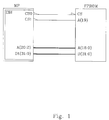
- Figure 1 discloses a memory configuration according to the invention.
- the figure shows a microprocessor MP connected to a dual-plane Flash Programmable Read Only Memory FPROM.
- the FPROM can be programmed or re-programmed after the chip has been soldered onto a chip-board.
- the FPROM comprises a first signal input CS used to activate the memory and a second signal input A19, which is an address input, used to address either one of two planes of the dual-plane memory.
- activation of the address input A(19) represents activation of the nineteenth address bit.
- the FPROM comprises data access lines D(31:0) and address input lines A(18:0). The build up of the FPROM will be further clarified when the next figure in the patent application is explained.
- the microprocessor comprises an external bus interface EBI.
- the bus interface generates signals that control the access to the FPROM.
- the bus interface EBI comprises a first chip-select output CS0 and a second chip-select output CS1.
- the first output CS0 of the microprocessor is connected to the first input CS of the FPROM.
- the second output CS1 of the microprocessor is connected to the second input A19 of the FPROM.
- the external bus interface EBI is configurable and can be programmed to activate the outputs CS0 and CS1 under predetermined conditions.
- the microprocessor in figure 1 comprises nineteen address output lines A(20:2) and thirty-two data access lines Dt(31:0).
- the address output lines A(20:2) of the microprocessor are connected to the address input lines A(18:0) of the FPROM.
- the data access lines Dt(31:0) of the microprocessor are connected to the data access lines D(31:0) of the FPROM.
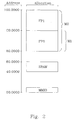
- Figure 2 shows, as an example, a memory map used in the configuration shown above.
- the figure shows hexadecimal notation of addresses and from now on all addresses will be referred to in the patent description by hexadecimal notation.
- the full content of the memory map extends from address 00.0000 to address 100.0000.
- the memory map shown in figure 2 is the memory map that is seen by the microprocessor MP.
- a static random access memory SRAM is located between address 40.0000 and 60.0000 of the memory map.
- the random access memory function as a working memory for the microprocessor MP.
- the memory map I/O MMIO starting from address 00.0000 is used to store input/output interface parameters used by the microprocessor.
- the FPROM that was shown in figure 1 is a so-called dual-plane FPROM that is two independent FPROM chips on the same die.
- This architecture allows one part of the FPROM to be used for program execution while the other part is being erased or reprogrammed.
- the two planes share all control, data and addresses pins, and are usually mapped into separate address spaces of the chip.
- a dual-plane chip of 4Mbit + 4Mbit FPROM looks like an 8Mbit FPROM chip to the external world.
- the two planes are mapped into the lower and upper halves of the address space, respectively.
- the FPROM can also have uneven splits, e.g. 2Mbit + 6Mbit.
- the location of the two planes in the memory map in this example is disclosed in figure 2 .
- a first plane FP0 is located from address 80.0000 to BF.FFFF.
- a second plane FP1 is located from address C0.0000 and FF.FFFF.
- the above shown address distribution of the FPROM implies that the software has to be compiled/linked to a specific FPROM plane. If a particular version of the software has been linked for the FP1 plane, it will not be able to work correct in the FP0 plane, and vice versa. This restriction is in general not acceptable, and therefore the address-spaces need to be swapped, such that the currently used plane, the so-called active plane, always is mapped into one address space (e.g. 80.0000-BF.FFFF). The currently not used plane, the so-called passive FPROM plane, is in the same way mapped into the other address space (e.g. C0.0000-FF.FFFF).
- the invention makes use of the external bus interface EBI located in the microprocessor MP.
- the external bus interface comprises in this example a built-in programmable chip-select generator.
- the chip-select generator has the ability to assert more than one output at the same time. This ability is present on some off-the-shelf micro-controllers, e.g. ATMEL AT91M40800.
- the chip-select generator is configured to always activate the first chip-select output CS0 whenever the FPROM is to be accessed. Assuming now that FP0 is the plane currently used, i.e. the active plane. Beyond CS0, also CS1 is activated (active "low").
- FP1 instead is defined to be the plane currently used, i.e. FP1 is the active plane, the chip-select generator is re-programmed to change the polarity of CS1.
- CS1 now becomes inactive (or active "high") when the FPROM is to be accessed. In this case the address areas C0.0000 to FF.FFFF will be accessed.
- the chip-select signals CS0 and CS1 are used to access the planes.
- CS0 When CS0 is activated the memory area M0 is activated. If also CS1 is activated the area M1 is activated and FP0 is selected. If CS1 instead is inactivated, FP1 is selected.
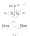
- FIG 3 is disclosed a flow chart showing some of the steps used when the chip-select generator is programmed in accordance with the invention and when it is possible to program the generator to change the polarity of CS1.
- the flow chart is to be read together with the earlier shown figures. The steps are as follows:
- the way to program the chip-select generator of course contains a manifold of different variations depending on which type of chip select generator that is used.
- the chip-select output CS1 referred to above is fixed to be either active "high” or active "low". If the chip-select generator is not able to reprogram the polarity of its outputs, CS1 can be reprogrammed to react on the address range instead. If for example CS1 is fixed active "low” it is possible to change polarity by changing the address area in which CS1 is active. Changing base address for desired plane can do this. A description of this can be found in the description of the microcontroller AT91M40400, Rev.
- the address range which the chip-select outputs respond to can usually be programmed by writing to a single register. In this way the WRITE operation is atomic and this property solves all problems with consistency of the chip-select logic.
- figure 4 is disclosed a flow chart showing some of the steps used when the polarity of CS1 is fixed.
- the first two blocks 101&102 of figure 4a and 4b are the same as the blocks 101&102 already shown in figure 3 .
- the flow chart is to be read together with also the earlier shown figures.
- the steps in figure 4a where CS1 is fixed active "low" are as follows:
- the invention can for example be implemented by ASIC-design, ASIC: Application Specific Integrated Circuits.
- the chip-select generator can be externally located outside the microprocessor.
- the technique to program the configurable chip-select generator varies depending on which type of chip select generator that is used.
- the invention is of course not limited to the above described and in the drawings shown embodiments but can be modified within the scope of the enclosed claims.
Landscapes
- Engineering & Computer Science (AREA)
- Theoretical Computer Science (AREA)
- Physics & Mathematics (AREA)
- General Engineering & Computer Science (AREA)
- General Physics & Mathematics (AREA)
- Microcomputers (AREA)
- Static Random-Access Memory (AREA)
- Signal Processing For Digital Recording And Reproducing (AREA)
- Executing Machine-Instructions (AREA)
- Storage Device Security (AREA)
- Compression, Expansion, Code Conversion, And Decoders (AREA)
- Communication Control (AREA)
- Stored Programmes (AREA)
- Semiconductor Memories (AREA)
Claims (7)
- Anordnung zum Adressieren eines Doppelebenenspeichers (FPROM), wobei der Speicher einen ersten Signaleingang (CS) aufweist, der genutzt wird, um den Speicher zu aktivieren, und einen zweiten Signaleingang (A19), der genutzt wird, um eine von zwei Speicherebenen (FP0; FP1) zu adressieren, wobei die Anordnung einen Mikroprozessor (MP) umfasst, dadurch gekennzeichnet, dass der Mikroprozessor einen Chipauswahlgenerator (EBI) mit einem ersten Chipauswahlausgang (CS0) und einem zweiten Chipauswahlausgang (CS1) umfasst, wobei der erste Chipauswahlausgang (CS0) mit dem ersten Signaleingang (CS) verbunden ist und der zweite Chipauswahlausgang (CS1) mit dem zweiten Signaleingang (A19) verbunden ist, und dadurch, dass die Chipauswahlausgänge (CS0, CS1) und die Signaleingänge (CS, A19) ohne zeitkritische Elemente dazwischen miteinander verbunden sind.
- Anordnung zum Adressieren eines Speichers nach Anspruch 1, wobei der Chipauswahlgenerator (EBI) in den Mikroprozessor (MP) eingebaut ist.
- Anordnung zum Adressieren eines Speichers nach Anspruch 1 oder 2, wobei der Chipauswahlgenerator (EBI) konfigurierbar ist.
- Anordnung zum Adressieren eines Speichers nach einem der Ansprüche 1 - 3, wobei der zweite Chipauswahlausgang (CS1) angeordnet ist, um einen der zwei Speicherebenen (FP0; FP1) in Abhängigkeit davon, welcher der beiden Speicherebenen (FP0; FP1) als aktive Ebene definiert ist, zu adressieren.
- Anordnung zum Adressieren eines Speichers nach einem der Ansprüche 1 - 4, wobei der zweite Chipauswahlausgang (CS1) aktiv "niedrig" ist, wenn eine erste Ebene (FP0) der zwei Speicherebenen als aktive Ebene definiert ist, und wobei der zweite Chipauswahlausgang (CS1) aktiv "hoch" ist, wenn eine zweite Ebene (FP1) der zwei Speicherebenen als aktive Ebene definiert ist.
- Anordnung zum Adressieren eines Speichers nach einem der Ansprüche 1 - 5, wobei der zweite Chipauswahlausgang (CS1) programmiert ist, um auf einen spezifizierten Adressbereich (800000 - BF.FFFF; C0.0000 - FF.FFFF) zu reagieren.
- Anordnung zum Adressieren eines Speichers nach einem der Ansprüche 1 - 6, wobei der erste Chipauswahlausgang (CS0) aktiv "niedrig" ist, wenn auf den Speicher zugegriffen wird.
Applications Claiming Priority (1)
| Application Number | Priority Date | Filing Date | Title |
|---|---|---|---|
| PCT/SE2001/002862 WO2002028162A2 (en) | 2001-12-20 | 2001-12-20 | Penalty free address decoding scheme |
Publications (2)
| Publication Number | Publication Date |
|---|---|
| EP1456757A2 EP1456757A2 (de) | 2004-09-15 |
| EP1456757B1 true EP1456757B1 (de) | 2010-08-04 |
Family
ID=20285155
Family Applications (1)
| Application Number | Title | Priority Date | Filing Date |
|---|---|---|---|
| EP01986244A Expired - Lifetime EP1456757B1 (de) | 2001-12-20 | 2001-12-20 | Adressendecodierungsschema ohne kostenfaktor |
Country Status (7)
| Country | Link |
|---|---|
| US (1) | US20050021901A1 (de) |
| EP (1) | EP1456757B1 (de) |
| CN (1) | CN100380342C (de) |
| AT (1) | ATE476708T1 (de) |
| AU (1) | AU2002217672A1 (de) |
| DE (1) | DE60142752D1 (de) |
| WO (1) | WO2002028162A2 (de) |
Families Citing this family (3)
| Publication number | Priority date | Publication date | Assignee | Title |
|---|---|---|---|---|
| US6961281B2 (en) | 2003-09-12 | 2005-11-01 | Sun Microsystems, Inc. | Single rank memory module for use in a two-rank memory module system |
| US7564735B2 (en) * | 2006-07-05 | 2009-07-21 | Qimonda Ag | Memory device, and method for operating a memory device |
| US9281024B2 (en) | 2014-04-17 | 2016-03-08 | International Business Machines Corporation | Write/read priority blocking scheme using parallel static address decode path |
Family Cites Families (10)
| Publication number | Priority date | Publication date | Assignee | Title |
|---|---|---|---|---|
| US3560943A (en) * | 1968-01-29 | 1971-02-02 | Bell Telephone Labor Inc | Memory organization for two-way access |
| JPH06250931A (ja) * | 1993-02-26 | 1994-09-09 | Mitsubishi Electric Corp | 情報処理装置 |
| US5617559A (en) * | 1994-08-31 | 1997-04-01 | Motorola Inc. | Modular chip select control circuit and method for performing pipelined memory accesses |
| US5913924A (en) * | 1995-12-19 | 1999-06-22 | Adaptec, Inc. | Use of a stored signal to switch between memory banks |
| KR100204027B1 (ko) * | 1996-02-16 | 1999-06-15 | 정선종 | 이중면 비휘발성 메모리를 이용한 데이타베이스 회복 장치 및 그 방법 |
| US5765214A (en) * | 1996-04-22 | 1998-06-09 | Cypress Semiconductor Corporation | Memory access method and apparatus and multi-plane memory device with prefetch |
| US5813041A (en) * | 1996-06-06 | 1998-09-22 | Motorola, Inc. | Method for accessing memory by activating a programmable chip select signal |
| US6260103B1 (en) * | 1998-01-05 | 2001-07-10 | Intel Corporation | Read-while-write memory including fewer verify sense amplifiers than read sense amplifiers |
| JP3920501B2 (ja) * | 1999-04-02 | 2007-05-30 | 株式会社東芝 | 不揮発性半導体記憶装置及びそのデータ消去制御方法 |
| US7046538B2 (en) * | 2004-09-01 | 2006-05-16 | Micron Technology, Inc. | Memory stacking system and method |
-
2001
- 2001-12-20 AT AT01986244T patent/ATE476708T1/de not_active IP Right Cessation
- 2001-12-20 EP EP01986244A patent/EP1456757B1/de not_active Expired - Lifetime
- 2001-12-20 DE DE60142752T patent/DE60142752D1/de not_active Expired - Lifetime
- 2001-12-20 CN CNB01823903XA patent/CN100380342C/zh not_active Expired - Fee Related
- 2001-12-20 WO PCT/SE2001/002862 patent/WO2002028162A2/en not_active Ceased
- 2001-12-20 AU AU2002217672A patent/AU2002217672A1/en not_active Abandoned
- 2001-12-20 US US10/498,750 patent/US20050021901A1/en not_active Abandoned
Also Published As
| Publication number | Publication date |
|---|---|
| AU2002217672A1 (en) | 2002-04-15 |
| CN100380342C (zh) | 2008-04-09 |
| ATE476708T1 (de) | 2010-08-15 |
| DE60142752D1 (de) | 2010-09-16 |
| EP1456757A2 (de) | 2004-09-15 |
| US20050021901A1 (en) | 2005-01-27 |
| CN1672134A (zh) | 2005-09-21 |
| WO2002028162A3 (en) | 2002-10-24 |
| WO2002028162A2 (en) | 2002-04-11 |
Similar Documents
| Publication | Publication Date | Title |
|---|---|---|
| EP0007028B1 (de) | Externe Speichereinrichtung mit Basisregister | |
| US20010052066A1 (en) | Dynamic field patchable microarchitecture | |
| US6047347A (en) | Computer system with programmable bus size | |
| US5987581A (en) | Configurable address line inverter for remapping memory | |
| US7162563B2 (en) | Semiconductor integrated circuit having changeable bus width of external data signal | |
| JPH04229337A (ja) | エミュレータ | |
| US5680632A (en) | Method for providing an extensible register in the first and second data processing systems | |
| EP1456757B1 (de) | Adressendecodierungsschema ohne kostenfaktor | |
| US5748981A (en) | Microcontroller with in-circuit user programmable microcode | |
| HK1004611B (en) | Data processing system providing an extensible register and method thereof | |
| US5961611A (en) | Automatic option setting circuit | |
| US6584540B1 (en) | Flash memory rewriting circuit for microcontroller | |
| JP2003044303A (ja) | コンピュータ装置 | |
| JPH07302254A (ja) | マイクロコンピュータシステム | |
| US6542955B1 (en) | Microcontroller virtual memory system and method | |
| US4138738A (en) | Self-contained relocatable memory subsystem | |
| EP0461631B1 (de) | Datenspeicherungsvorrichtung mit mehreren für eine Adresse bestimmten Registern | |
| EP0864983A2 (de) | Rechnersystem mit Speicheradressensteuerschaltung zum Schutz des Speichers gegen illegales Überschreiben | |
| EP1164490A2 (de) | Rekonfigurierbare Speicherabbildung für ein System auf einem Chip | |
| JPH08305680A (ja) | 半導体装置 | |
| KR100329768B1 (ko) | 마이크로컨트롤러의메모리어드레싱장치 | |
| EP0714060B1 (de) | Ein-Chip-Mikrorechner mit eingebautem nichtflüchtigem Speicher | |
| US20020133687A1 (en) | Facilitating automatic incrementing and/or decrementing of data pointers in a microcontroller | |
| KR940027663A (ko) | 데이타처리시스템의 개발방법 및 데이타처리용 반도체집적회로 | |
| KR20060087038A (ko) | 마이크로컨트롤러 시스템 및 그 롬 데이터 프로그램 방법 |
Legal Events
| Date | Code | Title | Description |
|---|---|---|---|
| PUAI | Public reference made under article 153(3) epc to a published international application that has entered the european phase |
Free format text: ORIGINAL CODE: 0009012 |
|
| 17P | Request for examination filed |
Effective date: 20040607 |
|
| AK | Designated contracting states |
Kind code of ref document: A2 Designated state(s): AT BE CH CY DE DK ES FI FR GB GR IE IT LI LU MC NL PT SE TR |
|
| AX | Request for extension of the european patent |
Extension state: AL LT LV MK RO SI |
|
| 17Q | First examination report despatched |
Effective date: 20090416 |
|
| RIC1 | Information provided on ipc code assigned before grant |
Ipc: G06F 12/06 20060101AFI20090911BHEP |
|
| GRAP | Despatch of communication of intention to grant a patent |
Free format text: ORIGINAL CODE: EPIDOSNIGR1 |
|
| GRAS | Grant fee paid |
Free format text: ORIGINAL CODE: EPIDOSNIGR3 |
|
| GRAA | (expected) grant |
Free format text: ORIGINAL CODE: 0009210 |
|
| AK | Designated contracting states |
Kind code of ref document: B1 Designated state(s): AT BE CH CY DE DK ES FI FR GB GR IE IT LI LU MC NL PT SE TR |
|
| REG | Reference to a national code |
Ref country code: GB Ref legal event code: FG4D |
|
| REG | Reference to a national code |
Ref country code: CH Ref legal event code: EP |
|
| REG | Reference to a national code |
Ref country code: IE Ref legal event code: FG4D |
|
| REF | Corresponds to: |
Ref document number: 60142752 Country of ref document: DE Date of ref document: 20100916 Kind code of ref document: P |
|
| REG | Reference to a national code |
Ref country code: NL Ref legal event code: VDEP Effective date: 20100804 |
|
| PG25 | Lapsed in a contracting state [announced via postgrant information from national office to epo] |
Ref country code: NL Free format text: LAPSE BECAUSE OF FAILURE TO SUBMIT A TRANSLATION OF THE DESCRIPTION OR TO PAY THE FEE WITHIN THE PRESCRIBED TIME-LIMIT Effective date: 20100804 Ref country code: FI Free format text: LAPSE BECAUSE OF FAILURE TO SUBMIT A TRANSLATION OF THE DESCRIPTION OR TO PAY THE FEE WITHIN THE PRESCRIBED TIME-LIMIT Effective date: 20100804 Ref country code: AT Free format text: LAPSE BECAUSE OF FAILURE TO SUBMIT A TRANSLATION OF THE DESCRIPTION OR TO PAY THE FEE WITHIN THE PRESCRIBED TIME-LIMIT Effective date: 20100804 |
|
| PG25 | Lapsed in a contracting state [announced via postgrant information from national office to epo] |
Ref country code: CY Free format text: LAPSE BECAUSE OF FAILURE TO SUBMIT A TRANSLATION OF THE DESCRIPTION OR TO PAY THE FEE WITHIN THE PRESCRIBED TIME-LIMIT Effective date: 20100804 Ref country code: PT Free format text: LAPSE BECAUSE OF FAILURE TO SUBMIT A TRANSLATION OF THE DESCRIPTION OR TO PAY THE FEE WITHIN THE PRESCRIBED TIME-LIMIT Effective date: 20101206 |
|
| PG25 | Lapsed in a contracting state [announced via postgrant information from national office to epo] |
Ref country code: GR Free format text: LAPSE BECAUSE OF FAILURE TO SUBMIT A TRANSLATION OF THE DESCRIPTION OR TO PAY THE FEE WITHIN THE PRESCRIBED TIME-LIMIT Effective date: 20101105 Ref country code: SE Free format text: LAPSE BECAUSE OF FAILURE TO SUBMIT A TRANSLATION OF THE DESCRIPTION OR TO PAY THE FEE WITHIN THE PRESCRIBED TIME-LIMIT Effective date: 20100804 Ref country code: BE Free format text: LAPSE BECAUSE OF FAILURE TO SUBMIT A TRANSLATION OF THE DESCRIPTION OR TO PAY THE FEE WITHIN THE PRESCRIBED TIME-LIMIT Effective date: 20100804 |
|
| PG25 | Lapsed in a contracting state [announced via postgrant information from national office to epo] |
Ref country code: DK Free format text: LAPSE BECAUSE OF FAILURE TO SUBMIT A TRANSLATION OF THE DESCRIPTION OR TO PAY THE FEE WITHIN THE PRESCRIBED TIME-LIMIT Effective date: 20100804 |
|
| PLBE | No opposition filed within time limit |
Free format text: ORIGINAL CODE: 0009261 |
|
| STAA | Information on the status of an ep patent application or granted ep patent |
Free format text: STATUS: NO OPPOSITION FILED WITHIN TIME LIMIT |
|
| PG25 | Lapsed in a contracting state [announced via postgrant information from national office to epo] |
Ref country code: ES Free format text: LAPSE BECAUSE OF FAILURE TO SUBMIT A TRANSLATION OF THE DESCRIPTION OR TO PAY THE FEE WITHIN THE PRESCRIBED TIME-LIMIT Effective date: 20101115 |
|
| 26N | No opposition filed |
Effective date: 20110506 |
|
| PG25 | Lapsed in a contracting state [announced via postgrant information from national office to epo] |
Ref country code: MC Free format text: LAPSE BECAUSE OF NON-PAYMENT OF DUE FEES Effective date: 20101231 |
|
| REG | Reference to a national code |
Ref country code: CH Ref legal event code: PL |
|
| REG | Reference to a national code |
Ref country code: DE Ref legal event code: R097 Ref document number: 60142752 Country of ref document: DE Effective date: 20110506 |
|
| REG | Reference to a national code |
Ref country code: FR Ref legal event code: ST Effective date: 20110831 |
|
| PG25 | Lapsed in a contracting state [announced via postgrant information from national office to epo] |
Ref country code: IE Free format text: LAPSE BECAUSE OF NON-PAYMENT OF DUE FEES Effective date: 20101220 Ref country code: CH Free format text: LAPSE BECAUSE OF NON-PAYMENT OF DUE FEES Effective date: 20101231 Ref country code: LI Free format text: LAPSE BECAUSE OF NON-PAYMENT OF DUE FEES Effective date: 20101231 Ref country code: FR Free format text: LAPSE BECAUSE OF NON-PAYMENT OF DUE FEES Effective date: 20110103 |
|
| PG25 | Lapsed in a contracting state [announced via postgrant information from national office to epo] |
Ref country code: LU Free format text: LAPSE BECAUSE OF NON-PAYMENT OF DUE FEES Effective date: 20101220 |
|
| PG25 | Lapsed in a contracting state [announced via postgrant information from national office to epo] |
Ref country code: TR Free format text: LAPSE BECAUSE OF FAILURE TO SUBMIT A TRANSLATION OF THE DESCRIPTION OR TO PAY THE FEE WITHIN THE PRESCRIBED TIME-LIMIT Effective date: 20100804 |
|
| PGFP | Annual fee paid to national office [announced via postgrant information from national office to epo] |
Ref country code: GB Payment date: 20141229 Year of fee payment: 14 |
|
| PGFP | Annual fee paid to national office [announced via postgrant information from national office to epo] |
Ref country code: DE Payment date: 20141230 Year of fee payment: 14 Ref country code: IT Payment date: 20141224 Year of fee payment: 14 |
|
| REG | Reference to a national code |
Ref country code: DE Ref legal event code: R119 Ref document number: 60142752 Country of ref document: DE |
|
| GBPC | Gb: european patent ceased through non-payment of renewal fee |
Effective date: 20151220 |
|
| PG25 | Lapsed in a contracting state [announced via postgrant information from national office to epo] |
Ref country code: DE Free format text: LAPSE BECAUSE OF NON-PAYMENT OF DUE FEES Effective date: 20160701 Ref country code: GB Free format text: LAPSE BECAUSE OF NON-PAYMENT OF DUE FEES Effective date: 20151220 |
|
| PG25 | Lapsed in a contracting state [announced via postgrant information from national office to epo] |
Ref country code: IT Free format text: LAPSE BECAUSE OF NON-PAYMENT OF DUE FEES Effective date: 20151220 |