EP1453302A2 - Multiplexierung von CMOS Bildaufnahmesensoren auf einen gemeinsamen Datenbus - Google Patents
Multiplexierung von CMOS Bildaufnahmesensoren auf einen gemeinsamen Datenbus Download PDFInfo
- Publication number
- EP1453302A2 EP1453302A2 EP04392005A EP04392005A EP1453302A2 EP 1453302 A2 EP1453302 A2 EP 1453302A2 EP 04392005 A EP04392005 A EP 04392005A EP 04392005 A EP04392005 A EP 04392005A EP 1453302 A2 EP1453302 A2 EP 1453302A2
- Authority
- EP
- European Patent Office
- Prior art keywords
- input
- imager
- line
- imagers
- accessing
- Prior art date
- Legal status (The legal status is an assumption and is not a legal conclusion. Google has not performed a legal analysis and makes no representation as to the accuracy of the status listed.)
- Withdrawn
Links
Images


Classifications
-
- G—PHYSICS
- G06—COMPUTING OR CALCULATING; COUNTING
- G06F—ELECTRIC DIGITAL DATA PROCESSING
- G06F13/00—Interconnection of, or transfer of information or other signals between, memories, input/output devices or central processing units
- G06F13/38—Information transfer, e.g. on bus
-
- H—ELECTRICITY
- H04—ELECTRIC COMMUNICATION TECHNIQUE
- H04N—PICTORIAL COMMUNICATION, e.g. TELEVISION
- H04N25/00—Circuitry of solid-state image sensors [SSIS]; Control thereof
- H04N25/70—SSIS architectures; Circuits associated therewith
- H04N25/76—Addressed sensors, e.g. MOS or CMOS sensors
-
- H—ELECTRICITY
- H04—ELECTRIC COMMUNICATION TECHNIQUE
- H04N—PICTORIAL COMMUNICATION, e.g. TELEVISION
- H04N25/00—Circuitry of solid-state image sensors [SSIS]; Control thereof
- H04N25/40—Extracting pixel data from image sensors by controlling scanning circuits, e.g. by modifying the number of pixels sampled or to be sampled
- H04N25/41—Extracting pixel data from a plurality of image sensors simultaneously picking up an image, e.g. for increasing the field of view by combining the outputs of a plurality of sensors
Definitions
- the invention relates to solid state optical imagers, and, more particularly, to a method to address a reconfigurable array of imagers using a single fixed size data bus.
- Solid state imagers are used in many applications. Typically, these imagers comprise fixed arrays of pixels. It is difficult to reconfigure these imagers into large arrays or into higher resolution arrays. This is especially true when attempting to create high-resolution arrays using fixed data bus architecture.
- U.S. Patent 6,176,429 B1 to Redderson et al describes an optical reader using a photosensor that may comprise a multidimensional CMOS array.
- U.S. Patent 6,505,003 B1 to Malloy Desormeaux discloses a hybrid camera using a CMOS image sensor.
- a principal object of the present invention is to provide an effective and very manufacturable method and device to access an array of imagers.
- a further object of the present invention is to provide a method whereby a plurality of imagers can be used cooperatively to improve image resolution or to provide a single, large resolution image.
- a yet further object of the present invention is to provide a means to reconfigure an n x m array of imagers using a single data bus architecture.
- a method of addressing imagers comprises, first, providing a bi-directional bus.
- An array of imagers is arranged in n rows and m columns wherein the n and m are positive integers.
- Each imager is connected to the bi-directional bus.
- Each imager has a Vmode terminal.
- Each imager has a select terminal.
- Each imager can deliver a signal to the bi-directional bus only when a first selecting signal is applied to a Vmode terminal of that imager and a second selecting signal is applied to a select terminal of that imager simultaneously.
- a first multiplexer has a vertical select input and n outputs. Each of the n outputs is connected to one of the Vmode terminals of the imagers.
- a second multiplexer has a horizontal select input and n x m outputs. Each output is connected to the select terminal of one of the imagers.
- a vertical input signal is applied to the vertical select input of the first multiplexer thereby producing the first selecting signal at one of the Vmode output lines.
- a horizontal input signal is applied to the horizontal select input of the second multiplexer thereby sequentially producing the second selecting signal at the select terminal of one of the imagers.
- a method of accessing an imager array comprises, first, providing a bi-directional bus.
- An array of imagers is arranged in n rows and m columns. The n and m are positive integers. Each imager is connected to the bi-directional bus.
- a line of bits of any imager is accessible by a line address.
- a column counter, a row counter, and the line address are initialized to zero. All of the array is accessed.
- the accessing comprises further steps of, first, accessing one line of one the imager corresponding to the line address, the column counter, and the row counter. Thereafter the column counter is tested for equality to m-1.
- the column counter is incremented and the step of accessing one line is repeated. If equal, the column counter is reset. Thereafter the line address is tested for equality to total lines in each imager. If not equal, the line address is incremented and the step of accessing one line is repeated. If equal, the line address is reset. Thereafter the row counter is tested for equality to n-1. If not equal, the row counter is incremented and the step of accessing one line is repeated. If equal, the step of accessing all is completed.
- a multiple imager array device comprises, first, a bi-directional bus.
- An array of imagers is arranged in n rows and m columns. The n and m are positive integers.
- Each imager is connected to the bi-directional bus.
- a line of bits of any imager is accessible by a line address.
- Each imager has a Vmode input and an output enable input. The Vmode input and the output enable input must be enabled to allow accessing.
- a first multiplexer has an input and a plurality of outputs. The input is connected to a column counter. Each output is connected to the output enable input of one of the imagers.
- a second multiplexer has an input and a plurality of outputs. The input is connected to a row counter. Each output is connected to the Vmode input of each imager in one of the rows.
- the preferred embodiments of the present invention disclose a method and a device for accessing an imager array having a single, bi-directional bus. It should be clear to those experienced in the art that the present invention can be applied and extended without deviating from the scope of the present invention.
- Fig. 1 the first preferred embodiment of the present invention is illustrated. Several important features of the present invention are shown and discussed below.
- This invention relates to an n x m array of imagers connected to a single bi-directional bus.
- a 2 x 3 array of six imagers 101, 102, 103, 210, 202, and 203 with each of the imagers connected to a single bi-directional bus 100 is shown in Fig. 1.
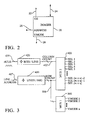
- An example of a single imager 20 is shown in Fig. 2.
- This imager has an output port 24 for connection to the bus.
- a signal at the Vmode terminal 22 controls whether or not the imager 20 is connected to the bus.
- a select terminal 26 selects a particular imager 20.
- An address bus ADDRESS 28 is used to select which row or line of bits is accessed. For the imager to deliver a signal to the bus both the Vmode terminal 20 and the select terminal 26 must be activated.
- the six imagers are arranged in an array of two rows of three imagers in each row.
- Imagers 101, 102, and 103 are in the first row and have output ports 110, 112, and 114 connected to the bi-directional bus 100.
- Imagers 201, 202, and 203 are in the second row and have output ports 210, 212, and 214 connected to the bi-directional bus 100.
- a vertical select line 306 is connected to a first multiplexer 300.
- the first multiplexer 300 has a Vmode output line for each row of imagers.
- the first multiplexer 300 has a first Vmode line 302 and a second Vmode line 304.
- the first Vmode line 302 is connected to the Vmode terminals 104, 106, and 108 of the imagers 101, 102, and 103 in the first row.
- the second Vmode line 304 is connected to the Vmode terminals 204, 206, and 208 of the imagers 201, 202, and 203 in the first row. If there were more imagers in each row of the array, the Vmode terminals of all the imagers in the first row would be connected to the first Vmode line, and the Vmode terminals of all the imagers in the second row would be connected to the second Vmode line. If there were additional rows of imagers, then the first multiplexer 300 would have a Vmode line for each row of imagers in the array.
- the input to the first multiplexer 300 is a vertical select line 306.
- a horizontal select line, COLUMN COUNT, 402 is connected to a second multiplexer 400 which has an output line for each imager in the array.
- One of the output lines of the second multiplexer 400 is connected to the select terminal 116, 118, 120, 216, 218, and 220 of each imager 101, 102, 103, 201, 202, and 202 in the array.
- the vertical select line, ROW COUNT, 306 causes the multiplexer to activate either the first Vmode line 302 or the second Vmode line 304.
- the horizontal select line then causes the second multiplexer 400 to activate the select terminal of a particular imager so that the signal from that imager is sent to the bi-directional bus 100.
- the vertical address selects the n imagers in row m.
- the input to the second multiplexer 400 then causes an output of the second multiplexer 400 to enable the output port of a single imager to be active and the signal of that imager to be transferred to the bi-directional bus 100.
- the vertical select address as the write enable pulse, an entire row is selected and transferred to n horizontal registers. This line is read out serially.
- This method provides a means to reconfigure the array of imagers n x m without bounds while maintaining the same data bus architecture.
- This application could be implemented with slightly overlapping optics to provide a seamless combining of imager data to provide a single, large resolution image.
- This has application in fixed object plane imaging which includes X-ray imagers and facsimile. Also, several remote sources could be multiplexed onto a single display for security applications.
- the device comprises, first, a bi-directional bus 100.
- Each imager is connected 110, 112, 114, 210, 212, and 214 to the bi-directional bus 100.
- a line of bits of any imager is accessible by a line address LINE ADDRESS 407.
- Each imager 101, 102, 103, 201, 202, and 203 has a Vmode input and an output enable input. The Vmode input and the output enable input must be enabled to allow accessing.
- a first multiplexer MUX2 400 has an input 402 and a plurality of outputs SEL1-SEL6 116, 118, 120, 216, 218, and 220. The input is connected to a column counter COLUMN COUNT 402. Each output SEL1-SEL6 is connected to the output enable input of one of the imagers I1-I6.
- a second multiplexer MUX1 300 has an input 306 and a plurality of outputs 302 and 304. The input is connected to a row counter ROW COUNT 306. Each output VMODE1 302 and VMODE2 304 is connected to the Vmode input of each imager in one of the rows.
- the horizontal clock HCLK 435 comprises a synchronous clock used to clock data into or out from the imager devices in the array.
- the HCLK 435 comprises a 36 MHz signal.
- a first divider 420 is used to divide the HCLK 435 by the number of horizontal bits per line in each imager. For example, if the imagers are each 640 bits/line x 480 lines, then the HCLK 435 is divided by 640 to create the signal COLUMN COUNT 402.
- the COLUMN COUNT 402 is a multiple bit signal that effectively counts each time an imager is read by the HCLK signal.
- the LINE ADDRESS signal 407 comprises the address bus used to select which row of any imager is read/written.
- the LINE ADDRESS signal 407 is divided by the number of lines (rows) in each imager. In the preferred case, this means that the LINE ADDRESS signal is divided by 480 to create the ROW COUNT 306. Therefore, the LINE ADDRESS between 0 and 479 reads the top row of imagers, the LINE ADDRESS between 480 and 959 reads the bottom row of imagers. Since there are only two rows of imagers in the preferred embodiment, the ROW COUNT 306 is only 0 or 1 and can be carried by a single line.
- the COLUMN COUNT 402 and the ROW COUNT 306 are both input into the first multiplexer MUX2 400.
- the combined sum can be written COLUMN COUNT:ROW COUNT as a bus input to the MUX2 400.
- the outputs of the first multiplexer MUX2 400 are the selection signals SEL1 to SEL(mxn) in the general case.
- the ROW COUNT signal is used by the second multiplexer MUX1 300 to generate the Vmode signals VMODE1 to VMODEn in the general case.
- the method 500 of accessing (read/write) imager data in an imager array comprises initializing the column counter, the row counter, and the line address to zero in step 510.
- One line of one the imager is accessed corresponding to the line address, the column counter, and the row counter in step 515.
- the column counter is tested for equality to m-1 in step 520. If not equal, the column counter is incremented and the step of accessing one line is repeated in step 525. If equal, the column counter is reset in step 530. Thereafter the line address is tested for equality to total lines in each imager in step 535.
- step 540 If not equal, the line address is incremented and the step of accessing one line is repeated in step 540. If equal, the line address is reset in step 545. Thereafter the row counter is tested for equality to n-1 in step 550. If not equal, the row counter is incremented and the step of accessing one line is repeated in step 555. If equal, the step of accessing all is completed.
- An effective and very manufacturable method and device to access an array of imagers is achieved.
- a method whereby a plurality of imagers can be used cooperatively to improve image resolution or to provide a single, large resolution image is achieved.
- a means to reconfigure an n x m array of imagers using a single data bus architecture is provided.
- the novel method and device of the present invention provides an effective and manufacturable alternative to the prior art.
Landscapes
- Engineering & Computer Science (AREA)
- Multimedia (AREA)
- Signal Processing (AREA)
- Theoretical Computer Science (AREA)
- Physics & Mathematics (AREA)
- General Engineering & Computer Science (AREA)
- General Physics & Mathematics (AREA)
- Transforming Light Signals Into Electric Signals (AREA)
Applications Claiming Priority (2)
| Application Number | Priority Date | Filing Date | Title |
|---|---|---|---|
| US45008603P | 2003-02-26 | 2003-02-26 | |
| US450086 | 2003-02-26 |
Publications (1)
| Publication Number | Publication Date |
|---|---|
| EP1453302A2 true EP1453302A2 (de) | 2004-09-01 |
Family
ID=32825424
Family Applications (1)
| Application Number | Title | Priority Date | Filing Date |
|---|---|---|---|
| EP04392005A Withdrawn EP1453302A2 (de) | 2003-02-26 | 2004-02-24 | Multiplexierung von CMOS Bildaufnahmesensoren auf einen gemeinsamen Datenbus |
Country Status (4)
| Country | Link |
|---|---|
| US (1) | US7324145B2 (de) |
| EP (1) | EP1453302A2 (de) |
| JP (1) | JP2004260827A (de) |
| KR (1) | KR20040076827A (de) |
Families Citing this family (1)
| Publication number | Priority date | Publication date | Assignee | Title |
|---|---|---|---|---|
| KR101377269B1 (ko) * | 2008-01-28 | 2014-03-24 | 삼성전자주식회사 | 고속으로 대용량의 직렬 데이터를 전송할 수 있는 이미지센서 |
Family Cites Families (7)
| Publication number | Priority date | Publication date | Assignee | Title |
|---|---|---|---|---|
| US5134488A (en) * | 1990-12-28 | 1992-07-28 | David Sarnoff Research Center, Inc. | X-Y addressable imager with variable integration |
| US5719626A (en) * | 1994-12-16 | 1998-02-17 | Nikon Corporation | Solid-state image pickup device |
| WO1997007630A1 (en) * | 1995-08-11 | 1997-02-27 | Kabushiki Kaisha Toshiba | Mos image pickup device |
| US5973311A (en) * | 1997-02-12 | 1999-10-26 | Imation Corp | Pixel array with high and low resolution mode |
| US6176429B1 (en) | 1998-07-17 | 2001-01-23 | Psc Scanning, Inc. | Optical reader with selectable processing characteristics for reading data in multiple formats |
| US6507365B1 (en) * | 1998-11-30 | 2003-01-14 | Kabushiki Kaisha Toshiba | Solid-state imaging device |
| US6505003B1 (en) | 2001-10-12 | 2003-01-07 | Eastman Kodak Company | Hybrid cameras that revise stored electronic image metadata at film unit removal and methods |
-
2004
- 2004-01-27 US US10/766,648 patent/US7324145B2/en not_active Expired - Lifetime
- 2004-02-24 EP EP04392005A patent/EP1453302A2/de not_active Withdrawn
- 2004-02-25 JP JP2004049326A patent/JP2004260827A/ja active Pending
- 2004-02-26 KR KR1020040013071A patent/KR20040076827A/ko not_active Withdrawn
Also Published As
| Publication number | Publication date |
|---|---|
| JP2004260827A (ja) | 2004-09-16 |
| US7324145B2 (en) | 2008-01-29 |
| US20040189840A1 (en) | 2004-09-30 |
| KR20040076827A (ko) | 2004-09-03 |
Similar Documents
| Publication | Publication Date | Title |
|---|---|---|
| US6480921B1 (en) | Reducing internal bus speed in a bus system without reducing readout rate | |
| US20020018600A1 (en) | Image scanning circuitry with row and column addressing for use in electronic cameras | |
| EP4160680A1 (de) | Bildsensor mit grossem dynamikbereich | |
| US4602275A (en) | Television memory system | |
| US5523788A (en) | Image processor with input buffering to multiple digital signal processors | |
| JP2004023279A (ja) | 半導体装置、携帯端末システムおよびセンサモジュール | |
| US5854656A (en) | Non-uniform clocking system for area imaging device | |
| EP1453303A2 (de) | Simultanes Auslesen von Zeilen in CMOS APS Bildaufnehmern | |
| US20050104982A1 (en) | Pixel arranging apparatus, solid-state image sensing apparatus,and camera | |
| EP0260997B1 (de) | Verarbeitung von Videobildsignalen | |
| US7551189B2 (en) | Method of and apparatus for digital image processing | |
| US6542429B2 (en) | Method of controlling line memory | |
| US7324145B2 (en) | Multiplexing prism CMOS imagers to a single data bus | |
| US7619195B2 (en) | Imaging device driver, imaging device driving method, and image signal processor | |
| JP3707820B2 (ja) | 高速撮影装置 | |
| JP2690312B2 (ja) | 映像信号のディジタル記憶装置 | |
| US6727947B1 (en) | Digital camera | |
| JP3573406B2 (ja) | 画像処理装置 | |
| JPH01109890A (ja) | デマルチプレクサ | |
| JP3655159B2 (ja) | 表示装置 | |
| CN114638741A (zh) | 图像显示方法、装置和系统 | |
| US20040145666A1 (en) | Solid state imaging apparatus, method for driving the same and camera using the same | |
| CN100384243C (zh) | 一种用于空间试验的静态图像采集系统 | |
| JP3458203B2 (ja) | 画像処理装置 | |
| KR100224754B1 (ko) | 비디오 프레임 메모리 장치 및 비디오 데이터 처리방법 |
Legal Events
| Date | Code | Title | Description |
|---|---|---|---|
| PUAI | Public reference made under article 153(3) epc to a published international application that has entered the european phase |
Free format text: ORIGINAL CODE: 0009012 |
|
| AK | Designated contracting states |
Kind code of ref document: A2 Designated state(s): AT BE BG CH CY CZ DE DK EE ES FI FR GB GR HU IE IT LI LU MC NL PT RO SE SI SK TR |
|
| AX | Request for extension of the european patent |
Extension state: AL HR LT LV MK |
|
| STAA | Information on the status of an ep patent application or granted ep patent |
Free format text: STATUS: THE APPLICATION IS DEEMED TO BE WITHDRAWN |
|
| 18D | Application deemed to be withdrawn |
Effective date: 20060901 |