EP1447786A1 - Active matrix substrate, electro-optical apparatus, and electronic device - Google Patents
Active matrix substrate, electro-optical apparatus, and electronic device Download PDFInfo
- Publication number
- EP1447786A1 EP1447786A1 EP02803559A EP02803559A EP1447786A1 EP 1447786 A1 EP1447786 A1 EP 1447786A1 EP 02803559 A EP02803559 A EP 02803559A EP 02803559 A EP02803559 A EP 02803559A EP 1447786 A1 EP1447786 A1 EP 1447786A1
- Authority
- EP
- European Patent Office
- Prior art keywords
- electro
- layer
- terminal
- light
- electrode
- Prior art date
- Legal status (The legal status is an assumption and is not a legal conclusion. Google has not performed a legal analysis and makes no representation as to the accuracy of the status listed.)
- Withdrawn
Links
Images





Classifications
-
- G—PHYSICS
- G09—EDUCATION; CRYPTOGRAPHY; DISPLAY; ADVERTISING; SEALS
- G09G—ARRANGEMENTS OR CIRCUITS FOR CONTROL OF INDICATING DEVICES USING STATIC MEANS TO PRESENT VARIABLE INFORMATION
- G09G3/00—Control arrangements or circuits, of interest only in connection with visual indicators other than cathode-ray tubes
- G09G3/20—Control arrangements or circuits, of interest only in connection with visual indicators other than cathode-ray tubes for presentation of an assembly of a number of characters, e.g. a page, by composing the assembly by combination of individual elements arranged in a matrix no fixed position being assigned to or needed to be assigned to the individual characters or partial characters
- G09G3/22—Control arrangements or circuits, of interest only in connection with visual indicators other than cathode-ray tubes for presentation of an assembly of a number of characters, e.g. a page, by composing the assembly by combination of individual elements arranged in a matrix no fixed position being assigned to or needed to be assigned to the individual characters or partial characters using controlled light sources
- G09G3/30—Control arrangements or circuits, of interest only in connection with visual indicators other than cathode-ray tubes for presentation of an assembly of a number of characters, e.g. a page, by composing the assembly by combination of individual elements arranged in a matrix no fixed position being assigned to or needed to be assigned to the individual characters or partial characters using controlled light sources using electroluminescent panels
- G09G3/32—Control arrangements or circuits, of interest only in connection with visual indicators other than cathode-ray tubes for presentation of an assembly of a number of characters, e.g. a page, by composing the assembly by combination of individual elements arranged in a matrix no fixed position being assigned to or needed to be assigned to the individual characters or partial characters using controlled light sources using electroluminescent panels semiconductive, e.g. using light-emitting diodes [LED]
- G09G3/3208—Control arrangements or circuits, of interest only in connection with visual indicators other than cathode-ray tubes for presentation of an assembly of a number of characters, e.g. a page, by composing the assembly by combination of individual elements arranged in a matrix no fixed position being assigned to or needed to be assigned to the individual characters or partial characters using controlled light sources using electroluminescent panels semiconductive, e.g. using light-emitting diodes [LED] organic, e.g. using organic light-emitting diodes [OLED]
- G09G3/3225—Control arrangements or circuits, of interest only in connection with visual indicators other than cathode-ray tubes for presentation of an assembly of a number of characters, e.g. a page, by composing the assembly by combination of individual elements arranged in a matrix no fixed position being assigned to or needed to be assigned to the individual characters or partial characters using controlled light sources using electroluminescent panels semiconductive, e.g. using light-emitting diodes [LED] organic, e.g. using organic light-emitting diodes [OLED] using an active matrix
- G09G3/3233—Control arrangements or circuits, of interest only in connection with visual indicators other than cathode-ray tubes for presentation of an assembly of a number of characters, e.g. a page, by composing the assembly by combination of individual elements arranged in a matrix no fixed position being assigned to or needed to be assigned to the individual characters or partial characters using controlled light sources using electroluminescent panels semiconductive, e.g. using light-emitting diodes [LED] organic, e.g. using organic light-emitting diodes [OLED] using an active matrix with pixel circuitry controlling the current through the light-emitting element
- G09G3/3241—Control arrangements or circuits, of interest only in connection with visual indicators other than cathode-ray tubes for presentation of an assembly of a number of characters, e.g. a page, by composing the assembly by combination of individual elements arranged in a matrix no fixed position being assigned to or needed to be assigned to the individual characters or partial characters using controlled light sources using electroluminescent panels semiconductive, e.g. using light-emitting diodes [LED] organic, e.g. using organic light-emitting diodes [OLED] using an active matrix with pixel circuitry controlling the current through the light-emitting element the current through the light-emitting element being set using a data current provided by the data driver, e.g. by using a two-transistor current mirror
- G09G3/325—Control arrangements or circuits, of interest only in connection with visual indicators other than cathode-ray tubes for presentation of an assembly of a number of characters, e.g. a page, by composing the assembly by combination of individual elements arranged in a matrix no fixed position being assigned to or needed to be assigned to the individual characters or partial characters using controlled light sources using electroluminescent panels semiconductive, e.g. using light-emitting diodes [LED] organic, e.g. using organic light-emitting diodes [OLED] using an active matrix with pixel circuitry controlling the current through the light-emitting element the current through the light-emitting element being set using a data current provided by the data driver, e.g. by using a two-transistor current mirror the data current flowing through the driving transistor during a setting phase, e.g. by using a switch for connecting the driving transistor to the data driver
-
- H—ELECTRICITY
- H10—SEMICONDUCTOR DEVICES; ELECTRIC SOLID-STATE DEVICES NOT OTHERWISE PROVIDED FOR
- H10H—INORGANIC LIGHT-EMITTING SEMICONDUCTOR DEVICES HAVING POTENTIAL BARRIERS
- H10H20/00—Individual inorganic light-emitting semiconductor devices having potential barriers, e.g. light-emitting diodes [LED]
- H10H20/80—Constructional details
- H10H20/81—Bodies
- H10H20/813—Bodies having a plurality of light-emitting regions, e.g. multi-junction LEDs or light-emitting devices having photoluminescent regions within the bodies
-
- H—ELECTRICITY
- H10—SEMICONDUCTOR DEVICES; ELECTRIC SOLID-STATE DEVICES NOT OTHERWISE PROVIDED FOR
- H10D—INORGANIC ELECTRIC SEMICONDUCTOR DEVICES
- H10D30/00—Field-effect transistors [FET]
- H10D30/60—Insulated-gate field-effect transistors [IGFET]
- H10D30/67—Thin-film transistors [TFT]
- H10D30/6704—Thin-film transistors [TFT] having supplementary regions or layers in the thin films or in the insulated bulk substrates for controlling properties of the device
- H10D30/6706—Thin-film transistors [TFT] having supplementary regions or layers in the thin films or in the insulated bulk substrates for controlling properties of the device for preventing leakage current
-
- H—ELECTRICITY
- H10—SEMICONDUCTOR DEVICES; ELECTRIC SOLID-STATE DEVICES NOT OTHERWISE PROVIDED FOR
- H10D—INORGANIC ELECTRIC SEMICONDUCTOR DEVICES
- H10D30/00—Field-effect transistors [FET]
- H10D30/60—Insulated-gate field-effect transistors [IGFET]
- H10D30/67—Thin-film transistors [TFT]
- H10D30/6704—Thin-film transistors [TFT] having supplementary regions or layers in the thin films or in the insulated bulk substrates for controlling properties of the device
- H10D30/6713—Thin-film transistors [TFT] having supplementary regions or layers in the thin films or in the insulated bulk substrates for controlling properties of the device characterised by the properties of the source or drain regions, e.g. compositions or sectional shapes
- H10D30/6715—Thin-film transistors [TFT] having supplementary regions or layers in the thin films or in the insulated bulk substrates for controlling properties of the device characterised by the properties of the source or drain regions, e.g. compositions or sectional shapes characterised by the doping profiles, e.g. having lightly-doped source or drain extensions
-
- H—ELECTRICITY
- H10—SEMICONDUCTOR DEVICES; ELECTRIC SOLID-STATE DEVICES NOT OTHERWISE PROVIDED FOR
- H10D—INORGANIC ELECTRIC SEMICONDUCTOR DEVICES
- H10D30/00—Field-effect transistors [FET]
- H10D30/60—Insulated-gate field-effect transistors [IGFET]
- H10D30/67—Thin-film transistors [TFT]
- H10D30/6729—Thin-film transistors [TFT] characterised by the electrodes
- H10D30/673—Thin-film transistors [TFT] characterised by the electrodes characterised by the shapes, relative sizes or dispositions of the gate electrodes
- H10D30/6733—Multi-gate TFTs
-
- H—ELECTRICITY
- H10—SEMICONDUCTOR DEVICES; ELECTRIC SOLID-STATE DEVICES NOT OTHERWISE PROVIDED FOR
- H10D—INORGANIC ELECTRIC SEMICONDUCTOR DEVICES
- H10D30/00—Field-effect transistors [FET]
- H10D30/60—Insulated-gate field-effect transistors [IGFET]
- H10D30/67—Thin-film transistors [TFT]
- H10D30/674—Thin-film transistors [TFT] characterised by the active materials
-
- H—ELECTRICITY
- H10—SEMICONDUCTOR DEVICES; ELECTRIC SOLID-STATE DEVICES NOT OTHERWISE PROVIDED FOR
- H10D—INORGANIC ELECTRIC SEMICONDUCTOR DEVICES
- H10D86/00—Integrated devices formed in or on insulating or conducting substrates, e.g. formed in silicon-on-insulator [SOI] substrates or on stainless steel or glass substrates
- H10D86/40—Integrated devices formed in or on insulating or conducting substrates, e.g. formed in silicon-on-insulator [SOI] substrates or on stainless steel or glass substrates characterised by multiple TFTs
- H10D86/441—Interconnections, e.g. scanning lines
-
- H—ELECTRICITY
- H10—SEMICONDUCTOR DEVICES; ELECTRIC SOLID-STATE DEVICES NOT OTHERWISE PROVIDED FOR
- H10D—INORGANIC ELECTRIC SEMICONDUCTOR DEVICES
- H10D86/00—Integrated devices formed in or on insulating or conducting substrates, e.g. formed in silicon-on-insulator [SOI] substrates or on stainless steel or glass substrates
- H10D86/40—Integrated devices formed in or on insulating or conducting substrates, e.g. formed in silicon-on-insulator [SOI] substrates or on stainless steel or glass substrates characterised by multiple TFTs
- H10D86/60—Integrated devices formed in or on insulating or conducting substrates, e.g. formed in silicon-on-insulator [SOI] substrates or on stainless steel or glass substrates characterised by multiple TFTs wherein the TFTs are in active matrices
-
- H—ELECTRICITY
- H10—SEMICONDUCTOR DEVICES; ELECTRIC SOLID-STATE DEVICES NOT OTHERWISE PROVIDED FOR
- H10K—ORGANIC ELECTRIC SOLID-STATE DEVICES
- H10K59/00—Integrated devices, or assemblies of multiple devices, comprising at least one organic light-emitting element covered by group H10K50/00
- H10K59/10—OLED displays
- H10K59/12—Active-matrix OLED [AMOLED] displays
- H10K59/121—Active-matrix OLED [AMOLED] displays characterised by the geometry or disposition of pixel elements
-
- H—ELECTRICITY
- H10—SEMICONDUCTOR DEVICES; ELECTRIC SOLID-STATE DEVICES NOT OTHERWISE PROVIDED FOR
- H10K—ORGANIC ELECTRIC SOLID-STATE DEVICES
- H10K59/00—Integrated devices, or assemblies of multiple devices, comprising at least one organic light-emitting element covered by group H10K50/00
- H10K59/10—OLED displays
- H10K59/12—Active-matrix OLED [AMOLED] displays
- H10K59/121—Active-matrix OLED [AMOLED] displays characterised by the geometry or disposition of pixel elements
- H10K59/1213—Active-matrix OLED [AMOLED] displays characterised by the geometry or disposition of pixel elements the pixel elements being TFTs
-
- H—ELECTRICITY
- H10—SEMICONDUCTOR DEVICES; ELECTRIC SOLID-STATE DEVICES NOT OTHERWISE PROVIDED FOR
- H10K—ORGANIC ELECTRIC SOLID-STATE DEVICES
- H10K59/00—Integrated devices, or assemblies of multiple devices, comprising at least one organic light-emitting element covered by group H10K50/00
- H10K59/10—OLED displays
- H10K59/12—Active-matrix OLED [AMOLED] displays
- H10K59/121—Active-matrix OLED [AMOLED] displays characterised by the geometry or disposition of pixel elements
- H10K59/1216—Active-matrix OLED [AMOLED] displays characterised by the geometry or disposition of pixel elements the pixel elements being capacitors
-
- H—ELECTRICITY
- H10—SEMICONDUCTOR DEVICES; ELECTRIC SOLID-STATE DEVICES NOT OTHERWISE PROVIDED FOR
- H10K—ORGANIC ELECTRIC SOLID-STATE DEVICES
- H10K59/00—Integrated devices, or assemblies of multiple devices, comprising at least one organic light-emitting element covered by group H10K50/00
- H10K59/10—OLED displays
- H10K59/12—Active-matrix OLED [AMOLED] displays
- H10K59/131—Interconnections, e.g. wiring lines or terminals
-
- G—PHYSICS
- G02—OPTICS
- G02F—OPTICAL DEVICES OR ARRANGEMENTS FOR THE CONTROL OF LIGHT BY MODIFICATION OF THE OPTICAL PROPERTIES OF THE MEDIA OF THE ELEMENTS INVOLVED THEREIN; NON-LINEAR OPTICS; FREQUENCY-CHANGING OF LIGHT; OPTICAL LOGIC ELEMENTS; OPTICAL ANALOGUE/DIGITAL CONVERTERS
- G02F1/00—Devices or arrangements for the control of the intensity, colour, phase, polarisation or direction of light arriving from an independent light source, e.g. switching, gating or modulating; Non-linear optics
- G02F1/01—Devices or arrangements for the control of the intensity, colour, phase, polarisation or direction of light arriving from an independent light source, e.g. switching, gating or modulating; Non-linear optics for the control of the intensity, phase, polarisation or colour
- G02F1/13—Devices or arrangements for the control of the intensity, colour, phase, polarisation or direction of light arriving from an independent light source, e.g. switching, gating or modulating; Non-linear optics for the control of the intensity, phase, polarisation or colour based on liquid crystals, e.g. single liquid crystal display cells
- G02F1/133—Constructional arrangements; Operation of liquid crystal cells; Circuit arrangements
- G02F1/136—Liquid crystal cells structurally associated with a semi-conducting layer or substrate, e.g. cells forming part of an integrated circuit
- G02F1/1362—Active matrix addressed cells
- G02F1/1368—Active matrix addressed cells in which the switching element is a three-electrode device
-
- G—PHYSICS
- G09—EDUCATION; CRYPTOGRAPHY; DISPLAY; ADVERTISING; SEALS
- G09G—ARRANGEMENTS OR CIRCUITS FOR CONTROL OF INDICATING DEVICES USING STATIC MEANS TO PRESENT VARIABLE INFORMATION
- G09G2300/00—Aspects of the constitution of display devices
- G09G2300/04—Structural and physical details of display devices
- G09G2300/0404—Matrix technologies
- G09G2300/0417—Special arrangements specific to the use of low carrier mobility technology
-
- G—PHYSICS
- G09—EDUCATION; CRYPTOGRAPHY; DISPLAY; ADVERTISING; SEALS
- G09G—ARRANGEMENTS OR CIRCUITS FOR CONTROL OF INDICATING DEVICES USING STATIC MEANS TO PRESENT VARIABLE INFORMATION
- G09G2300/00—Aspects of the constitution of display devices
- G09G2300/08—Active matrix structure, i.e. with use of active elements, inclusive of non-linear two terminal elements, in the pixels together with light emitting or modulating elements
- G09G2300/0809—Several active elements per pixel in active matrix panels
- G09G2300/0842—Several active elements per pixel in active matrix panels forming a memory circuit, e.g. a dynamic memory with one capacitor
-
- G—PHYSICS
- G09—EDUCATION; CRYPTOGRAPHY; DISPLAY; ADVERTISING; SEALS
- G09G—ARRANGEMENTS OR CIRCUITS FOR CONTROL OF INDICATING DEVICES USING STATIC MEANS TO PRESENT VARIABLE INFORMATION
- G09G2300/00—Aspects of the constitution of display devices
- G09G2300/08—Active matrix structure, i.e. with use of active elements, inclusive of non-linear two terminal elements, in the pixels together with light emitting or modulating elements
- G09G2300/0809—Several active elements per pixel in active matrix panels
- G09G2300/0842—Several active elements per pixel in active matrix panels forming a memory circuit, e.g. a dynamic memory with one capacitor
- G09G2300/0861—Several active elements per pixel in active matrix panels forming a memory circuit, e.g. a dynamic memory with one capacitor with additional control of the display period without amending the charge stored in a pixel memory, e.g. by means of additional select electrodes
-
- G—PHYSICS
- G09—EDUCATION; CRYPTOGRAPHY; DISPLAY; ADVERTISING; SEALS
- G09G—ARRANGEMENTS OR CIRCUITS FOR CONTROL OF INDICATING DEVICES USING STATIC MEANS TO PRESENT VARIABLE INFORMATION
- G09G2320/00—Control of display operating conditions
- G09G2320/02—Improving the quality of display appearance
-
- G—PHYSICS
- G09—EDUCATION; CRYPTOGRAPHY; DISPLAY; ADVERTISING; SEALS
- G09G—ARRANGEMENTS OR CIRCUITS FOR CONTROL OF INDICATING DEVICES USING STATIC MEANS TO PRESENT VARIABLE INFORMATION
- G09G2320/00—Control of display operating conditions
- G09G2320/02—Improving the quality of display appearance
- G09G2320/0209—Crosstalk reduction, i.e. to reduce direct or indirect influences of signals directed to a certain pixel of the displayed image on other pixels of said image, inclusive of influences affecting pixels in different frames or fields or sub-images which constitute a same image, e.g. left and right images of a stereoscopic display
- G09G2320/0214—Crosstalk reduction, i.e. to reduce direct or indirect influences of signals directed to a certain pixel of the displayed image on other pixels of said image, inclusive of influences affecting pixels in different frames or fields or sub-images which constitute a same image, e.g. left and right images of a stereoscopic display with crosstalk due to leakage current of pixel switch in active matrix panels
Definitions
- This invention relates to an active matrix substrate suitable for electro-optical devices, an electro-optical device, and electronic device.
- the active matrix driving method is one method of driving electro-optical devices comprising liquid crystal elements, organic electroluminescence (EL) elements, electrophoretic elements, electronic emission elements, and similar.
- a plurality of pixels are arranged in a matrix on the display panel.
- Each of the plurality of pixels comprises a pixel circuit, in turn comprising an electro-optical element and a driving transistor which supplies driving power to the electro-optical element.
- Each of the plurality of pixel circuits is arranged to correspond to the intersection of a data line and a scan line (see, for example, patent reference 1: Internationally disclosed pamphlet no. WO98/36407).
- the amount of power supplied to electro-optical elements must be precisely controlled.
- organic EL elements are current-driving type electro-optical elements, the brightness is directly affected by the current.
- the pixel layout must also be optimized. Problems encountered in actual pixel layouts include, for example, contact between pixel electrodes and peripheral circuitry, stability of holding capacitances, and transistor turn-off currents.
- the present invention was devised in light of the above circumstances, and has as an object the provision of an active matrix substrate, electro-optical device, and electronic device comprising an optimal pixel layout for the stable driving of electro-optical elements.
- a first active matrix substrate of this invention is an active matrix substrate comprising peripheral circuitry to supply a current to electro-optical elements provided in each pixel according to the electro-optical element; each peripheral circuit comprises a holding element to hold a control voltage, a first active element, connected to the holding element, to supply a current to the electro-optical element based on the control voltage, and a second active element, connected to the holding element, to control the charging and discharging of the holding element; and the above second active element has a structure which prevents leakage currents during shutoff.
- electro-optical element refers to general elements which emit light, or change a status of light in response to external light, due to electrical action, and comprises both elements which themselves emit light, and elements which control the transmission of external light.
- electro-optical elements include liquid crystal elements, electrophoretic elements, EL elements, and electron emission elements which emit light by causing electrons generated through application of an electric field to strike an emission plate.
- Peripheral circuits refers to the aggregation of circuit elements which drive each pixel in an active-matrix type electro-optical device, and comprises, for example, TFTs (thin film transistors) or similar.
- Active matrix substrate refers to general substrates on which is mounted peripheral circuitry, regardless of whether electro-optical elements are formed or not.
- active elements which may include, for example, TFTs and other transistors and diodes, or similar.
- holding element refers to, for example, capacitors, memory, and other elements which hold electrical signals.
- an active element having a "structure to prevent leakage currents during shutoff" refers to an active element configured with the object of preventing the occurrence of such a current (leakage current).
- a multi-gate type active element is an active element which functions as a single element, but strictly speaking comprises a plurality of active elements connected in series, configured to function similarly to a device with control terminals connected together.
- the semiconductor layer may be in a curved shape, as in an embodiment described below, or the gate shape may be curved.
- the second active element may be a transistor with a structure selected from the group consisting of an LDD structure, GDD structure, or DDD structure.
- LDD is an abbreviation of "Lightly Doped Drain”
- GDD is an abbreviation of "Graded Diffused Drain”
- DDD is an abbreviation of "Double Diffused Drain”.
- the maximum electric field near the drain is weakened.
- the drain region of the transistor is lightly doped with impurities to relax the electric field in regions where impurity diffusion is performed and between silicon substrates; for example, n-type regions may be formed using self-alignment.
- a second active matrix substrate of this invention is an active matrix substrate comprising a plurality of unit circuits, arranged to correspond to the intersections of a plurality of data lines and a plurality of scan lines.
- Each of the above plurality of unit circuits comprises a first transistor, which comprises a first control terminal, first terminal, and second terminal; a holding element, connected to the above first control terminal, comprising a first electrode and a second electrode; and a second transistor, comprising a third terminal, a fourth terminal, and a second control terminal, wherein the above third terminal and the above fourth terminal are respectively connected to the above first terminal and to the above first electrode; and the above second transistor has a multi-gate structure.
- the above second transistor may be a transistor with a structure selected from an LDD structure, GDD structure, or DDD structure.
- the leakage current when the second transistor is in the turned-off state can be reduced, so that the electric charge accumulated in the holding element can be maintained for a long period of time.
- the above first transistor and the above second transistor have different conduction types. In this case, it is preferable that the semiconductor film constituting the above first transistor and the semiconductor film constituting the above second transistor be separated.
- the above first transistor by p-type, and that the above second transistor be n-type.
- the above active matrix substrate may further comprise a third transistor, comprising a fifth terminal, a sixth terminal, and a third control terminal, with the above third control terminal connected to one scan line among the above plurality of scan lines, and the above fifth terminal connected to one data line among the above plurality of data lines.
- a third transistor comprising a fifth terminal, a sixth terminal, and a third control terminal, with the above third control terminal connected to one scan line among the above plurality of scan lines, and the above fifth terminal connected to one data line among the above plurality of data lines.
- the above sixth terminal may be connected to the above third terminal and to the above first terminal.
- the above active matrix substrate may have a stacked-layer structure comprising a plurality of layers; the above plurality of layers may comprise a semiconductor layer, in which is formed a semiconductor film constituting the above first and second transistors, and a gate metal layer, in which are formed the above second control terminals; and in the above gate metal layer there may be formed at least one portion of at least one scan line among the above plurality of scan lines.
- the above second control terminal and at least one portion of the scan line can be formed in the same process, so that manufacturing processes can be shortened.
- the above active matrix substrate may have a stacked-layer structure comprising a plurality of layers; the above plurality of layers may comprise a semiconductor layer, in which is formed a semiconductor film constituting the above first and second transistors, and a gate metal layer, in which are formed the above second control terminals; and in the above gate metal layer there may be formed at least one portion of at least one data line among the above plurality of data lines.
- the above second control terminal and at least one portion of the data line can be formed in the same process, so that manufacturing processes can be shortened.
- the above active matrix substrate may have a stacked-layer structure comprising a plurality of layers; the above plurality of layers may comprise a semiconductor layer, in which is formed a semiconductor film constituting the above first and second transistors, a gate metal layer, in which are formed the above second control terminals, and a source metal layer, in which is formed a source electrode or drain electrode connected to the source or to the drain of the above second transistor; and at least one portion of at least one data line among the above plurality of data lines may be formed in the layer closer to the above semiconductor layer among the above source metal layer and the above gate metal layer.
- a third active matrix substrate of this invention comprises unit circuits, comprising transistors, as well as data lines and scan lines, and has a stacked-layer structure comprising a plurality of layers; the above plurality of layers comprises a semiconductor layer, in which is formed a semiconductor film constituting transistors, and a gate metal layer, in which are formed the gate terminals of the above transistors; and at lease one portion of either the above scan lines, or the above data lines, or both, is formed in the above gate metal layer.
- transistor gate terminals and at least one portion of the scan lines or data lines can be manufactured by the same process, so that manufacturing processes can be shortened.
- a fourth active matrix substrate of this invention comprises unit circuits, comprising transistors, as well as data lines and scan lines, and has a stacked-layer structure comprising a plurality of layers; the above plurality of layers comprises a semiconductor layer, in which is formed a semiconductor film constituting transistors, a gate metal layer, in which are formed the gate terminals of the above transistors, and a source metal layer in which are formed the source electrodes or drain electrodes which are connected to the sources or drains of the above transistors; and at lease one portion of either the above scan lines, or the above data lines, or both, is formed in the layer, among the above gate metal layer and the above source metal layer, which is closer to the above semiconductor layer.
- a unit circuit comprise a first transistor, comprising a first control terminal, a first terminal, and a second terminal; a holding element, connected to the above first control terminal, and comprising a first electrode and a second electrode; and a second transistor, comprising a third terminal, a fourth terminal, and a second control terminal, wherein the above third terminal and the above fourth terminal are respectively connected to the above first terminal and to the above first electrode; and that the unit circuit have at least a structure selected from an LDD structure, GDD structure, DDD structure, or multi-gate structure.
- the LDD structure, GDD structure, DDD structure, and multi-gate structure are appropriate structures for suppressing current leaks, and so by employing such a configuration, the electric charge accumulated in the holding element can be maintained for long periods of time.
- a first electro-optical device of this invention comprises the above active matrix substrate, and electro-optical elements.
- a second electro-optical device of this invention comprises peripheral circuits to supply current to electro-optical elements provided for each pixel, corresponding to the above electro-optical elements; each of the above peripheral circuits comprises a light emission-controlling active element to supply current to the above electro-optical element during the light emission period, a holding element to hold a control voltage, a first active element the gate terminal of which is connected to the above holding element and which supplies a current based on the above control voltage applied to the gate terminal to the above electro-optical element, via the above light emission-controlling active element, a current-controlling active element which passes a constant current (or a data current) via the above first active element during the selection period, and a second active element connected between the above current-controlling active element and the above holding element, which charges the above holding element during the above selection period and which stores the above control voltage; and the above second active element comprises a structure to prevent leakage currents during shutoff.
- an LDD structure, GDD structure, DDD structure, or multi-gate structure can be adopted.
- the above first active element and the above second active element it is preferable that, for example, a transistor be used. in this case, it is preferable that the transistors have different conduction types.
- the above first active element be p-type
- the above second active element be n-type.
- a configuration may be adopted comprising a first driver circuit which supplies negative-logic data signals to the first active element, and a second driver circuit which supplies positive-logic scan signals to the second active element.
- a configuration may be adopted comprising data lines which supply data signals to first active elements, and scan lines, intersecting the data lines, which supply scan signals to second active elements.
- either the data lines or the scan lines be wired by means of the metal layer, among the source metal layer and the gate metal layer which comprise the first active elements and second active elements, which is separated from the common electrodes of the electro-optical elements. This is because if the metal layer which is more distant from the common electrodes is used, the stray capacitance arising between the signal lines and the common electrodes can be reduced.
- the scan lines may for example be wired using the gate metal layer which forms the gate terminals of the second active elements.
- the plurality of active elements it is preferable that, among the plurality of active elements, the plurality of active elements having the same polarity be formed continuously and in planar fashion in the same semiconductor layer. This is because, if the semiconductor layer is thus made continuous, the area used for wiring can be reduced, and the aperture ratio can be increased.
- connection points between a plurality of active elements having the same polarity comprise common contact holes, and wiring is performed from contact holes to active elements having a polarity differing from these active elements. This is because when the polarity is different, normal wiring must be performed. By this means, contact holes can be made common, and the area of occupation of connection portions in the entire area of the driving circuit can be reduced.
- a plurality of active elements having the same polarity comprises second active elements, light emission-controlling active elements, and current-controlling active elements; however, the present invention is of course not limited thereto.
- common scan lines may be used; in this case, with respect to common gate terminal connections, by using scan lines without modification the wiring area can be reduced and the aperture ratio can be raised.
- a third electro-optical device of this invention comprises electro-optical elements, and peripheral circuitry driving the above electro-optical elements; the above electro-optical elements are formed such that the boundaries of the electro-optical elements have at least a prescribed curvature , and at least a portion of the peripheral circuits is formed in the region surrounded by the boundaries having at least the prescribed curvature and by polygonal boundaries circumscribing the electro-optical elements.
- a shape having a "prescribed curvature" is particularly effective when electro-optical elements are formed using liquid materials; in this case, it is desirable that the prescribed curvature be set according to the viscosity and surface tension of the liquid material, and according to the material of the layer below the electro-optical elements.
- the electro-optical elements are formed by evaporation deposition or other means without using liquid materials, there is the advantageous result that short-circuits are prevented.
- a plurality of boundary portions having this prescribed curvature be formed. It is also preferable that the plurality of boundary portions thus formed be arranged essentially symmetrically with respect to a center line passing through the geometric center of the electro-optical element.
- a portion of the peripheral circuit formed in this region is a contact hole comprised by wiring of the peripheral circuit. It is preferable that this contact hole be of polygonal shape compatible with the shape of the region.
- a contact hole comprised by the wiring of the peripheral circuit is, for example, a contact hole which supplies current to at least one of the electrodes of the electro-optical element. It is preferable that there be a plurality of contact holes, arranged essentially symmetrically with respect to a center line passing through the geometric center point of the above electro-optical element.
- the film thickness of the functional layer constituting the electro-optical elements can be controlled, and flatness can be improved.
- the affinity for the liquid material of, at least, the walls of the bank layer different from that of the above affinity-controlling layer, the effectiveness may be further increased. For example, by making the affinity for the liquid material of the walls of the bank layer lower than that of the affinity-controlling layer, the film formed by the liquid material no longer adheres to the walls of the bank layer, and the flatness of the film formed by the liquid material is further improved.
- This affinity-controlling layer may be formed so as to have a staircase-shape on the inside of the electro-optical elements with respect to the walls formed by the bank layer.
- a "bank” is a partition member to partition pixel regions.
- a bank is also effective for securing a distance from cathodes or common electrodes and data lines, scan lines, or other wiring which supplies signals. By securing a sufficient distance, the parasitic capacitance is reduced, and delays when supplying signals can be suppressed.
- data signals are greatly affected by stray capacitances of scan signals, which can cause operation delays, and so a sufficient distance must be secured between data signals and common electrodes or cathodes.
- At least one of the electrodes constituting the electro-optical element be patterned according to the shape of the boundary portion. This is because, by patterning electrodes in a manner compatible with the curvature, at least a portion of the peripheral circuit can be arranged more easily.
- at least a portion of the peripheral circuit is a contact region to enable connection between the peripheral circuit and the above electrode.
- a fourth electro-optical device of this invention comprises a light-emitting portion, and a peripheral circuit which controls the current supplied to the above light-emitting portion via a pixel electrode; the area of the above light-emitting portion is smaller than the area of the above pixel electrode, and the shape of the above light-emitting portion is different from the shape of the above pixel electrode.
- a fifth electro-optical device of this invention comprises a light-emitting portion, and a peripheral circuit which controls the current supplied to the above light-emitting portion via a pixel electrode; the area of the above light-emitting portion is smaller than the area of the above pixel electrode; the shape of the above light-emitting portion is a shape having a curvature, and the shape of the above pixel electrode is polygonal.
- a sixth electro-optical device of this invention comprises a light-emitting portion, and a peripheral circuit which controls the current supplied to the above light-emitting portion via a pixel electrode; the area of the above light-emitting portion is smaller than the area of the above pixel electrode; the above light-emitting portion has a polygonal shape having n vertices (where n is an integer equal to 4 or greater); the above pixel electrode has a polygonal shape having m vertices (where m is an integer equal to 3 or greater); and the relation n>m obtains.
- the light-emitting portion has a shape having a curvature, or has a polygonal shape with four or more vertices, so that short-circuits in the edge portions of light-emitting portion can be prevented.
- the liquid material can be made to extend thoroughly to the edge portions of light-emitting portions, so that a uniform film can be formed.
- the entire region of the above light-emitting portion be formed on the above pixel electrode, and that a contact region for connection to the above peripheral circuit and to the above pixel electrode be provided in the portion of the above pixel electrode where the above light-emitting portion is not formed.
- a seventh electro-optical device of this invention comprises an electro-optical element, a holding capacitance which regulates the current supplied to the above electro-optical element, and an active element which supplies a current according to the voltage recorded in the holding capacitance; a first electrode constituting the holding capacitance is formed by patterning a portion of a metal layer which forms a power supply line supplying current to the electro-optical element.
- An eighth electro-optical device of this invention is configured to enable the supply of current to an electro-optical element by an active element according to the voltage recorded in a holding capacitance, and comprises a first metal layer connected to a power supply, and a second metal layer patterned to comprise a portion of a control terminal of an active element; a first electrode constituting the holding capacitance is formed by patterning a portion of the first metal layer.
- layer comprises, in addition to a metal layer, a layer which affects formation of the holding capacitance, such as for example a semiconductor layer.
- a second electrode constituting the holding capacitance is formed by patterning a portion of the metal layer which forms the control terminal of the active element.
- the above first electrode may be a portion of the power supply line, and a portion of the metal layer forming the control terminal of the active element in a portion of the power supply line may be overlapped in patterning to form the above second electrode.
- a semiconductor layer be comprised, overlapping electrodes constituting the holding capacitance and formed in the shape of the electrodes.
- This semiconductor layer may for example have impurities introduced.
- the semiconductor layer may be doped with impurities to metallize or to lower the resistance.
- each of the layers comprising the electrodes of the holding capacitance may be formed on a polygon, such as for example a pentagon, corresponding to the shape of the region other than the region in which are formed the electro-optical element and active element.
- the region occupied by the layer positioned on the lower side be formed to be greater than the region occupied by the layer positioned on the upper side.
- the region occupied by the layer positioned on the lower side is formed by patterning into a shape such that, even if the greatest possible position shift that can occur during formation of the layer positioned on the upper side occurs, the region of the layer positioned on the upper side is contained within the region of the layer positioned on the lower side.
- a bank layer be further comprised in order to isolate neighboring electro-optical elements, and that the holding capacitance be formed under the bank layer.
- an affinity-controlling layer may be further comprised, within the bank layer or below the bank layer, in order to control the affinity of the liquid material during formation of electro-optical elements.
- the overlap region in which is formed the holding capacitance may be provided in a region in which at least one among the first metal layer and the second metal layer is formed in a power supply wiring pattern.
- the wiring pattern formed by the second metal layer be positioned at a prescribed distance or greater from at least one among the two electrodes connected to the electro-optical element.
- a fifth active matrix of this invention is an active matrix substrate comprising pixel electrodes and paths positioned corresponding to the intersections of data lines and scan lines; the above pixel electrodes are connected to a power supply line via at least one transistor; a holding element connected to the gate of the above one or more transistors is provided; and a first electrode constituting the above holding element is connected to the above power supply line.
- a sixth active matrix substrate of this invention is an active matrix substrate comprising pixel electrodes and paths positioned corresponding to the intersections of data lines and scan lines; the above pixel electrodes are connected to a power supply line via at least one transistor; a holding element connected to the gate of the above one or more transistors is provided; and a first electrode constituting the above holding element is a portion of the above power supply line.
- a second electrode constituting the above holding element is the gate of the above one or more transistors.
- an electro-optical device By combining the above active matrix substrate with electro-optical elements, an electro-optical device can be configured.
- a ninth electro-optical device of this invention is an electro-optical device comprising electro-optical elements corresponding to the intersections of scan lines and data lines; either the above scan lines or the above data lines are formed in a first conducting layer at the intersections of the above scan lines and the above data lines, together with a pair of electrodes which supply power to the above electro-optical element; the portions of the above scan lines and the above data lines other than in the above intersections are formed in a second conducting layer; and the above second conducting layer is positioned at a greater distance than the above first conducting layer from one of the above pair of electrodes.
- electro-optical elements may be electroluminescence (EL) elements.
- Electroluminescence elements refer in general to elements, whether employing an organic or an inorganic (such as Zn:S) light-emitting material, which utilize electroluminescence phenomena in which the application of an electric field causes holes injected from an anode and electrons injected from a cathode to recombine, so that the recombination energy causes the light-emitting material to emit light.
- a hole transport layer or an electron transport layer, or both may also be comprised.
- a cathode/light-emitting layer/hole transport layer/anode in addition to a cathode/tight-emitting layer/anode structure, a cathode/light-emitting layer/hole transport layer/anode, cathode/electron transport layer/light-emitting layer/hole transport layer/anode, or similar may be adopted.
- active matrix substrates may also be employed in electronic device.
- electronic device which includes a device comprising a display device comprising an active matrix substrate, such as for example portable telephones, video cameras, personal computers, head-mounted displays, rear- or front-projectors, and also fax machines with display functions, the viewfinder of digital cameras, portable TV sets, DSP devices, PDAs, electronic organizers, and similar.
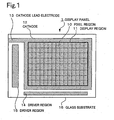
- FIG. 1 is an overall drawing of a display panel comprising an active matrix panel; comprising EL elements.
- the display panel 1 is configured by positioning a display region 11 and driver regions 14 and 15 on a glass substrate 16.
- a cathode 12 is formed over the entirety of the display region 11, and is connected to the cathode lead electrode 13.
- Pixel regions 10 are arranged in a matrix in the display region 11.
- the pixel regions 10 are configured to enable emission of primary colors (for example, the three primary colors red, blue, green) taken as necessary for color display; a combination of pixel regions emitting light of each primary color becomes one pixel element.
- the driver region 15 positioned in the column direction of the display region 11 outputs a write control line Vsel and a light emission control line Vgp; and the driver region 14 positioned in the row direction of the display region 11 outputs, in addition to the power supply line Vdd, data current signals to the data line Idata.
- driver circuits not shown, formed in the driver regions 14 and 15, an arbitrary image can be displayed in the display region 11.
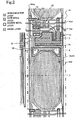
- Fig. 2 shows a plane view which explains the wiring pattern in one pixel region and the periphery.
- the patterns can be seen in the semiconductor layer 102, which is particularly important and is shown in Fig. 3, in the gate metal layer 104, source metal layer 106, and anode layer 110.
- the light-emitting portion OLED and peripheral circuitry to drive this portion are all positioned in the region enclosed by the power supply line Vdd and the data line Idata.
- the power supply line Vdd is positioned at a distance from the data line Idata, with the light-emitting portion OLED intervening.
- the peripheral circuit comprises a transistor T1 as a first active element, a transistor T2 as a second active element, a transistor T3 as a current-controlling active element, a transistor T4 as a light emission-controlling active element, and a holding capacitor C as a holding element. No restrictions in particular are placed on the conduction types of the transistors T1 to T4, but in this embodiment, the conduction type of transistor T1 is p type, and that of all the other transistors is n type.
- the source of the transistor T1 is connected to the power supply line Vdd, and the drain is connected to the drain side of transistor T4.
- the source of transistor T4 is connected to the anode of the light-emitting portion OLED.
- the holding capacitor C is formed between the power supply line Vdd and the gate of transistor T1.
- the source of transistor T2 is connected to the holding capacitor C and to the gate of transistor T1, and the drain is connected to the drain of transistor T3 and between transistors T1 and T4.
- the source of transistor T3 is connected to the data line Idata, and the gate is connected, in common with the gate of transistor T2, to the write-control line Vsel.
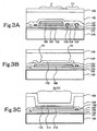
- Fig. 3 shows cross-sections to explain the layer structure in each of the cross-sectional planes shown in Fig. 2.
- Fig. 3A, Fig. 3B, and Fig. 3C show the layer structure in the A-A cross-sectional plane, B-B cross-sectional plane, and C-C cross-sectional plane, respectively.
- the pixel region 10 is configured by stacking, on the glass substrate 100 (the glass substrate 16 in Fig. 1), an underlayer protection film 101, semiconductor layer 102, gate insulating film 103, gate metal layer 104, first interlaminar insulating film 105, source metal layer 106, second interlaminar insulating film 107, bank layer 108, and cathode layer 109 (the cathode 12 in Fig. 1).
- the electric field light-emitting portion OLED is configured by stacking an anode layer 110, hole transport layer 111, and light-emitting layer 112.
- the EL elements of this embodiment emit light on the substrate side and it is necessary that light be transmitted
- soda lime glass, low-expansion glass, quartz glass, and other non-alkaline glasses are employed.
- an optically transmissive material is used as the cathode layer 109 and EL elements are configured such that light is emitted from the cathode side
- metal or other conductive materials as well as silicon carbide (SiC), alumina (Al 2 O 3 ), aluminum nitride (AIN), and other non-transparent insulating materials.
- the underlayer protective film 101 silicon oxide film (SiO x ; 0 ⁇ x ⁇ 2), silicon nitride film (Si 3 N x : 0 ⁇ x ⁇ 4), and other insulating materials can be used.
- the underlayer protective film is formed in order to prevent sodium (Na) and other mobile ions contained in the glass substrate from penetrating into the semiconductor layer and exerting adverse effects on impurity control in the semiconductor layer.
- the underlayer protection layer 101 is formed on the substrate by atmospheric-pressure chemical vapor deposition (APCVD), low-pressure chemical vapor deposition (LPCVD), plasma-enhanced chemical vapor deposition (PECVD), or another CVD method, or by sputtering.
- APCVD atmospheric-pressure chemical vapor deposition
- LPCVD low-pressure chemical vapor deposition
- PECVD plasma-enhanced chemical vapor deposition
- CVD chemical vapor deposition
- a group IV element such as silicon germanium (Si x Ge 1-x : 0 ⁇ x ⁇ 1 ), silicon carbide (Si x C 1-x : 0 ⁇ x ⁇ 1), or germanium carbide (Ge x C 1-x : 0 ⁇ x ⁇ 1),
- the semiconductor layer 102 is formed by first depositing silicon or similar by, for example, the APCVD, LPCVD, PECVD or other CVD method, or by sputtering, evaporation deposition, or other PVD method, and then irradiating with laser light to induce a polycrystalline structure.
- laser light the fundamental and higher harmonics of an excimer laser, argon ion laser, or YAG laser are used as appropriate.
- This polycrystalline semiconductor layer 102 is patterned so as to be compatible with the element shapes of the holding capacitance C and each of the TFTs (thin film transistors) T1 to T4.
- a semiconductor layer in an amorphous state can be patterned into an island morphology compatible with element shapes.
- a gate metal layer is formed, and then the gate metal layer is used as a mask to introduce impurities into the semiconductor layer.
- phosphorus (P), arsenic (As), antimony (Sb), or other donor elements are added for each element to obtain n-type semiconductor layer, and boron (B), aluminum (Al), gallium (Ga), indium (In), and other acceptor elements are added to obtain p-type semiconductor layer.
- impurities are introduced such that the semiconductor layer constituting the holding capacitor C are n-type semiconductor layer.
- TFTs with an LDD structure are employed and the threshold voltage of the TFTs is to be adjusted, channel doping to introduce impurities in low concentrations is performed.
- a silicon dioxide film is formed using tetraethyl orthosilicate (TEOS) as the raw material.
- TEOS tetraethyl orthosilicate
- the gate insulating film 103 is formed by, for example, plasma CVD in a microwave-discharge plasma, ECR plasma, or other oxygen or nitrogen atmosphere.
- a conductive material such as, for example, tantalum (Ta), tungsten (W), chromium (Cr), or aluminum (Al) is used.
- the gate metal layer 104 is formed by first depositing a film by sputtering or other means, and then patterning into the shape of a gate electrode.
- the first interlaminar insulating film 105 silicon oxide, silicon nitride, or some other insulating film can be used.
- the first interlaminar insulating film is formed by sputtering or similar, and, for example, contact holes are then formed in order to form TFT source and drain electrodes.
- the source metal layer 106 in addition to aluminum (Al), for example, tantalum, molybdenum, titanium, tungsten, or some other conductive material can be used.
- the source metal layer is formed by using sputtering or another method to uniformly layer a conductive material, and then patterning according to the electrode shape.
- the second interlaminar insulating film 107 silicon oxide, silicon nitride, or some other insulating film can be used.
- the second interlaminar insulating film is formed by sputtering or other means, and then, for example, contact holes h1 and h2 for the anode layer 110 are formed.
- anode layer 110 for example, indium tin oxide (ITO) alloy or some other optically transmissive conducting material can be used.
- ITO indium tin oxide
- NESA tin oxide
- gold, silver, platinum, copper, or another material can be used as the anode layer.
- patterning is performed according to the shape of the light-emitting portion OLED. No restrictions in particular are placed on the shape of the anode layer (or the pixel electrodes), but it is desirable that the area be larger than that of the light-emitting portion OLED.
- a contact region for electrical connection of a peripheral circuit or pixel circuit with the pixel electrodes can be provided in a region other than the light-emitting portion of the pixel electrodes.
- the flatness of, at least, the light-emitting portion can be improved.
- the bank layer 108 silicon oxide, silicon nitride, polyimide, or some other insulating material can be employed.
- the bank layer is formed by deposition using sputtering or a similar method, after which an aperture portion is provided in a position corresponding to the light-emitting portion OLED.
- the hole transport layer 111 for example, N, N'-diphenyl-N,N'-bis-(3-methylphenyl)-(1,1'-biphenyl)-4,4'-diamine (TPDA) is used.
- TPDA N, N'-diphenyl-N,N'-bis-(3-methylphenyl)-(1,1'-biphenyl)-4,4'-diamine
- the hole transport layer is deposited in the aperture portion provided in the bank layer 109, using a metal mask or similar.
- the light-emitting layer 112 for example, tris-(8-quinolinol) aluminum (Alq 3 ) or another arbitrary light-emitting material is used.
- the light-emitting layer can be formed by evaporation deposition using a metal mask or silicon mask; however, an ink jet method may be employed to arrange a solvent comprising the light-emitting material in the aperture portion, after which the solvent component is caused to evaporate.
- the cathode layer 109 a material the energy level of which enables use as the cathode of an EL element, such as aluminum or an alloy of aluminum with another element (such as lithium), or calcium or similar, is used.
- the cathode layer is formed using a metal mask or similar, and is patterned by photolithography or using a shadow mask method.
- pixel electrodes are anodes and the common electrode is a cathode; however, a configuration may be employed in which the pixel electrodes are cathodes and the common electrode is a anode.
- cathode materials are often metals, but when the pixel electrodes are cathodes, the light emitted by the light-emitting portion OLED is then emitted on the side opposite the substrate 100.
- the pixel electrodes are anodes and the common electrode is a cathode, by using a transparent material as the cathode material, or by making the film thickness sufficiently thin that light is transmitted, light can be emitted on the side opposite the substrate 100.
- One method of manufacture of EL elements involves using an ink jet method to discharge a liquid material comprising a light-emitting material, carrier transport material or carrier blocking material into an aperture portion, followed by drying, to form the light-emission layer.
- a liquid material comprising a light-emitting material, carrier transport material or carrier blocking material into an aperture portion, followed by drying, to form the light-emission layer.
- the planar shape of the aperture portion is square, then under the influence of the surface tension and viscosity of the liquid material, the height of the surface of the liquid material discharged into the corners of the aperture portion will differ from other areas. Hence there is the possibility that for a light-emitting portion with such a shape, the thickness of the light-emitting layer after film formation will be uneven.
- the boundaries of the light-emitting portion are formed so as to have at least a prescribed curvature, and at least a portion of the peripheral circuit is formed in the region surrounded by these boundaries having the prescribed curvature and the boundaries of a polygon circumscribing the boundaries of this light-emitting portion.
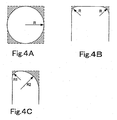
- Figs. 4A, 4B and 4C show, partially or entirely, the planar shape of a light-emitting portion to which the concept of this invention is applied.
- Fig. 4A is the case in which the boundary of the light-emitting portion is circular, that is, the entire boundary has a fixed curvature R.
- a portion of the peripheral circuit is provided within the region, indicated by shading, enclosed by this circle and by a polygon circumscribing the circle, that is, the square shown by a broken line.
- the light-emitting portion of this circle is regarded as having an ideal shape for rendering uniform the film thickness of the light-emitting portion, insofar as the shape is symmetrical about any center line passing through the center.
- effective utilization of the shaded portion is necessary in order to improve the aperture ratio of the light-emitting portion.
- Fig. 4B is an example in which this invention is applied to the corners of a rectangular shape; in this example, the boundaries of the light-emitting portion are provided with a fixed curvature R.
- the circumscribing polygon is a rectangle, shown by a broken line; the shaded regions surrounded by the boundaries of the light-emitting portion and the boundaries of the rectangle are the regions in which a portion of, or the entirety of, the peripheral circuit is provided.
- the present embodiment pertains to this example; as the curvature R is increased, an oblong planar shape for the light-emitting portion results, such as in this embodiment.
- the shape is symmetrical laterally and vertically about a center line passing through the center of the light-emitting portion, and moreover the curvature of the corner portions is equal to or greater than a fixed value, so that a light-emitting portion with uniform film thickness can be formed.
- Fig. 4C is an example in which the curvature of the corner portions is set to be unequal with respect to a center line.
- the curvature R1 of the corner portion on the left side facing the drawing is smaller than the curvature R2 of the corner portion on the right side.
- the circumscribing polygon is a rectangle, shown by a broken line, and the shaded regions surrounded by the boundaries of the light-emitting portion and the boundaries of the rectangle are regions in which a portion of or the entirety of the peripheral circuit is provided.
- the curvature is unequal in this way, by setting the minimum curvature to be greater than or equal to a constant value, a light-emitting portion with uniform film thickness can be formed. Because the minimum curvature is affected by the viscosity and surface tension of the discharged solution, and by the water repellence or liquid repellence (affinity to water or to liquids) of the discharge surface, the minimum curvature should be determined by experiment for each set of conditions.
- a light-emitting portion with a rectangular planar shape such as shown in Fig. 2, is adopted.
- a portion of the peripheral circuit namely, the contact holes h1 and h2 (see Fig. 3B) is formed within the region surrounded by the boundaries of the light-emitting layer and the boundaries of the rectangle (not shown) circumscribing the boundaries of the light-emitting portion.
- the regions indicated by shading in Fig. 4B which normally are wasted space are used for these contact holes, and this satisfy demands for effective use of space.
- any other elements of the peripheral circuit such as for example transistors and capacitors, may be formed in the regions surrounded by the boundaries of the light-emitting portion and the boundaries of a polygon circumscribing the light-emitting portion.
- a curvature can be represented as a collection of fine straight lines, and so the shape of the light-emitting portion can be interpreted as a polygon having more numerous vertices than the shape of the pixel electrode.
- provision of a contact hole in a region surrounded by the boundaries of the light-emitting portion and the boundaries of a polygon circumscribing the light-emitting portion, as shown in Fig. 2, is significant.
- the region can be used effectively, and sufficient current can be supplied to the light-emitting portion.
- a plurality of contact holes be provided. That is, in the EL element, a certain amount of current in the light-emitting layer must be passed uniformly to the entirety of the light-emitting portion. If a contact hole used for connection to an anode directly supplying current is provided in an eccentric position, the supply of current may be uneven. An uneven supply of current appears as irregularities in the intensity of light emission.
- a plurality of contact holes are provided in positions which are symmetrical with respect to a center line passing through the center of the light-emitting portion, then this problem can be resolved. That is, as shown in Fig. 2, in this embodiment a plurality of comparatively large contact holes are provided in regions provided symmetrically with respect to a prescribed center line passing through the center of the light-emitting portion.
- the stability of the current supplied to the light-emitting portion may be affected by fluctuations in the holding capacitance.
- shifts in position give rise to fluctuations or scattering in capacitance values, and there are cases in which capacitance values of holding capacitances may cause fluctuations either among pixel regions, or among display panels.
- the occupied region or width of a layer positioned on the lower side is formed to be larger than the occupied region or width of the layer positioned on the upper side (relative to the semiconductor layer, the gate metal layer and source metal layer; relative to the gate metal layer, the source metal layer).
- EL elements comprise a common electrode; the common electrode is formed over the entirety of the display region.
- a cathode 13 (cathode layer 109) is formed over the entirety of the display region 11 as shown in Fig. 1 as the common electrode for the light-emitting portion OLED.
- the common electrode is formed over the entirety, there is the problem that a capacitance occurs with the gate metal layer connected to the gates of transistors. If such stray capacitance appears, lags occur in transistor operation, and operation with the timing of the design cannot be guaranteed.
- the wiring pattern formed by the gate metal layer is positioned with a separation of at least a prescribed distance from at least one among the electrodes of the light-emitting layer.
- a problem due to low impedance arises due to the distance between the cathode layer 109 which is the common electrode and the gate metal layer 104.
- the cathode layer 109 is a small distance from the lower side in the light-emitting portion OLED, so that the distance from the gate metal layer in the vicinity of the light-emitting portion poses a problem.
- Fig. 7 (equivalent to the C-C cross-section in Fig. 2), patterns are formed such that, near the light-emitting portion, the distance d1 in the depth direction between the cathode layer 109 and the gate metal layer 104 and the distance d2 in the plane are both equal to or greater than a prescribed distance.
- the prescribed distance will change variously depending on the area of the gate metal layer and the dielectric constants of intervening layers, and so cannot be specified generally; however, it is preferable that patterning should be at as great a distance as possible, within the range allowed by the area of pixel regions and other.
- the data lines Idata and scan lines Vsel use the gate metal layer 104 which is at a greater distance from the cathode 109 which is a common electrode, and at the intersections between data lines Idata and scan lines Vsel, data lines Idata are formed in the source metal layer 106, but the portions of data lines Idata outside intersections and the scan lines Vsel are formed in the gate metal layer 104.
- the entirety of the data lines Idata may be formed in the conducting layer which is at the greatest distance from the common electrode.
- scan lines Vsel are formed in the source metal layer 106, and the entirety of data lines Idata as well as the portion of scan lines Vsel outside intersections may be formed in the gate metal layer 104.
- a conducting layer may be formed in the same layer as the semiconductor layer 102; and, if a so-called bottom-gate configuration for transistors is employed, then the conducting layer may be provided below the semiconductor layer, and this conducting layer can be used for wiring of signal lines.
- Fig. 5 shows a circuit diagram for one pixel circuit constituting the pixel region 10.
- transistor T2 which is an active element directly connected to the holding capacitor C is an active element with multiple control terminals, that is, a multi-gate type transistor.
- a transistor as indicated by the arrow in Fig. 5, is for practical purposes equivalent to directly connecting a plurality of transistors, and the leakage current is greatly suppressed. A current corresponding to the supplied data signal is reliably supplied to the light-emitting portion OLED.
- an LDD, GDD, or ODD structure can also be employed.
- the leakage current can be reduced, and adverse effects due to hot electrons when a FET is miniaturized are suppressed, so that element reliability is enhanced.
- transistor T1 and transistor T2 have opposite polarities, that is, transistor T1 is a p-type FET, and transistors T2 to T4 are n-type FETs.
- transistor T1 is a p-type FET
- transistors T2 to T4 are n-type FETs.
- whether to use a p-type or an n-type [transistor can be decided arbitrarily according to the polarity and other details of signals which are to be used, and no restrictions apply.
- the placement of elements is not limited to that of Fig. 5.
- the electrical potential relationships of the holding capacitor, transistor T1, and light-emitting portion OLED can be reversed.
- the common electrode of the light-emitting portion be an anode, and that the polarities of each of the transistors (whether n-type or p-type) be reversed.
- a wiring pattern is formed such that at least one active element among the plurality of transistors and other active elements is connected to another active element by the same contact hole.
- transistors T2, T3, and T4 are interconnected by the same contact hole h3.
- the layout is optimized such that there are more numerous common connection points or contacts in a circuit, and by arranging elements such that portions which are common contact points are connected by the same connection points, the number of contact holes can be reduced and the area occupied by the peripheral circuitry is reduced due to these contact holes.
- Fig. 8 shows a plane view explaining one pixel region and the wiring pattern in the vicinity thereof for an EL element of embodiment 2 of this invention.
- Fig. 9 shows cross-sectional views which explain the layer structure in cross-sections of Fig. 8.
- Fig. 9A shows the layer structure in a cross-section along the A-A plane
- Fig. 9B is a cross-section along B-B
- Fig. 9C is a cross-section along C-C.
- the patterns of the principal semiconductor layer 102, gate metal layer 104, source metal layer 106, and anode layer 110 are shown.
- the configuration of the EL element in embodiment 2 is, except for the existence of an affinity-controlling film 113 which forms a step shape, similar to the EL element of embodiment 1. Hence components similar to those of embodiment 1 are assigned the same symbols in the drawings, and explanations are omitted.
- the light-emitting portion OLED in embodiment 2 comprises an affinity-controlling layer 113, between the second interlaminar insulating film 107 and the bank layer 108.
- This affinity-controlling layer 113 need not be formed over the entire pixel region, but when forming a light-emitting portion OLED using a liquid material, should preferably be provided at least near the boundaries of the light-emitting portion.
- the affinity-controlling layer 113 must have an affinity for the liquid material used in forming the light-emitting portion.
- the bank layer 108 forms a wall near the boundary of the light-emitting portion; a material is selected which exhibits no affinity for the liquid material used when forming the light-emitting layer 110, and [the bank layer] is stacked on top of the affinity-controlling layer 113. Consequently the affinity-controlling layer 113 forms a step shape Step on the inside of the light-emitting portion in the wall formed by the bank layer, as shown in Fig. 8 and Fig. 9C.
- the material of the affinity-controlling layer 113 is determined according to the kind of properties of the liquid material which is used to fill the light-emitting region by the ink jet method. For example, if the liquid material comprises a liquid such as water which is highly polar, it is desirable that the affinity-controlling layer have polar bases, at least in the portion making contact with the liquid material or on the surface. Conversely, if the liquid material comprises a nonpolar liquid, it is desirable that the affinity-controlling layer have nonpolar bases, at least in the portion making contact with the liquid material or on the surface. Also, the extent of the affinity of the affinity-controlling layer is determined by the surface tension of the liquid material which fills the light-emitting region.
- the affinity-controlling layer even if a material which chemically has a weak affinity for water is used as an affinity-controlling layer, if the liquid material comprises large quantities of a solvent with a surface tension lower than that of water, the surface tension of the liquid material will be lower than that of water, and so the affinity-controlling layer will exhibit affinity for the liquid.
- the type of material to use in the affinity-controlling layer is changed variously according to the liquid material to be used.
- the affinity-controlling layer 113 comprise an inorganic compound or organic compound which in turn comprises one among Al, Ta or another metal, silicon oxide, silicon nitride, amorphous silicon, polysilicon, polyimide, an organic compound with fluoride bonds, or a photoresist. If insulating properties are necessary, the affinity-controlling layer comprises a nonmetallic compound.
- the affinity of these materials is determined by differences in the contact angle with respect to the liquid material. That is, the degree of affinity or absence of affinity is determined in relative and not absolute terms. The degree of affinity can also be adjusted through surface treatment methods.
- the bank layer 108 comprise a material with weaker affinity than the affinity-controlling layer 113. This is because, by making the affinity of the bank layer weaker than that of the affinity-controlling layer, the absence of affinity of the bank layer can repel the liquid material to prevent flowing of the liquid material into neighboring pixel regions and avoid short-circuits. Also, the absence of affinity of the bank layer prevents liquid material from being drawn excessively toward the bank layer side so that a concave-shape film is formed.
- an affinity-controlling layer with an affinity for the liquid material is provided near the boundaries of the light-emitting portion, so that a light-emitting layer of uniform film thickness can be formed.
- an affinity-controlling layer with affinity for the liquid material is provided near the boundaries of the light-emitting portion, so that the uniformity of the thickness of the hole injection layer, light-emitting layer, and other layers constituting the light-emitting portion is improved.
- the affinity-controlling layer 113 is formed in a step shape; but when the thickness of the layer cross-section can be made sufficiently great, walls without a step shape, that is, a single wall without a step with the bank layer, may be formed.
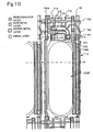
- Fig. 10 shows a plane view which explains one pixel region and the peripheral wiring pattern for an EL element in embodiment 3.
- Fig. 11 shows cross-sectional views explaining the layer structure in cross-sections indicated in Fig. 10.
- Fig. 11A and Fig. 11B show the layer structures in the cross-sections along A-A and B-B respectively in Fig. 10.
- patterns in the principal semiconductor layer 202, gate metal layer 204, source metal layer 206, and anode layer 210 can be seen.
- the width of the pixel region 20 is smaller than the width of the pixel region 10 in embodiment 1.
- the circuit configuration is similar to that of embodiment 1 (see Fig. 5), and the materials forming each layer are also similar to embodiment 1, and so components which are the same as in embodiment 1 are assigned the same symbols in the drawings, and explanations are omitted.
- the glass substrate 100, underlayer protection film 101, semiconductor layer 102, gate insulating film 103, gate metal layer 104, first interlaminar insulating film 105, source metal layer 106, second interlaminar insulating film 107, bank layer 108, cathode layer 109, anode layer 110, hole transport layer 111, and light-emitting layer 112 in embodiment 1 correspond, respectively, to the glass substrate 200, underlayer protection film 201, semiconductor layer 202, gate insulating film 203, gate metal layer 204, first interlaminar insulating film 205, source metal layer 206, second interlaminar insulating film 207, bank layer 208, cathode layer 209, anode layer 210, hole transport layer 211, and light-emitting layer 212 in embodiment 3.
- the transistors T1 to T4 in embodiment 1 correspond respectively to the transistors T11 to T14 in embodiment 3
- the contact holes h1 to h3 in embodiment 1 correspond respectively to the contact holes h11 to
- the holding capacitor C was positioned between the power supply line Vdd and the data line Idata, outside the light-emitting portion (in the upper portion of the light-emitting portion in Fig. 2).
- the area of the pixel region is comparatively small as in this embodiment, that is, when the pixel density is high, it is not possible to secure sufficient element space for occupation by the holding capacitor.
- the holding capacitor C is formed in the region in which at least one among a first metal layer (for example, the source metal layer 206) or a second layer forms a power supply wiring pattern.
- the holding capacitor C is formed by stacking a gate metal layer 204 in parallel below the power supply line Vdd (source metal layer 206) positioned on the side of the light-emitting portion OLED.
- the holding capacitor C is formed by causing an overlapping region to occur among the plurality of layers (for example, the source metal layer 206, gate metal layer 204, and semiconductor layer 202) relating to formation of the holding capacitor C, similarly to the holding capacitor explained in embodiment 1; near the overlapping region in which the holding capacitor C is formed, the region occupied by the layer positioned on the lower side among the plurality of layers is formed to be larger than the region occupied by layers positioned on the upper side.
- the width of the source metal layer 206 is d11
- the width of the gate metal layer 204 is d12
- the width of the semiconductor layer 202 is d13
- the relation d13 > d12 > d11 obtains. The lower the layer, the larger the pattern shape is made.
- the extent to which the size is increased will depend on the precision of the manufacturing processes and the pattern density. As one approach, patterns should be formed for each layer such that, when forming layers positioned on the upper side, even when the maximum possible shift in position occurs, the region in the layer positioned on the upper side will be contained within the region in the layer positioned on the lower side. In this embodiment also, the differences d13-d12 and d12-d11 are designed to be equal to or greater than predicted position shifts in manufacturing processes.
- the above-described holding capacitor be formed below the bank layer 208, in order to isolate the above-described neighboring light-emitting portion. That is, because the bank layer is necessary for pixel separation, by superposing the wiring region for the power supply line and the overlapping region for the holding capacitor, the area occupied by the peripheral circuit can be greatly reduced, and a sufficient aperture ratio can be secured.
- a wiring pattern is fabricated such that at least one active element among a plurality of transistors and other active elements is connected to another active element by the same contact hole.
- the transistors T12, T13 and T14 are interconnected by the same contact hole h13.
- Fig. 12 shows a plane view which explains one pixel region and the peripheral wiring pattern for an EL element in embodiment 3 of this invention.
- Fig. 13 shows cross-sectional views which explain the layer structure at cross-sections indicated in Fig. 12.
- Fig. 13A and, Fig. 138 show the layer structure at cross-sections A-A and B-B respectively in Fig. 12.
- the patterns of the principal semiconductor layer 202, gate metal layer 204, source metal layer 206, and anode layer 210 can be seen.
- the light-emitting portion OLED in embodiment 4 comprises an affinity-controlling layer 213 between the second interlaminar insulating film 207 and the bank layer 208.
- This affinity-controlling layer 213 need not be formed over the entire pixel region, but must be provided, at least, near the boundaries of the light-emitting portion.
- the affinity-controlling layer 213 must have affinity with the liquid material used in forming the light-emitting portion.
- the bank layer 208 forms walls near the boundaries of the light-emitting portion; a material which exhibits a lack of affinity with the liquid material used when forming the light-emitting layer 212 or hole injection layer 211 is selected, and is stacked on top of the affinity-controlling layer 213. Consequently the affinity-controlling layer 213 forms a step shape on the inside of the light-emitting portion with respect to the wall formed by the bank layer, as shown in Fig. 12 and Fig. 13B.
- the material of the affinity-controlling layer 113 is determined according to the properties of the liquid material with which the light-emitting region is filled using the ink jet method. For example, if the liquid material comprises a liquid such as water which is highly polar, it is desirable that the affinity-controlling layer have polar bases, at least in the portion making contact with the liquid material or on the surface. Conversely, if the liquid material comprises a nonpolar liquid, it is desirable that the affinity-controlling layer have nonpolar bases, at least in the portion making contact with the liquid material or on the surface. Also, the extent of the affinity of the affinity-controlling layer is determined by the surface tension of the liquid material which fills the light-emitting region.
- the affinity-controlling layer even if a material which chemically has a weak affinity for water is used as an affinity-controlling layer, if the liquid material comprises large quantities of a solvent with a surface tension lower than that of water, the surface tension of the liquid material will be lower than that of water, and so the affinity-controlling layer will exhibit affinity for the liquid.
- the type of material to use in the affinity-controlling layer is changed variously according to the liquid material to be used.
- the affinity-controlling layer 213 comprise an inorganic compound or organic compound which in turn comprises one among Al, Ta or another metal, silicon oxide, silicon nitride, amorphous silicon, polysilicon, polyimide, an organic compound with fluoride bonds, or a photoresist. If insulating properties are necessary, the affinity-controlling layer comprises a nonmetallic compound.
- the affinity of these materials is determined by differences in the contact angle with respect to the liquid material. That is, the degree of affinity or absence of affinity is determined in relative and not absolute terms. The degree of affinity can also be adjusted through surface treatment methods.
- the bank layer 108 comprise a material with weaker affinity than the affinity-controlling layer 113. This is because, by making the affinity of the bank layer weaker than that of the affinity-controlling layer, the absence of affinity of the bank layer can repel the liquid material to prevent flowing of the liquid material into neighboring pixel regions and avoid short-circuits. Also, the absence of affinity of the bank layer prevents liquid material from being drawn excessively toward the bank layer side so that a concave-shape film is formed.
- an affinity-controlling layer with an affinity for the liquid material is provided near the boundaries of the light-emitting portion, so that the uniformity of the thickness of the hole injection layer, light-emitting layer, and other layers constituting the light-emitting portion can be improved.
- a bank layer forming a wall near the boundaries of the light-emitting portion exhibits a lack of affinity with the liquid material, so that short-circuits with the neighboring pixel regions can be prevented.
- the affinity-controlling layer 213 is formed in a step shape; but when the thickness of the layer cross-section can be made sufficiently great, walls without a step shape, that is, a single wall without a step with the bank layer, may be formed.
- This embodiment relates to a display panel which is an electro-optical device having EL elements which are electro-optical elements explained in the above embodiments, and electronic device comprising such a display panel,
- Fig. 14 shows a connection diagram for a display panel 1 of this embodiment.
- pixel regions are arranged in the display region 11.
- the pixel regions 10 of embodiment 1 or embodiment 2, or the pixel regions 20 of embodiments 3 or 4 may be employed.
- Control signals are supplied to each pixel region from the driver region 14, via the light-emission control lines Vgp and write-control lines Vsel.
- Data signals and a power supply voltage are supplied to each pixel region from the driver region 15, via data lines Idata and power supply lines Vdd.
- the display panel 1 of this embodiment can be employed in various electronic device.
- Fig. 15 shows examples of electronic device which can employ the display panel 1.
- Fig. 15A is an example of application to a portable telephone set; the portable telephone 30 comprises an antenna portion 31, voice output portion 32, voice input. portion 33, operation portion 34, and a display panel 1 of this invention.
- a display panel of this invention can be utilized as the display portion.
- Fig. 15B is an example of application to a camcorder; the camcorder 40 comprises an imaging portion 41, operation portion 42, audio input portion 43, and a display panel 1 of this invention.
- a display panel of this invention can be utilized as a viewfinder or display portion.
- Fig. 15C is an example of application to a portable personal computer; the computer 50 comprises a camera portion 51, operation portion 52, and a display panel 1 of this invention.
- a display panel of this invention can be utilized as a display portion.
- Fig. 15D is an example of application to a head-mounted display; the head-mounted display 60 comprises a band 61, optical system housing portion 62, and a display panel 1 of this invention.
- a display panel of this invention can be utilized as an image display source.
- Fig. 15E is an example of application to a rear projector; the projector 70 comprises a housing 71, light source 72, synthetic optical system 73, mirror 74, mirror 75, screen 76, and a display panel 1 of this invention.
- a display panel of this invention can be utilized as an image display source.
- Fig. 15F is an example of application to a front projector; the projector 80 comprises a housing 82, optical system 81, and a display panel 1 of this invention, and is capable of displaying images on a screen 83.
- a display panel of this invention can be utilized as an image display source.
- Electro-optical devices of this invention are not limited to the above examples, but extend to all electronic device to which active-matrix type display devices can be applied.
- utilization in fax machines with display functions, in the viewfinders of digital cameras, in portable TV sets, in DSP devices, in PDAs, in electronic organizers, in electro-optical bulletin boards, in displays for advertising and announcements, and in other areas is possible.
Landscapes
- Engineering & Computer Science (AREA)
- Physics & Mathematics (AREA)
- Microelectronics & Electronic Packaging (AREA)
- Geometry (AREA)
- General Physics & Mathematics (AREA)
- Theoretical Computer Science (AREA)
- Computer Hardware Design (AREA)
- Nonlinear Science (AREA)
- Mathematical Physics (AREA)
- Optics & Photonics (AREA)
- Crystallography & Structural Chemistry (AREA)
- Chemical & Material Sciences (AREA)
- Devices For Indicating Variable Information By Combining Individual Elements (AREA)
- Electroluminescent Light Sources (AREA)
- Control Of Indicators Other Than Cathode Ray Tubes (AREA)
- Thin Film Transistor (AREA)
- Control Of El Displays (AREA)
Abstract
An active matrix substrate is provided which does not cause reductions in the brightness of electroluminescence elements, and which comprises appropriate peripheral circuitry occupying a small area. The active matrix substrate comprises peripheral circuits to supply current to EL elements provided for each pixel, and corresponding to EL elements, and further comprises a holding element (C) which holds a control voltage, a first active element (T1) connected to the holding element (C) and which supplies current to a light-emitting portion (OLED) based on a control voltage, and a second active element (T2) connected to the holding element (C) and which controls the charging and discharging of the holding element. In particular, the second active element (T2) is configured as a multiple-control-terminal type active element. As a result; there are no fluctuations in the programmed current. <IMAGE>
Description
This invention relates to an active matrix substrate suitable for electro-optical
devices, an electro-optical device, and electronic device.
The active matrix driving method is one method of driving electro-optical
devices comprising liquid crystal elements, organic electroluminescence (EL)
elements, electrophoretic elements, electronic emission elements, and similar. In an
electro-optical device driven by the active matrix driving method, a plurality of pixels
are arranged in a matrix on the display panel. Each of the plurality of pixels
comprises a pixel circuit, in turn comprising an electro-optical element and a driving
transistor which supplies driving power to the electro-optical element. Each of the
plurality of pixel circuits is arranged to correspond to the intersection of a data line
and a scan line (see, for example, patent reference 1: Internationally disclosed
pamphlet no. WO98/36407).
In order to precisely control brightness in an electro-optical device, the
amount of power supplied to electro-optical elements must be precisely controlled.
In particular, because organic EL elements are current-driving type electro-optical
elements, the brightness is directly affected by the current. Hence there is a need to
precisely supply the desired current to organic EL elements; and in addition to
optimizing the driving circuit and driving method, the pixel layout must also be
optimized. Problems encountered in actual pixel layouts include, for example,
contact between pixel electrodes and peripheral circuitry, stability of holding
capacitances, and transistor turn-off currents.
The present invention was devised in light of the above circumstances, and
has as an object the provision of an active matrix substrate, electro-optical device,
and electronic device comprising an optimal pixel layout for the stable driving of
electro-optical elements.
In order to resolve the above problems, a first active matrix substrate of this
invention is an active matrix substrate comprising peripheral circuitry to supply a
current to electro-optical elements provided in each pixel according to the electro-optical
element; each peripheral circuit comprises a holding element to hold a
control voltage, a first active element, connected to the holding element, to supply a
current to the electro-optical element based on the control voltage, and a second
active element, connected to the holding element, to control the charging and
discharging of the holding element; and the above second active element has a
structure which prevents leakage currents during shutoff.
Here "electro-optical element" refers to general elements which emit light, or
change a status of light in response to external light, due to electrical action, and
comprises both elements which themselves emit light, and elements which control
the transmission of external light. For example, electro-optical elements include
liquid crystal elements, electrophoretic elements, EL elements, and electron
emission elements which emit light by causing electrons generated through
application of an electric field to strike an emission plate.
"Peripheral circuits" refers to the aggregation of circuit elements which drive
each pixel in an active-matrix type electro-optical device, and comprises, for
example, TFTs (thin film transistors) or similar.
"Active matrix substrate" refers to general substrates on which is mounted
peripheral circuitry, regardless of whether electro-optical elements are formed or not.
There is no particular restriction on "active elements", which may include, for
example, TFTs and other transistors and diodes, or similar.
Here "holding element" refers to, for example, capacitors, memory, and other
elements which hold electrical signals.
Normally, when an active element is in the non-conducting state, whereas
ideally there should be no current flowing, a current, albeit slight, may flow; an
active element having a "structure to prevent leakage currents during shutoff" refers
to an active element configured with the object of preventing the occurrence of such
a current (leakage current).
An example of such an element is a multi-gate type active element. A multi-gate
type active element is an active element which functions as a single element,
but strictly speaking comprises a plurality of active elements connected in series,
configured to function similarly to a device with control terminals connected together.
In configuring a multi-gate type active element, the semiconductor layer may
be in a curved shape, as in an embodiment described below, or the gate shape may
be curved.
The second active element may be a transistor with a structure selected from
the group consisting of an LDD structure, GDD structure, or DDD structure. Here
"LDD" is an abbreviation of "Lightly Doped Drain"; "GDD" is an abbreviation of
"Graded Diffused Drain"; and "DDD" is an abbreviation of "Double Diffused Drain".
In a transistor having these structures, in order to limit the adverse effects of hot
electrons and similar during fine MOSFET fabrication, the maximum electric field
near the drain is weakened. For example, in such transistors the drain region of the
transistor is lightly doped with impurities to relax the electric field in regions where
impurity diffusion is performed and between silicon substrates; for example, n-type
regions may be formed using self-alignment.
In such transistors, because the source-drain resistance while the transistor
is turned off is extremely high and leakage currents are reduced, electric charge
accumulated in the holding element is not released, and the electric potential
applied to a control terminal can be maintained at a constant level.
A second active matrix substrate of this invention is an active matrix substrate
comprising a plurality of unit circuits, arranged to correspond to the intersections of
a plurality of data lines and a plurality of scan lines. Each of the above plurality of
unit circuits comprises a first transistor, which comprises a first control terminal, first
terminal, and second terminal; a holding element, connected to the above first
control terminal, comprising a first electrode and a second electrode; and a second
transistor, comprising a third terminal, a fourth terminal, and a second control
terminal, wherein the above third terminal and the above fourth terminal are
respectively connected to the above first terminal and to the above first electrode;
and the above second transistor has a multi-gate structure.
In the above active matrix substrate, in place of a multi-gate structure, the
above second transistor may be a transistor with a structure selected from an LDD
structure, GDD structure, or DDD structure.
By adopting a multi-gate structure and an LDD structure, GDD structure, or
DDD structure, the leakage current when the second transistor is in the turned-off
state can be reduced, so that the electric charge accumulated in the holding
element can be maintained for a long period of time.
In the above active matrix substrate, it is preferable that the above first
transistor and the above second transistor have different conduction types. In this
case, it is preferable that the semiconductor film constituting the above first
transistor and the semiconductor film constituting the above second transistor be
separated.
For example, it is preferable that the above first transistor by p-type, and that
the above second transistor be n-type.
The above active matrix substrate may further comprise a third transistor,
comprising a fifth terminal, a sixth terminal, and a third control terminal, with the
above third control terminal connected to one scan line among the above plurality of
scan lines, and the above fifth terminal connected to one data line among the above
plurality of data lines.
The above sixth terminal may be connected to the above third terminal and to
the above first terminal.
In the above active matrix substrate, the above active matrix substrate may
have a stacked-layer structure comprising a plurality of layers; the above plurality of
layers may comprise a semiconductor layer, in which is formed a semiconductor film
constituting the above first and second transistors, and a gate metal layer, in which
are formed the above second control terminals; and in the above gate metal layer
there may be formed at least one portion of at least one scan line among the above
plurality of scan lines.
By this means, the above second control terminal and at least one portion of
the scan line can be formed in the same process, so that manufacturing processes
can be shortened.
In the above active matrix substrate, the above active matrix substrate may
have a stacked-layer structure comprising a plurality of layers; the above plurality of
layers may comprise a semiconductor layer, in which is formed a semiconductor film
constituting the above first and second transistors, and a gate metal layer, in which
are formed the above second control terminals; and in the above gate metal layer
there may be formed at least one portion of at least one data line among the above
plurality of data lines.
By this means, the above second control terminal and at least one portion of
the data line can be formed in the same process, so that manufacturing processes
can be shortened.
In the above active matrix substrate, the above active matrix substrate may
have a stacked-layer structure comprising a plurality of layers; the above plurality of
layers may comprise a semiconductor layer, in which is formed a semiconductor film
constituting the above first and second transistors, a gate metal layer, in which are
formed the above second control terminals, and a source metal layer, in which is
formed a source electrode or drain electrode connected to the source or to the drain
of the above second transistor; and at least one portion of at least one data line
among the above plurality of data lines may be formed in the layer closer to the
above semiconductor layer among the above source metal layer and the above gate
metal layer.
By this means, when an electro-optical device is formed in which electro-optical
elements are arranged above the active matrix substrate, at least one portion
of a data line can be separated from the electrodes of electro-optical elements, so
that operation delays due to stray capacitances occurring between electrodes and
data lines can be reduced.
A third active matrix substrate of this invention comprises unit circuits,
comprising transistors, as well as data lines and scan lines, and has a stacked-layer
structure comprising a plurality of layers; the above plurality of layers
comprises a semiconductor layer, in which is formed a semiconductor film
constituting transistors, and a gate metal layer, in which are formed the gate
terminals of the above transistors; and at lease one portion of either the above scan
lines, or the above data lines, or both, is formed in the above gate metal layer.
By this means, transistor gate terminals and at least one portion of the scan
lines or data lines can be manufactured by the same process, so that manufacturing
processes can be shortened.
A fourth active matrix substrate of this invention comprises unit circuits,
comprising transistors, as well as data lines and scan lines, and has a stacked-layer
structure comprising a plurality of layers; the above plurality of layers
comprises a semiconductor layer, in which is formed a semiconductor film
constituting transistors, a gate metal layer, in which are formed the gate terminals of
the above transistors, and a source metal layer in which are formed the source
electrodes or drain electrodes which are connected to the sources or drains of the
above transistors; and at lease one portion of either the above scan lines, or the
above data lines, or both, is formed in the layer, among the above gate metal layer
and the above source metal layer, which is closer to the above semiconductor layer.
In the above active matrix substrate, when an electro-optical device is formed
in which electro-optical elements are arranged above the active matrix substrate, at
least one portion of data lines or scan lines can be separated from the electrodes of
electro-optical elements, so that delays in signal supply due to stray capacitances
occurring between electrodes and data lines or scan lines can be suppressed.
In the above active matrix substrate, it is preferable that a unit circuit
comprise a first transistor, comprising a first control terminal, a first terminal, and a
second terminal; a holding element, connected to the above first control terminal,
and comprising a first electrode and a second electrode; and a second transistor,
comprising a third terminal, a fourth terminal, and a second control terminal, wherein
the above third terminal and the above fourth terminal are respectively connected to
the above first terminal and to the above first electrode; and that the unit circuit have
at least a structure selected from an LDD structure, GDD structure, DDD structure,
or multi-gate structure.
The LDD structure, GDD structure, DDD structure, and multi-gate structure
are appropriate structures for suppressing current leaks, and so by employing such
a configuration, the electric charge accumulated in the holding element can be
maintained for long periods of time.
A first electro-optical device of this invention comprises the above active
matrix substrate, and electro-optical elements.
A second electro-optical device of this invention comprises peripheral
circuits to supply current to electro-optical elements provided for each pixel,
corresponding to the above electro-optical elements; each of the above peripheral
circuits comprises a light emission-controlling active element to supply current to the
above electro-optical element during the light emission period, a holding element to
hold a control voltage, a first active element the gate terminal of which is connected
to the above holding element and which supplies a current based on the above
control voltage applied to the gate terminal to the above electro-optical element, via
the above light emission-controlling active element, a current-controlling active
element which passes a constant current (or a data current) via the above first
active element during the selection period, and a second active element connected
between the above current-controlling active element and the above holding
element, which charges the above holding element during the above selection
period and which stores the above control voltage; and the above second active
element comprises a structure to prevent leakage currents during shutoff.
As the above structure to prevent leakage currents, similarly to the case of
the above active matrix substrates, for example, an LDD structure, GDD structure,
DDD structure, or multi-gate structure can be adopted.
In the above electro-optical device, as the above first active element and the
above second active element, it is preferable that, for example, a transistor be used.
in this case, it is preferable that the transistors have different conduction types. For
example, it is preferable that the above first active element be p-type, and that the
above second active element be n-type.
Corresponding to this, a configuration may be adopted comprising a first
driver circuit which supplies negative-logic data signals to the first active element,
and a second driver circuit which supplies positive-logic scan signals to the second
active element.
In the above electro-optical device, a configuration may be adopted
comprising data lines which supply data signals to first active elements, and scan
lines, intersecting the data lines, which supply scan signals to second active
elements.
In the above electro-optical device, it is preferable that either the data lines or
the scan lines be wired by means of the metal layer, among the source metal layer
and the gate metal layer which comprise the first active elements and second active
elements, which is separated from the common electrodes of the electro-optical
elements. This is because if the metal layer which is more distant from the common
electrodes is used, the stray capacitance arising between the signal lines and the
common electrodes can be reduced.
Specifically, the scan lines may for example be wired using the gate metal
layer which forms the gate terminals of the second active elements.
In the above electro-optical device, it is preferable that, among the plurality of
active elements, the plurality of active elements having the same polarity be formed
continuously and in planar fashion in the same semiconductor layer. This is because,
if the semiconductor layer is thus made continuous, the area used for wiring can be
reduced, and the aperture ratio can be increased.
At this time, connection points between a plurality of active elements having
the same polarity comprise common contact holes, and wiring is performed from
contact holes to active elements having a polarity differing from these active
elements. This is because when the polarity is different, normal wiring must be
performed. By this means, contact holes can be made common, and the area of
occupation of connection portions in the entire area of the driving circuit can be
reduced.
In one embodiment described below, a plurality of active elements having the
same polarity comprises second active elements, light emission-controlling active
elements, and current-controlling active elements; however, the present invention is
of course not limited thereto.
As the gate terminals of the above second active elements and the above
current-controlling active elements, common scan lines may be used; in this case,
with respect to common gate terminal connections, by using scan lines without
modification the wiring area can be reduced and the aperture ratio can be raised.
However, if the above second active elements and the above current-controlling
active elements are not driven with the same timing, then of course
different signal lines can be used as the respective gate terminals.
A third electro-optical device of this invention comprises electro-optical
elements, and peripheral circuitry driving the above electro-optical elements; the
above electro-optical elements are formed such that the boundaries of the electro-optical
elements have at least a prescribed curvature , and at least a portion of the
peripheral circuits is formed in the region surrounded by the boundaries having at
least the prescribed curvature and by polygonal boundaries circumscribing the
electro-optical elements.
A shape having a "prescribed curvature" is particularly effective when electro-optical
elements are formed using liquid materials; in this case, it is desirable that
the prescribed curvature be set according to the viscosity and surface tension of the
liquid material, and according to the material of the layer below the electro-optical
elements. However, even in cases where the electro-optical elements are formed by
evaporation deposition or other means without using liquid materials, there is the
advantageous result that short-circuits are prevented.
It is preferable that a plurality of boundary portions having this prescribed
curvature be formed. It is also preferable that the plurality of boundary portions thus
formed be arranged essentially symmetrically with respect to a center line passing
through the geometric center of the electro-optical element.
For example, a portion of the peripheral circuit formed in this region is a
contact hole comprised by wiring of the peripheral circuit. It is preferable that this
contact hole be of polygonal shape compatible with the shape of the region. A
contact hole comprised by the wiring of the peripheral circuit is, for example, a
contact hole which supplies current to at least one of the electrodes of the electro-optical
element. It is preferable that there be a plurality of contact holes, arranged
essentially symmetrically with respect to a center line passing through the geometric
center point of the above electro-optical element.
When using a liquid material to form electro-optical elements, by providing an
affinity-controlling layer which adjusts the affinity for the liquid material near the
boundaries of electro-optical elements, the film thickness of the functional layer
constituting the electro-optical elements can be controlled, and flatness can be
improved. Also, by making the affinity for the liquid material of, at least, the walls of
the bank layer different from that of the above affinity-controlling layer, the
effectiveness may be further increased. For example, by making the affinity for the
liquid material of the walls of the bank layer lower than that of the affinity-controlling
layer, the film formed by the liquid material no longer adheres to the walls of the
bank layer, and the flatness of the film formed by the liquid material is further
improved.
This affinity-controlling layer may be formed so as to have a staircase-shape
on the inside of the electro-optical elements with respect to the walls formed by the
bank layer.
Here a "bank" is a partition member to partition pixel regions. A bank is also
effective for securing a distance from cathodes or common electrodes and data lines,
scan lines, or other wiring which supplies signals. By securing a sufficient distance,
the parasitic capacitance is reduced, and delays when supplying signals can be
suppressed.
In general, data signals are greatly affected by stray capacitances of scan
signals, which can cause operation delays, and so a sufficient distance must be
secured between data signals and common electrodes or cathodes.
It is preferable that, in boundary portions having a prescribed curvature, at
least one of the electrodes constituting the electro-optical element be patterned
according to the shape of the boundary portion. This is because, by patterning
electrodes in a manner compatible with the curvature, at least a portion of the
peripheral circuit can be arranged more easily. For example, at least a portion of the
peripheral circuit is a contact region to enable connection between the peripheral
circuit and the above electrode.
A fourth electro-optical device of this invention comprises a light-emitting
portion, and a peripheral circuit which controls the current supplied to the above
light-emitting portion via a pixel electrode; the area of the above light-emitting
portion is smaller than the area of the above pixel electrode, and the shape of the
above light-emitting portion is different from the shape of the above pixel electrode.
A fifth electro-optical device of this invention comprises a light-emitting
portion, and a peripheral circuit which controls the current supplied to the above
light-emitting portion via a pixel electrode; the area of the above light-emitting
portion is smaller than the area of the above pixel electrode; the shape of the above
light-emitting portion is a shape having a curvature, and the shape of the above
pixel electrode is polygonal.
A sixth electro-optical device of this invention comprises a light-emitting
portion, and a peripheral circuit which controls the current supplied to the above
light-emitting portion via a pixel electrode; the area of the above light-emitting
portion is smaller than the area of the above pixel electrode; the above light-emitting
portion has a polygonal shape having n vertices (where n is an integer equal to 4 or
greater); the above pixel electrode has a polygonal shape having m vertices (where
m is an integer equal to 3 or greater); and the relation n>m obtains.
In the above electro-optical device, the light-emitting portion has a shape
having a curvature, or has a polygonal shape with four or more vertices, so that
short-circuits in the edge portions of light-emitting portion can be prevented. And
when forming light-emitting portions using a liquid material, the liquid material can
be made to extend thoroughly to the edge portions of light-emitting portions, so that
a uniform film can be formed.
In the above electro-optical device, it is preferable that the entire region of
the above light-emitting portion be formed on the above pixel electrode, and that a
contact region for connection to the above peripheral circuit and to the above pixel
electrode be provided in the portion of the above pixel electrode where the above
light-emitting portion is not formed.
A seventh electro-optical device of this invention comprises an electro-optical
element, a holding capacitance which regulates the current supplied to the above
electro-optical element, and an active element which supplies a current according to
the voltage recorded in the holding capacitance; a first electrode constituting the
holding capacitance is formed by patterning a portion of a metal layer which forms a
power supply line supplying current to the electro-optical element.
An eighth electro-optical device of this invention is configured to enable the
supply of current to an electro-optical element by an active element according to the
voltage recorded in a holding capacitance, and comprises a first metal layer
connected to a power supply, and a second metal layer patterned to comprise a
portion of a control terminal of an active element; a first electrode constituting the
holding capacitance is formed by patterning a portion of the first metal layer.
Here "layer" comprises, in addition to a metal layer, a layer which affects
formation of the holding capacitance, such as for example a semiconductor layer.
A second electrode constituting the holding capacitance is formed by
patterning a portion of the metal layer which forms the control terminal of the active
element.
In the above electro-optical device, the above first electrode may be a portion
of the power supply line, and a portion of the metal layer forming the control terminal
of the active element in a portion of the power supply line may be overlapped in
patterning to form the above second electrode. By means of this configuration, there
is no need in particular to provide wiring to connect the holding capacitance and the
active element, so that the aperture ratio can be increased.
It is preferable that a semiconductor layer be comprised, overlapping
electrodes constituting the holding capacitance and formed in the shape of the
electrodes. This semiconductor layer may for example have impurities introduced.
The semiconductor layer may be doped with impurities to metallize or to lower the
resistance.
It is preferable that the holding capacitance be formed in a region other than
the region in which the electro-optical element and active element are formed, so
that the aperture ratio is raised. For example, each of the layers comprising the
electrodes of the holding capacitance may be formed on a polygon, such as for
example a pentagon, corresponding to the shape of the region other than the region
in which are formed the electro-optical element and active element.
In the above electro-optical device, it is preferable that, of the layers
comprising the holding capacitance electrodes, the region occupied by the layer
positioned on the lower side be formed to be greater than the region occupied by
the layer positioned on the upper side.
In the above electro-optical device, the region occupied by the layer
positioned on the lower side is formed by patterning into a shape such that, even if
the greatest possible position shift that can occur during formation of the layer
positioned on the upper side occurs, the region of the layer positioned on the upper
side is contained within the region of the layer positioned on the lower side.
In the above electro-optical device, it is preferable that a bank layer be further
comprised in order to isolate neighboring electro-optical elements, and that the
holding capacitance be formed under the bank layer.
In addition, an affinity-controlling layer may be further comprised, within the
bank layer or below the bank layer, in order to control the affinity of the liquid
material during formation of electro-optical elements.
The overlap region in which is formed the holding capacitance may be
provided in a region in which at least one among the first metal layer and the second
metal layer is formed in a power supply wiring pattern.
It is further preferable that the wiring pattern formed by the second metal
layer be positioned at a prescribed distance or greater from at least one among the
two electrodes connected to the electro-optical element. By means of this
configuration, unwanted capacitance can be reduced.
A fifth active matrix of this invention is an active matrix substrate comprising
pixel electrodes and paths positioned corresponding to the intersections of data
lines and scan lines; the above pixel electrodes are connected to a power supply
line via at least one transistor; a holding element connected to the gate of the above
one or more transistors is provided; and a first electrode constituting the above
holding element is connected to the above power supply line.
A sixth active matrix substrate of this invention is an active matrix substrate
comprising pixel electrodes and paths positioned corresponding to the intersections
of data lines and scan lines; the above pixel electrodes are connected to a power
supply line via at least one transistor; a holding element connected to the gate of the
above one or more transistors is provided; and a first electrode constituting the
above holding element is a portion of the above power supply line.
In the above active matrix substrate, a second electrode constituting the
above holding element is the gate of the above one or more transistors.
A seventh active matrix substrate of this invention is an active matrix
substrate comprising unit circuits each comprising a transistor, corresponding to the
intersections of scan lines and data lines; a semiconductor film constituting the
above transistors is formed in a semiconductor layer; at the intersections of the
above scan lines and the above data lines, either the above scan line or the above
data line is formed in a first conducting layer; and the portions of the above scan line
and the above data line other than at the above intersection are formed in a second
conducting layer. In this active matrix substrate, it is preferable that the above
second conducting layer be positioned between the above first conducting layer and
the above semiconductor layer.
By combining the above active matrix substrate with electro-optical elements,
an electro-optical device can be configured.
A ninth electro-optical device of this invention is an electro-optical device
comprising electro-optical elements corresponding to the intersections of scan lines
and data lines; either the above scan lines or the above data lines are formed in a
first conducting layer at the intersections of the above scan lines and the above data
lines, together with a pair of electrodes which supply power to the above electro-optical
element; the portions of the above scan lines and the above data lines other
than in the above intersections are formed in a second conducting layer; and the
above second conducting layer is positioned at a greater distance than the above
first conducting layer from one of the above pair of electrodes.
Here, the above electro-optical elements may be electroluminescence (EL)
elements. "Electroluminescence elements" refer in general to elements, whether
employing an organic or an inorganic (such as Zn:S) light-emitting material, which
utilize electroluminescence phenomena in which the application of an electric field
causes holes injected from an anode and electrons injected from a cathode to
recombine, so that the recombination energy causes the light-emitting material to
emit light. As the layer structure enclosed between the electroluminescence element,
in addition to a light-emitting layer comprising light-emitting material, a hole
transport layer or an electron transport layer, or both, may also be comprised.
Specifically, as layer structures, in addition to a cathode/tight-emitting layer/anode
structure, a cathode/light-emitting layer/hole transport layer/anode, cathode/electron
transport layer/light-emitting layer/anode, cathode/electron transport layer/light-emitting
layer/hole transport layer/anode, or similar may be adopted.
The above active matrix substrates may also be employed in electronic
device. Here there is no particular restriction on "electronic device", which includes
a device comprising a display device comprising an active matrix substrate, such as
for example portable telephones, video cameras, personal computers, head-mounted
displays, rear- or front-projectors, and also fax machines with display
functions, the viewfinder of digital cameras, portable TV sets, DSP devices, PDAs,
electronic organizers, and similar.
Next, preferred embodiments of the invention are explained, referring to the
drawings as examples. The following embodiments are no more than examples of
embodiments of this invention, and do not limit the scope of application.
This embodiment of the invention relates to a display panel which is an
electro-optical device employing EL elements as electro-optical elements. Fig. 1 is
an overall drawing of a display panel comprising an active matrix panel; comprising
EL elements.
As shown in Fig. 1, the display panel 1 is configured by positioning a display
region 11 and driver regions 14 and 15 on a glass substrate 16. A cathode 12 is
formed over the entirety of the display region 11, and is connected to the cathode
lead electrode 13. Pixel regions 10 are arranged in a matrix in the display region 11.
In the case of a color display, the pixel regions 10 are configured to enable emission
of primary colors (for example, the three primary colors red, blue, green) taken as
necessary for color display; a combination of pixel regions emitting light of each
primary color becomes one pixel element. For example, the driver region 15
positioned in the column direction of the display region 11 outputs a write control
line Vsel and a light emission control line Vgp; and the driver region 14 positioned in
the row direction of the display region 11 outputs, in addition to the power supply
line Vdd, data current signals to the data line Idata. By controlling the light-emission
state in each pixel region 10 by means of driver circuits, not shown, formed in the
driver regions 14 and 15, an arbitrary image can be displayed in the display region
11.
Fig. 2 shows a plane view which explains the wiring pattern in one pixel
region and the periphery. In Fig. 2, the patterns can be seen in the semiconductor
layer 102, which is particularly important and is shown in Fig. 3, in the gate metal
layer 104, source metal layer 106, and anode layer 110.
As shown in Fig. 2, the light-emitting portion OLED and peripheral circuitry to
drive this portion are all positioned in the region enclosed by the power supply line
Vdd and the data line Idata. The power supply line Vdd is positioned at a distance
from the data line Idata, with the light-emitting portion OLED intervening. The
peripheral circuit comprises a transistor T1 as a first active element, a transistor T2
as a second active element, a transistor T3 as a current-controlling active element,
a transistor T4 as a light emission-controlling active element, and a holding
capacitor C as a holding element. No restrictions in particular are placed on the
conduction types of the transistors T1 to T4, but in this embodiment, the conduction
type of transistor T1 is p type, and that of all the other transistors is n type.
The source of the transistor T1 is connected to the power supply line Vdd,
and the drain is connected to the drain side of transistor T4. The source of transistor
T4 is connected to the anode of the light-emitting portion OLED. The holding
capacitor C is formed between the power supply line Vdd and the gate of transistor
T1. The source of transistor T2 is connected to the holding capacitor C and to the
gate of transistor T1, and the drain is connected to the drain of transistor T3 and
between transistors T1 and T4. The source of transistor T3 is connected to the data
line Idata, and the gate is connected, in common with the gate of transistor T2, to
the write-control line Vsel.
Fig. 3 shows cross-sections to explain the layer structure in each of the
cross-sectional planes shown in Fig. 2. Fig. 3A, Fig. 3B, and Fig. 3C show the layer
structure in the A-A cross-sectional plane, B-B cross-sectional plane, and C-C
cross-sectional plane, respectively.
As shown in Fig. 3A, the pixel region 10 is configured by stacking, on the
glass substrate 100 (the glass substrate 16 in Fig. 1), an underlayer protection film
101, semiconductor layer 102, gate insulating film 103, gate metal layer 104, first
interlaminar insulating film 105, source metal layer 106, second interlaminar
insulating film 107, bank layer 108, and cathode layer 109 (the cathode 12 in Fig. 1).
Further, as shown in Fig. 3B and Fig. 3C, the electric field light-emitting portion
OLED is configured by stacking an anode layer 110, hole transport layer 111, and
light-emitting layer 112.
As the glass substrate 100, because the EL elements of this embodiment
emit light on the substrate side and it is necessary that light be transmitted, soda
lime glass, low-expansion glass, quartz glass, and other non-alkaline glasses are
employed. However, when an optically transmissive material is used as the cathode
layer 109 and EL elements are configured such that light is emitted from the cathode
side, it is also possible to use metal or other conductive materials, as well as silicon
carbide (SiC), alumina (Al2O3), aluminum nitride (AIN), and other non-transparent
insulating materials.
As the underlayer protective film 101, silicon oxide film (SiOx; 0<x≤2), silicon
nitride film (Si3Nx: 0<x≤4), and other insulating materials can be used. The
underlayer protective film is formed in order to prevent sodium (Na) and other
mobile ions contained in the glass substrate from penetrating into the semiconductor
layer and exerting adverse effects on impurity control in the semiconductor layer.
After first washing the substrate 100 with deionized water and alcohol or
another organic solvent, the underlayer protection layer 101 is formed on the
substrate by atmospheric-pressure chemical vapor deposition (APCVD), low-pressure
chemical vapor deposition (LPCVD), plasma-enhanced chemical vapor
deposition (PECVD), or another CVD method, or by sputtering.
As the semiconductor layer 102, in addition to a group IV single-element
semiconductor layer of silicon (Si), germanium (Ge) or similar, a complex with a
group IV element, such as silicon germanium (SixGe1-x: 0<x<1 ), silicon carbide
(SixC1-x: 0<x<1), or germanium carbide (GexC1-x: 0<x<1), as well as a compound of
group III and group V elements such as gallium arsenide (GaAs) and indium
antimonide (inSb), a compound of group II and group VI elements such as cadmium
selenide (CdSe), or other different complex compounds such as silicon germanium
gallium arsenide (SixGeyGazAsz: x+y+z=1), can be employed.
The semiconductor layer 102 is formed by first depositing silicon or similar by,
for example, the APCVD, LPCVD, PECVD or other CVD method, or by sputtering,
evaporation deposition, or other PVD method, and then irradiating with laser light to
induce a polycrystalline structure. As the laser light, the fundamental and higher
harmonics of an excimer laser, argon ion laser, or YAG laser are used as
appropriate. For example, when a polycrystalline structure is induced in silicon,
polysilicon is obtained. This polycrystalline semiconductor layer 102 is patterned so
as to be compatible with the element shapes of the holding capacitance C and each
of the TFTs (thin film transistors) T1 to T4. For example, by performing reactive ion
etching using a mixture of CF4 and oxygen gases, a semiconductor layer in an
amorphous state can be patterned into an island morphology compatible with
element shapes. After patterning, for example, a gate metal layer is formed, and
then the gate metal layer is used as a mask to introduce impurities into the
semiconductor layer. Specifically, phosphorus (P), arsenic (As), antimony (Sb), or
other donor elements are added for each element to obtain n-type semiconductor
layer, and boron (B), aluminum (Al), gallium (Ga), indium (In), and other acceptor
elements are added to obtain p-type semiconductor layer. In this embodiment,
impurities are introduced such that the semiconductor layer constituting the holding
capacitor C are n-type semiconductor layer. When TFTs with an LDD structure are
employed and the threshold voltage of the TFTs is to be adjusted, channel doping to
introduce impurities in low concentrations is performed.
As the gate insulating film 103, for example, a silicon dioxide film is formed
using tetraethyl orthosilicate (TEOS) as the raw material. The gate insulating film
103 is formed by, for example, plasma CVD in a microwave-discharge plasma, ECR
plasma, or other oxygen or nitrogen atmosphere.
As the gate metal layer 104, a conductive material such as, for example,
tantalum (Ta), tungsten (W), chromium (Cr), or aluminum (Al) is used. The gate
metal layer 104 is formed by first depositing a film by sputtering or other means, and
then patterning into the shape of a gate electrode.
As the first interlaminar insulating film 105, silicon oxide, silicon nitride, or
some other insulating film can be used. The first interlaminar insulating film is
formed by sputtering or similar, and, for example, contact holes are then formed in
order to form TFT source and drain electrodes.
As the source metal layer 106, in addition to aluminum (Al), for example,
tantalum, molybdenum, titanium, tungsten, or some other conductive material can be
used. The source metal layer is formed by using sputtering or another method to
uniformly layer a conductive material, and then patterning according to the electrode
shape.
As the second interlaminar insulating film 107, silicon oxide, silicon nitride, or
some other insulating film can be used. The second interlaminar insulating film is
formed by sputtering or other means, and then, for example, contact holes h1 and
h2 for the anode layer 110 are formed.
As the anode layer 110, for example, indium tin oxide (ITO) alloy or some
other optically transmissive conducting material can be used. When there is no
need for optical transmission properties, tin oxide (NESA), gold, silver, platinum,
copper, or another material can be used as the anode layer. After using sputtering
or some other method to form the anode layer, patterning is performed according to
the shape of the light-emitting portion OLED. No restrictions in particular are placed
on the shape of the anode layer (or the pixel electrodes), but it is desirable that the
area be larger than that of the light-emitting portion OLED. Through such a
configuration, a contact region for electrical connection of a peripheral circuit or
pixel circuit with the pixel electrodes can be provided in a region other than the light-emitting
portion of the pixel electrodes. Through such a configuration, the flatness of,
at least, the light-emitting portion can be improved.
As the bank layer 108, silicon oxide, silicon nitride, polyimide, or some other
insulating material can be employed. The bank layer is formed by deposition using
sputtering or a similar method, after which an aperture portion is provided in a
position corresponding to the light-emitting portion OLED.
As the hole transport layer 111, for example, N, N'-diphenyl-N,N'-bis-(3-methylphenyl)-(1,1'-biphenyl)-4,4'-diamine
(TPDA) is used. The hole transport layer
is deposited in the aperture portion provided in the bank layer 109, using a metal
mask or similar.
As the light-emitting layer 112, for example, tris-(8-quinolinol) aluminum (Alq3)
or another arbitrary light-emitting material is used. The light-emitting layer can be
formed by evaporation deposition using a metal mask or silicon mask; however, an
ink jet method may be employed to arrange a solvent comprising the light-emitting
material in the aperture portion, after which the solvent component is caused to
evaporate.
As the cathode layer 109, a material the energy level of which enables use as
the cathode of an EL element, such as aluminum or an alloy of aluminum with
another element (such as lithium), or calcium or similar, is used. The cathode layer
is formed using a metal mask or similar, and is patterned by photolithography or
using a shadow mask method.
In this embodiment, pixel electrodes are anodes and the common electrode is
a cathode; however, a configuration may be employed in which the pixel electrodes
are cathodes and the common electrode is a anode. Typically, cathode materials
are often metals, but when the pixel electrodes are cathodes, the light emitted by the
light-emitting portion OLED is then emitted on the side opposite the substrate 100.
Of course, even when the pixel electrodes are anodes and the common electrode is
a cathode, by using a transparent material as the cathode material, or by making the
film thickness sufficiently thin that light is transmitted, light can be emitted on the
side opposite the substrate 100.
Below, several features regarding wiring patterns in this embodiment are
explained in sequence.
One method of manufacture of EL elements involves using an ink jet method
to discharge a liquid material comprising a light-emitting material, carrier transport
material or carrier blocking material into an aperture portion, followed by drying, to
form the light-emission layer. In this manufacturing method, it is important that the
discharged liquid material extend uniformly to all areas of the aperture portion. If the
liquid material does not extend uniformly, the thickness of the light-emitting layer
after film deposition is uneven, the intensity of light emitted within the light-emitting
region is uneven, and the image quality of the display panel is diminished. If for
example it is supposed that the planar shape of the aperture portion is square, then
under the influence of the surface tension and viscosity of the liquid material, the
height of the surface of the liquid material discharged into the corners of the
aperture portion will differ from other areas. Hence there is the possibility that for a
light-emitting portion with such a shape, the thickness of the light-emitting layer after
film formation will be uneven.
On the other hand, there is a need to increase the brightness of the display
panel, and so there are requests to increase insofar as possible the size of the
region in which light is emitted, that is, the light-emitting portion, and to reduce
insofar as possible the region occupied by peripheral circuitry, that is, to raise the
aperture ratio. The pattern layout cannot be designed considering only the ease of
manufacture.
In order to satisfy all these requests, in this embodiment the boundaries of
the light-emitting portion are formed so as to have at least a prescribed curvature,
and at least a portion of the peripheral circuit is formed in the region surrounded by
these boundaries having the prescribed curvature and the boundaries of a polygon
circumscribing the boundaries of this light-emitting portion.
Based on Fig. 4, a specific concept is explained. Figs. 4A, 4B and 4C show,
partially or entirely, the planar shape of a light-emitting portion to which the concept
of this invention is applied. Fig. 4A is the case in which the boundary of the light-emitting
portion is circular, that is, the entire boundary has a fixed curvature R. A
portion of the peripheral circuit is provided within the region, indicated by shading,
enclosed by this circle and by a polygon circumscribing the circle, that is, the square
shown by a broken line. The light-emitting portion of this circle is regarded as having
an ideal shape for rendering uniform the film thickness of the light-emitting portion,
insofar as the shape is symmetrical about any center line passing through the center.
However, as shown in Fig. 4A, effective utilization of the shaded portion is
necessary in order to improve the aperture ratio of the light-emitting portion.
Fig. 4B is an example in which this invention is applied to the corners of a
rectangular shape; in this example, the boundaries of the light-emitting portion are
provided with a fixed curvature R. In this example, the circumscribing polygon is a
rectangle, shown by a broken line; the shaded regions surrounded by the
boundaries of the light-emitting portion and the boundaries of the rectangle are the
regions in which a portion of, or the entirety of, the peripheral circuit is provided. The
present embodiment pertains to this example; as the curvature R is increased, an
oblong planar shape for the light-emitting portion results, such as in this
embodiment. In this example also, the shape is symmetrical laterally and vertically
about a center line passing through the center of the light-emitting portion, and
moreover the curvature of the corner portions is equal to or greater than a fixed
value, so that a light-emitting portion with uniform film thickness can be formed.
Fig. 4C is an example in which the curvature of the corner portions is set to
be unequal with respect to a center line. The curvature R1 of the corner portion on
the left side facing the drawing is smaller than the curvature R2 of the corner portion
on the right side.
In this example, the circumscribing polygon is a rectangle, shown by a broken
line, and the shaded regions surrounded by the boundaries of the light-emitting
portion and the boundaries of the rectangle are regions in which a portion of or the
entirety of the peripheral circuit is provided. Even when the curvature is unequal in
this way, by setting the minimum curvature to be greater than or equal to a constant
value, a light-emitting portion with uniform film thickness can be formed. Because
the minimum curvature is affected by the viscosity and surface tension of the
discharged solution, and by the water repellence or liquid repellence (affinity to
water or to liquids) of the discharge surface, the minimum curvature should be
determined by experiment for each set of conditions.
In this embodiment, a light-emitting portion with a rectangular planar shape,
such as shown in Fig. 2, is adopted. And, a portion of the peripheral circuit, namely,
the contact holes h1 and h2 (see Fig. 3B), is formed within the region surrounded by
the boundaries of the light-emitting layer and the boundaries of the rectangle (not
shown) circumscribing the boundaries of the light-emitting portion. In this
embodiment, the regions indicated by shading in Fig. 4B which normally are wasted
space are used for these contact holes, and this satisfy demands for effective use of
space.
In addition to contact holes, any other elements of the peripheral circuit, such
as for example transistors and capacitors, may be formed in the regions surrounded
by the boundaries of the light-emitting portion and the boundaries of a polygon
circumscribing the light-emitting portion. Moreover, it is not necessary to include the
entirety of an independently functioning element in these regions; a portion of an
element or contact, that is, a portion of the peripheral circuit, may be included in the
region. In other words, it is essential that placement be performed so as to make
effective use of space.
In cases where a liquid material is not used to form the light-emitting portion,
even when, for example, evaporation deposition or similar is used to form the light-emitting
portion, by employing a shape in which the edge portions of the light-emitting
portion have a curvature, there is the enduring advantage that the danger of
short-circuits between the pixel electrode at the edge portions of the light-emitting
portion OLED and the common electrode is reduced.
Strictly speaking, a curvature can be represented as a collection of fine
straight lines, and so the shape of the light-emitting portion can be interpreted as a
polygon having more numerous vertices than the shape of the pixel electrode.
In an EL element, provision of a contact hole in a region surrounded by the
boundaries of the light-emitting portion and the boundaries of a polygon
circumscribing the light-emitting portion, as shown in Fig. 2, is significant. In other
words, by providing a comparatively large contact hole in this region, the region can
be used effectively, and sufficient current can be supplied to the light-emitting
portion.
It is further preferable that a plurality of contact holes be provided. That is, in
the EL element, a certain amount of current in the light-emitting layer must be
passed uniformly to the entirety of the light-emitting portion. If a contact hole used
for connection to an anode directly supplying current is provided in an eccentric
position, the supply of current may be uneven. An uneven supply of current appears
as irregularities in the intensity of light emission.
If, as in this embodiment, a plurality of contact holes are provided in positions
which are symmetrical with respect to a center line passing through the center of the
light-emitting portion, then this problem can be resolved. That is, as shown in Fig. 2,
in this embodiment a plurality of comparatively large contact holes are provided in
regions provided symmetrically with respect to a prescribed center line passing
through the center of the light-emitting portion. By providing these contact holes in
symmetrical regions, the demand for uniform film deposition in the light-emitting
portion, as well as the demand that current supplied to the light-emitting portion be
uniform, can both be satisfied.
Depending on the EL element driving method, the stability of the current
supplied to the light-emitting portion may be affected by fluctuations in the holding
capacitance. In this embodiment also, it is undesirable for the capacitance value of
the holding capacitor C to fluctuation either from one pixel to another, or from one
display panel to another. However, when stacking metal layers in a process to
manufacture a display panel, there may occur shifts from planned positions.
Because the numerical area of overlapping metal layers determines the holding
capacitance, shifts in position give rise to fluctuations or scattering in capacitance
values, and there are cases in which capacitance values of holding capacitances
may cause fluctuations either among pixel regions, or among display panels.
Hence in this embodiment, in the vicinity of overlapping regions forming the
holding capacitor C, among the plurality of layers related to formation of the holding
capacitor C, that is, among the source metal layer 106, gate metal layer 104, and
semiconductor layer 102, the occupied region or width of a layer positioned on the
lower side (relative to the source metal layer, the gate metal layer and
semiconductor layer) is formed to be larger than the occupied region or width of the
layer positioned on the upper side (relative to the semiconductor layer, the gate
metal layer and source metal layer; relative to the gate metal layer, the source metal
layer).
This feature can be seen in the plane view of Fig. 2, but is explained in
greater detail referring to the A-A cross-section shown in Fig. 6. As shown in Fig. 6,
if the width of the source metal layer 106 is d1, the width of the gate metal layer 104
is d2, and the width of the semiconductor layer 102 is d3, then the relation
d3>d2>d1 obtains. The lower the layer, the larger is the pattern shape.
The extent to which [the pattern shape] should be increased will vary
depending on the precision of the manufacturing processes and the pattern density.
As one approach, patterns should be formed for each layer such that, when forming
layers positioned on the upper side, even when the maximum possible shift in
position occurs, the region in the layer positioned on the upper side will be
contained within the region in the layer positioned on the lower side. In this
embodiment also, the differences d3-d2 and d2-d1 are designed to be equal to or
greater than predicted position shifts in manufacturing processes.
EL elements comprise a common electrode; the common electrode is formed
over the entirety of the display region. In this embodiment also, a cathode 13
(cathode layer 109) is formed over the entirety of the display region 11 as shown in
Fig. 1 as the common electrode for the light-emitting portion OLED. However, if the
common electrode is formed over the entirety, there is the problem that a
capacitance occurs with the gate metal layer connected to the gates of transistors. If
such stray capacitance appears, lags occur in transistor operation, and operation
with the timing of the design cannot be guaranteed.
Hence in this embodiment, the wiring pattern formed by the gate metal layer
is positioned with a separation of at least a prescribed distance from at least one
among the electrodes of the light-emitting layer. A problem due to low impedance
arises due to the distance between the cathode layer 109 which is the common
electrode and the gate metal layer 104. Also, the cathode layer 109 is a small
distance from the lower side in the light-emitting portion OLED, so that the distance
from the gate metal layer in the vicinity of the light-emitting portion poses a problem.
Hence in this embodiment, as shown in Fig. 7 (equivalent to the C-C cross-section
in Fig. 2), patterns are formed such that, near the light-emitting portion, the distance
d1 in the depth direction between the cathode layer 109 and the gate metal layer
104 and the distance d2 in the plane are both equal to or greater than a prescribed
distance.
Here the prescribed distance will change variously depending on the area of
the gate metal layer and the dielectric constants of intervening layers, and so cannot
be specified generally; however, it is preferable that patterning should be at as great
a distance as possible, within the range allowed by the area of pixel regions and
other.
Wiring to supply data signals, scan signals, and other electrical signals must
be laid out in consideration of operation delays caused by stray capacitances. In this
embodiment, the data lines Idata and scan lines Vsel use the gate metal layer 104
which is at a greater distance from the cathode 109 which is a common electrode,
and at the intersections between data lines Idata and scan lines Vsel, data lines
Idata are formed in the source metal layer 106, but the portions of data lines Idata
outside intersections and the scan lines Vsel are formed in the gate metal layer 104.
When it is necessary to further reduce the stray capacitances to which data
lines Idata contribute, the entirety of the data lines Idata may be formed in the
conducting layer which is at the greatest distance from the common electrode. To
give an explanation corresponding to this embodiment, at the intersections between
data lines Idata and scan lines Vsel, scan lines Vsel are formed in the source metal
layer 106, and the entirety of data lines Idata as well as the portion of scan lines
Vsel outside intersections may be formed in the gate metal layer 104.
In order to remove signals lines such as scan lines and data lines farther from
the common electrode and from pixel electrodes, a conducting layer may be formed
in the same layer as the semiconductor layer 102; and, if a so-called bottom-gate
configuration for transistors is employed, then the conducting layer may be provided
below the semiconductor layer, and this conducting layer can be used for wiring of
signal lines.
Next, the operation of the peripheral circuit of an EL element of this
embodiment is explained. Fig. 5 shows a circuit diagram for one pixel circuit
constituting the pixel region 10.
Below, features of this embodiment in the peripheral circuitry are explained.
In the prior art, no consideration in particular has been paid to active
elements controlling the charging and discharging of holding capacitances. In
miniaturized FETs, when the gate voltage is below the threshold, the drain current
also depends on the drain voltage. That is, the injection current in the source-drain
channel increases as an exponential function of the gate voltage, and leakage
currents occur. For example, when a leakage current occurs in transistor T2 shown
in Fig. 5, the cross-terminal voltage Vgs of the holding capacitor C deviates from the
value corresponding to the supplied data signal, and the drain current of the
transistor T1 which takes this voltage as a control voltage for input to its gate
fluctuates. This fluctuation appears as a change in brightness in the light-emitting
portion OLED, so that light emission at a stable brightness can no longer be
guaranteed.
Hence in this embodiment, as shown in Fig. 1 and Fig. 5, transistor T2 which
is an active element directly connected to the holding capacitor C is an active
element with multiple control terminals, that is, a multi-gate type transistor. Using
such a transistor, as indicated by the arrow in Fig. 5, is for practical purposes
equivalent to directly connecting a plurality of transistors, and the leakage current is
greatly suppressed. A current corresponding to the supplied data signal is reliably
supplied to the light-emitting portion OLED.
As the transistor T2, instead of, or in addition to, a multi-gate type structure,
an LDD, GDD, or ODD structure can also be employed. By employing such a
structure, the leakage current can be reduced, and adverse effects due to hot
electrons when a FET is miniaturized are suppressed, so that element reliability is
enhanced.
In this embodiment, in consideration of the polarity of control signals,
transistor T1 and transistor T2 have opposite polarities, that is, transistor T1 is a p-type
FET, and transistors T2 to T4 are n-type FETs. However, whether to use a p-type
or an n-type [transistor can be decided arbitrarily according to the polarity and
other details of signals which are to be used, and no restrictions apply.
Moreover, the placement of elements is not limited to that of Fig. 5. For
example, the electrical potential relationships of the holding capacitor, transistor T1,
and light-emitting portion OLED can be reversed. In this case, it is desirable that the
common electrode of the light-emitting portion be an anode, and that the polarities
of each of the transistors (whether n-type or p-type) be reversed.
As explained above, in order to increase the brightness or aperture ratio in a
display device, it is demanded that the region occupied by peripheral circuitry be
decreased as much as possible. To this end, in this embodiment a wiring pattern is
formed such that at least one active element among the plurality of transistors and
other active elements is connected to another active element by the same contact
hole. Specifically, as shown in Fig. 2, transistors T2, T3, and T4 are interconnected
by the same contact hole h3. In this way, the layout is optimized such that there are
more numerous common connection points or contacts in a circuit, and by arranging
elements such that portions which are common contact points are connected by the
same connection points, the number of contact holes can be reduced and the area
occupied by the peripheral circuitry is reduced due to these contact holes.
Fig. 8 shows a plane view explaining one pixel region and the wiring pattern
in the vicinity thereof for an EL element of embodiment 2 of this invention. Fig. 9
shows cross-sectional views which explain the layer structure in cross-sections of
Fig. 8. Fig. 9A shows the layer structure in a cross-section along the A-A plane, Fig.
9B is a cross-section along B-B, and Fig. 9C is a cross-section along C-C. In these
drawings, similarly to embodiment 1, the patterns of the principal semiconductor
layer 102, gate metal layer 104, source metal layer 106, and anode layer 110 are
shown.
The configuration of the EL element in embodiment 2 is, except for the
existence of an affinity-controlling film 113 which forms a step shape, similar to the
EL element of embodiment 1. Hence components similar to those of embodiment 1
are assigned the same symbols in the drawings, and explanations are omitted.
Below, features of this embodiment are described.
As shown in Fig. 9C, the light-emitting portion OLED in embodiment 2
comprises an affinity-controlling layer 113, between the second interlaminar
insulating film 107 and the bank layer 108. This affinity-controlling layer 113 need
not be formed over the entire pixel region, but when forming a light-emitting portion
OLED using a liquid material, should preferably be provided at least near the
boundaries of the light-emitting portion. The affinity-controlling layer 113 must have
an affinity for the liquid material used in forming the light-emitting portion. In this
embodiment, the bank layer 108 forms a wall near the boundary of the light-emitting
portion; a material is selected which exhibits no affinity for the liquid material used
when forming the light-emitting layer 110, and [the bank layer] is stacked on top of
the affinity-controlling layer 113. Consequently the affinity-controlling layer 113
forms a step shape Step on the inside of the light-emitting portion in the wall formed
by the bank layer, as shown in Fig. 8 and Fig. 9C.
The material of the affinity-controlling layer 113 is determined according to
the kind of properties of the liquid material which is used to fill the light-emitting
region by the ink jet method. For example, if the liquid material comprises a liquid
such as water which is highly polar, it is desirable that the affinity-controlling layer
have polar bases, at least in the portion making contact with the liquid material or on
the surface. Conversely, if the liquid material comprises a nonpolar liquid, it is
desirable that the affinity-controlling layer have nonpolar bases, at least in the
portion making contact with the liquid material or on the surface. Also, the extent of
the affinity of the affinity-controlling layer is determined by the surface tension of the
liquid material which fills the light-emitting region.
For example, even if a material which chemically has a weak affinity for water
is used as an affinity-controlling layer, if the liquid material comprises large
quantities of a solvent with a surface tension lower than that of water, the surface
tension of the liquid material will be lower than that of water, and so the affinity-controlling
layer will exhibit affinity for the liquid. Hence the type of material to use in
the affinity-controlling layer is changed variously according to the liquid material to
be used.
It is preferable that the affinity-controlling layer 113 comprise an inorganic
compound or organic compound which in turn comprises one among Al, Ta or
another metal, silicon oxide, silicon nitride, amorphous silicon, polysilicon, polyimide,
an organic compound with fluoride bonds, or a photoresist. If insulating properties
are necessary, the affinity-controlling layer comprises a nonmetallic compound. The
affinity of these materials is determined by differences in the contact angle with
respect to the liquid material. That is, the degree of affinity or absence of affinity is
determined in relative and not absolute terms. The degree of affinity can also be
adjusted through surface treatment methods.
It is preferable that the bank layer 108 comprise a material with weaker
affinity than the affinity-controlling layer 113. This is because, by making the affinity
of the bank layer weaker than that of the affinity-controlling layer, the absence of
affinity of the bank layer can repel the liquid material to prevent flowing of the liquid
material into neighboring pixel regions and avoid short-circuits. Also, the absence of
affinity of the bank layer prevents liquid material from being drawn excessively
toward the bank layer side so that a concave-shape film is formed.
Thus in this embodiment, an affinity-controlling layer with an affinity for the
liquid material is provided near the boundaries of the light-emitting portion, so that a
light-emitting layer of uniform film thickness can be formed.
In this way, according to this embodiment, an affinity-controlling layer with
affinity for the liquid material is provided near the boundaries of the light-emitting
portion, so that the uniformity of the thickness of the hole injection layer, light-emitting
layer, and other layers constituting the light-emitting portion is improved.
In this embodiment, the affinity-controlling layer 113 is formed in a step
shape; but when the thickness of the layer cross-section can be made sufficiently
great, walls without a step shape, that is, a single wall without a step with the bank
layer, may be formed.
Other advantageous results of embodiment 2 are similar to those of
embodiment 1, and an explanation is omitted.
Fig. 10 shows a plane view which explains one pixel region and the
peripheral wiring pattern for an EL element in embodiment 3. Fig. 11 shows cross-sectional
views explaining the layer structure in cross-sections indicated in Fig. 10.
Fig. 11A and Fig. 11B show the layer structures in the cross-sections along A-A and
B-B respectively in Fig. 10. In these drawings, similarly to embodiment 1, patterns in
the principal semiconductor layer 202, gate metal layer 204, source metal layer 206,
and anode layer 210 can be seen.
In the pattern shape of the EL element in embodiment 3, the width of the pixel
region 20 is smaller than the width of the pixel region 10 in embodiment 1. However,
the circuit configuration is similar to that of embodiment 1 (see Fig. 5), and the
materials forming each layer are also similar to embodiment 1, and so components
which are the same as in embodiment 1 are assigned the same symbols in the
drawings, and explanations are omitted. The glass substrate 100, underlayer
protection film 101, semiconductor layer 102, gate insulating film 103, gate metal
layer 104, first interlaminar insulating film 105, source metal layer 106, second
interlaminar insulating film 107, bank layer 108, cathode layer 109, anode layer 110,
hole transport layer 111, and light-emitting layer 112 in embodiment 1 correspond,
respectively, to the glass substrate 200, underlayer protection film 201,
semiconductor layer 202, gate insulating film 203, gate metal layer 204, first
interlaminar insulating film 205, source metal layer 206, second interlaminar
insulating film 207, bank layer 208, cathode layer 209, anode layer 210, hole
transport layer 211, and light-emitting layer 212 in embodiment 3. Also, the
transistors T1 to T4 in embodiment 1 correspond respectively to the transistors T11
to T14 in embodiment 3, and the contact holes h1 to h3 in embodiment 1 correspond
respectively to the contact holes h11 to h13 in embodiment 3.
Below, features of the wiring pattern in this embodiment are explained.
In embodiment 1, the holding capacitor C was positioned between the power
supply line Vdd and the data line Idata, outside the light-emitting portion (in the
upper portion of the light-emitting portion in Fig. 2). However, when the area of the
pixel region is comparatively small as in this embodiment, that is, when the pixel
density is high, it is not possible to secure sufficient element space for occupation
by the holding capacitor.
Hence in this embodiment, the holding capacitor C is formed in the region in
which at least one among a first metal layer (for example, the source metal layer
206) or a second layer forms a power supply wiring pattern. Specifically, as shown
in Fig. 10, the holding capacitor C is formed by stacking a gate metal layer 204 in
parallel below the power supply line Vdd (source metal layer 206) positioned on the
side of the light-emitting portion OLED.
The holding capacitor C is formed by causing an overlapping region to occur
among the plurality of layers (for example, the source metal layer 206, gate metal
layer 204, and semiconductor layer 202) relating to formation of the holding
capacitor C, similarly to the holding capacitor explained in embodiment 1; near the
overlapping region in which the holding capacitor C is formed, the region occupied
by the layer positioned on the lower side among the plurality of layers is formed to
be larger than the region occupied by layers positioned on the upper side.
Specifically, as shown in Fig. 11B, if the width of the source metal layer 206 is d11,
the width of the gate metal layer 204 is d12, and the width of the semiconductor
layer 202 is d13, then the relation d13 > d12 > d11 obtains. The lower the layer, the
larger the pattern shape is made.
The extent to which the size is increased will depend on the precision of the
manufacturing processes and the pattern density. As one approach, patterns should
be formed for each layer such that, when forming layers positioned on the upper
side, even when the maximum possible shift in position occurs, the region in the
layer positioned on the upper side will be contained within the region in the layer
positioned on the lower side. In this embodiment also, the differences d13-d12 and
d12-d11 are designed to be equal to or greater than predicted position shifts in
manufacturing processes.
It is preferable that the above-described holding capacitor be formed below
the bank layer 208, in order to isolate the above-described neighboring light-emitting
portion. That is, because the bank layer is necessary for pixel separation,
by superposing the wiring region for the power supply line and the overlapping
region for the holding capacitor, the area occupied by the peripheral circuit can be
greatly reduced, and a sufficient aperture ratio can be secured.
Similarly to embodiment 1, in embodiment 2 a wiring pattern is fabricated
such that at least one active element among a plurality of transistors and other
active elements is connected to another active element by the same contact hole.
Specifically, as shown in Fig. 10, the transistors T12, T13 and T14 are
interconnected by the same contact hole h13. In this way, by designing the circuit
such that there are numerous common contact points in the circuit, and arranging
elements such that portions which are common contact points are connected by the
same connection points, the number of contact holes can be reduced, and the
occupied area of the peripheral circuit used for contact holes can be decreased.
Other features, such as for example the planar shape of the light-emitting
portion, separation from the electrodes of the gate metal layer, peripheral circuit
operation, and improvement of the current maintenance performance of the
peripheral circuit, are similar to those of embodiment 1, and an explanation is
omitted.
Fig. 12 shows a plane view which explains one pixel region and the
peripheral wiring pattern for an EL element in embodiment 3 of this invention. Fig.
13 shows cross-sectional views which explain the layer structure at cross-sections
indicated in Fig. 12. Fig. 13A and, Fig. 138 show the layer structure at cross-sections
A-A and B-B respectively in Fig. 12. As in embodiment 3, in these drawings
the patterns of the principal semiconductor layer 202, gate metal layer 204, source
metal layer 206, and anode layer 210 can be seen.
Except for the existence of an affinity-controlling film 213 forming a step
shape, the configuration of the EL element of embodiment 4 is the same as the EL
element of embodiment 3. Hence the same symbols in drawings are assigned to
components which are the same as in embodiment 3, and an explanation is omitted.
Features of this embodiment are explained below.
As shown in Fig. 13B, the light-emitting portion OLED in embodiment 4
comprises an affinity-controlling layer 213 between the second interlaminar
insulating film 207 and the bank layer 208. This affinity-controlling layer 213 need
not be formed over the entire pixel region, but must be provided, at least, near the
boundaries of the light-emitting portion. The affinity-controlling layer 213 must have
affinity with the liquid material used in forming the light-emitting portion. In this
embodiment, the bank layer 208 forms walls near the boundaries of the light-emitting
portion; a material which exhibits a lack of affinity with the liquid material
used when forming the light-emitting layer 212 or hole injection layer 211 is selected,
and is stacked on top of the affinity-controlling layer 213. Consequently the affinity-controlling
layer 213 forms a step shape on the inside of the light-emitting portion
with respect to the wall formed by the bank layer, as shown in Fig. 12 and Fig. 13B.
The material of the affinity-controlling layer 113 is determined according to
the properties of the liquid material with which the light-emitting region is filled using
the ink jet method. For example, if the liquid material comprises a liquid such as
water which is highly polar, it is desirable that the affinity-controlling layer have polar
bases, at least in the portion making contact with the liquid material or on the
surface. Conversely, if the liquid material comprises a nonpolar liquid, it is desirable
that the affinity-controlling layer have nonpolar bases, at least in the portion making
contact with the liquid material or on the surface. Also, the extent of the affinity of
the affinity-controlling layer is determined by the surface tension of the liquid
material which fills the light-emitting region.
For example, even if a material which chemically has a weak affinity for water
is used as an affinity-controlling layer, if the liquid material comprises large
quantities of a solvent with a surface tension lower than that of water, the surface
tension of the liquid material will be lower than that of water, and so the affinity-controlling
layer will exhibit affinity for the liquid. Hence the type of material to use in
the affinity-controlling layer is changed variously according to the liquid material to
be used.
It is preferable that the affinity-controlling layer 213 comprise an inorganic
compound or organic compound which in turn comprises one among Al, Ta or
another metal, silicon oxide, silicon nitride, amorphous silicon, polysilicon, polyimide,
an organic compound with fluoride bonds, or a photoresist. If insulating properties
are necessary, the affinity-controlling layer comprises a nonmetallic compound. The
affinity of these materials is determined by differences in the contact angle with
respect to the liquid material. That is, the degree of affinity or absence of affinity is
determined in relative and not absolute terms. The degree of affinity can also be
adjusted through surface treatment methods.
It is preferable that the bank layer 108 comprise a material with weaker
affinity than the affinity-controlling layer 113. This is because, by making the affinity
of the bank layer weaker than that of the affinity-controlling layer, the absence of
affinity of the bank layer can repel the liquid material to prevent flowing of the liquid
material into neighboring pixel regions and avoid short-circuits. Also, the absence of
affinity of the bank layer prevents liquid material from being drawn excessively
toward the bank layer side so that a concave-shape film is formed.
Thus in this embodiment, an affinity-controlling layer with an affinity for the
liquid material is provided near the boundaries of the light-emitting portion, so that
the uniformity of the thickness of the hole injection layer, light-emitting layer, and
other layers constituting the light-emitting portion can be improved.
According to this embodiment, a bank layer forming a wall near the
boundaries of the light-emitting portion exhibits a lack of affinity with the liquid
material, so that short-circuits with the neighboring pixel regions can be prevented.
In this embodiment, the affinity-controlling layer 213 is formed in a step
shape; but when the thickness of the layer cross-section can be made sufficiently
great, walls without a step shape, that is, a single wall without a step with the bank
layer, may be formed.
Other advantageous results of embodiment 4 are similar to those of
embodiment 1, and an explanation is omitted.
This embodiment relates to a display panel which is an electro-optical device
having EL elements which are electro-optical elements explained in the above
embodiments, and electronic device comprising such a display panel,
Fig. 14 shows a connection diagram for a display panel 1 of this embodiment.
As indicated in Fig. 1, in display panel 1, pixel regions are arranged in the display
region 11. As pixel regions, the pixel regions 10 of embodiment 1 or embodiment 2,
or the pixel regions 20 of embodiments 3 or 4 may be employed. Control signals are
supplied to each pixel region from the driver region 14, via the light-emission control
lines Vgp and write-control lines Vsel. Data signals and a power supply voltage are
supplied to each pixel region from the driver region 15, via data lines Idata and
power supply lines Vdd.
The display panel 1 of this embodiment can be employed in various
electronic device. Fig. 15 shows examples of electronic device which can employ
the display panel 1.
Fig. 15A is an example of application to a portable telephone set; the portable
telephone 30 comprises an antenna portion 31, voice output portion 32, voice input.
portion 33, operation portion 34, and a display panel 1 of this invention. Thus a
display panel of this invention can be utilized as the display portion.
Fig. 15B is an example of application to a camcorder; the camcorder 40
comprises an imaging portion 41, operation portion 42, audio input portion 43, and a
display panel 1 of this invention. Thus a display panel of this invention can be
utilized as a viewfinder or display portion.
Fig. 15C is an example of application to a portable personal computer; the
computer 50 comprises a camera portion 51, operation portion 52, and a display
panel 1 of this invention. Thus a display panel of this invention can be utilized as a
display portion.
Fig. 15D is an example of application to a head-mounted display; the head-mounted
display 60 comprises a band 61, optical system housing portion 62, and a
display panel 1 of this invention. Thus a display panel of this invention can be
utilized as an image display source.
Fig. 15E is an example of application to a rear projector; the projector 70
comprises a housing 71, light source 72, synthetic optical system 73, mirror 74,
mirror 75, screen 76, and a display panel 1 of this invention. Thus a display panel of
this invention can be utilized as an image display source.
Fig. 15F is an example of application to a front projector; the projector 80
comprises a housing 82, optical system 81, and a display panel 1 of this invention,
and is capable of displaying images on a screen 83. Thus a display panel of this
invention can be utilized as an image display source.
Electro-optical devices of this invention are not limited to the above examples,
but extend to all electronic device to which active-matrix type display devices can be
applied. For example, in addition to the above, utilization in fax machines with
display functions, in the viewfinders of digital cameras, in portable TV sets, in DSP
devices, in PDAs, in electronic organizers, in electro-optical bulletin boards, in
displays for advertising and announcements, and in other areas is possible.
Claims (39)
- An active matrix substrate, comprising peripheral circuits to supply current to an electro-optical element of each pixel corresponding to said electro-optical elements, wherein each of said peripheral circuits comprises:wherein said second active element comprises a structure to prevent leakage currents during shutoff.a holding element to hold a control voltage;a first active element, connected to said holding element, to supply a current based on said control voltage to said electro-optical element; and,a second active element, connected to said holding element, which controls the charging and discharging of said holding element; and
- The active matrix substrate according to claim 1, wherein said second active element is configured as a multi-gate type active element.
- The active matrix substrate according to claim 1, wherein at least said second active element is a transistor comprising a structure selected from the group consisting of an LDD structure, GDD structure, and DDD structure.
- An active matrix substrate, comprising a plurality of unit circuits arranged corresponding to intersections of a plurality of data lines and a plurality of scan lines, wherein each of said plurality of unit circuits comprises:wherein said second transistor has a multi-gate structure.a first transistor, comprising a first control terminal, a first terminal, and a second terminal;a holding element, connected to said first control terminal, and comprising a first electrode and a second electrode; and,a second transistor, comprising a third terminal, a fourth terminal, and a second control terminal, said third terminal and said fourth terminal being respectively connected to said first terminal and said first electrode; and
- An active matrix substrate, comprising a plurality of unit circuits arranged corresponding to intersections of a plurality of data lines and a plurality of scan lines, wherein each of said plurality of unit circuits comprises:wherein said second transistor is a transistor comprising a structure selected from the group consisting of an LDD structure, GDD structure, and DDD structure.a first transistor, comprising a first control terminal, a first terminal, and a second terminal;a holding element, connected to said first control terminal, and comprising a first electrode and a second electrode; and,a second transistor, comprising a third terminal, a fourth terminal, and a second control terminal, said third terminal and said fourth terminal being respectively connected to said first terminal and said first electrode; and
- The active matrix substrate according to claim 4 or claim 5, further comprising a third transistor comprising a fifth terminal, a sixth terminal, and a third control terminal,
wherein said third control terminal is connected to one scan line among said plurality of scan lines, and
said fifth terminal is connected to one data line among said plurality of data lines. - The active matrix substrate according to claim 6, wherein said sixth terminal is connected to said third terminal and to said first terminal.
- The active matrix substrate according to any of claims 4 through 7, wherein said active matrix substrate has a stacked-layer structure comprising a plurality of layers;
said plurality of layers comprising:wherein at least a portion of one scan line among said plurality of scan lines is formed in said gate metal layer.a semiconductor layer, in which a semiconductor film constituting said first transistor and said second transistor is formed; anda gate metal layer comprising said second control terminal, and - The active matrix substrate according to any of claims 4 through 7, wherein said active matrix substrate has a stacked-layer structure comprising a plurality of layers;
said plurality of layers comprising:wherein at least a portion of one data line among said plurality of data lines is formed in said gate metal layer.a semiconductor layer, in which a semiconductor film constituting said first transistor and said second transistor is formed; anda gate metal layer comprising said second control terminal; and - The active matrix substrate according to any of claims 4 through 7, wherein said active matrix substrate has a stacked-layer structure comprising a plurality of layers;
said plurality of layers comprising:wherein at least one portion of at least one data line among said plurality of data lines is formed in the layer, among said source metal layer and said gate metal layer, which is closer to said semiconductor layer.a semiconductor layer, in which a semiconductor film constituting said first transistor and said second transistor is formed;a gate metal layer comprising said second control terminal; anda source metal layer comprising a source electrode or drain electrode connected to the source or drain of said second transistor; and - An active matrix substrate, comprising unit circuits with transistors, scan lines, and data lines, and having a stacked-layer structure comprising a plurality of layers,
wherein said plurality of layers comprise:wherein at least one portion of either said scan lines or said data lines, or both, is formed in said gate metal layer.a semiconductor layer, in which a semiconductor film constituting transistors is formed; anda gate metal layer having gate terminals of said transistors formed therein; and - An active matrix substrate, comprising unit circuits with transistors, scan lines, and data lines, and having a stacked-layer structure comprising a plurality of layers,
wherein said plurality of layers comprise:wherein at least one portion of either said scan lines or said data lines, or both, is formed in the layer, among said gate metal layer and said source metal layer, which is closer to said semiconductor layer.a semiconductor layer, in which a semiconductor film constituting transistors is formed;a gate metal layer having gate terminals of said transistors formed therein; anda source metal layer in which source electrodes or gate electrodes connected to sources or drains of said transistors are formed; and - The active matrix substrate according to claim 11 or claim 12, wherein said unit circuit comprises:wherein said second transistor is a transistor comprising a structure selected from the group consisting of an LDD structure, GDD structure, and DDD structure.a first transistor, comprising a first control terminal, first terminal, and second terminal;a holding element, connected to said first control terminal, and comprising a first electrode and second electrode; and,a second transistor, comprising a third terminal, fourth terminal, and second control terminal, said third terminal and said fourth terminal being respectively connected to said first terminal and to said first electrode; and
- An electro-optical device comprising an active matrix substrate according to any of claims 1 through 13, and electro-optical elements.
- An electro-optical device, comprising peripheral circuits to supply current to an electro-optical element of each pixel corresponding to said electro-optical elements, wherein each of said peripheral circuits comprises:wherein said second active element comprises a structure to prevent leakage currents during shutoff.a light-emission control active element to supply a currrent to said electro-optical element during a light emission period;a holding element to hold a control voltage;a first active element, a gate terminal of which is connected to said holding element, which supplies a current, based on said control voltage applied to the gate terminal, to said electro-optical element via said light-emission control active element;a current-controlling active element, which passes data current via said first active element during a selection period; and,a second active element, connected between said current-controlling active element and said holding element, which, during said selection period, charges said holding element and causes said control voltage to be stored; and
- An electro-optical device, comprising electro-optical elements and peripheral circuitry which drives said electro-optical elements,
wherein said electro-optical elements are formed such that a boundary of the electro-optical elements has, at least, a prescribed curvature; and
at least one portion of said peripheral circuitry is formed in the region surrounded by the boundary having the specified curvature and by the boundaries of a polygon circumscribing the electro-optical element. - The electro-optical device according to claim 16, wherein a plurality of boundary portions having said prescribed curvature are formed.
- The electro-optical device according to claim 16 or claim 17, wherein said plurality of formed boundary portions are arranged substantially symmetrically with respect to a center line passing through the geometric center of said electro-optical element.
- An electro-optical device, comprising a light-emitting portion and a peripheral circuit which controls the current supplied to said light-emitting portion, by means of a pixel electrode, wherein:the area of said light-emitting portion is smaller than the area of said pixel electrode; and,the shape of said light-emitting portion and the shape of said pixel electrode are different.
- An electro-optical device, comprising a light-emitting portion and a peripheral circuit which controls the current supplied to said light-emitting portion, by means of a pixel electrode, wherein:the area of said light-emitting portion is smaller than the area of said pixel electrode; and,the shape of said light-emitting portion is a shape having a curvature, and the shape of said pixel electrode is a polygonal shape.
- An electro-optical device, comprising a light-emitting portion and a peripheral circuit which controls the current supplied to said light-emitting portion, by means of a pixel electrode, wherein:the area of said light-emitting portion is smaller than the area of said pixel electrode;said light-emitting portion has a polygonal shape having n vertices (where n is an integer greater than or equal to 4);said pixel electrode has a polygonal shape having m vertices (where m is an integer greater than or equal to 3); and,the relation n>m obtains.
- The electro-optical device according to any of claims 19 through 21, wherein the entire region of said light-emitting portion is formed on said pixel electrode, and a contact region for connection of said peripheral circuit and said pixel electrode is provided in a portion of said pixel electrode in which said light-emitting portion is not formed.
- An electro-optical device, comprising:wherein a first electrode constituting said holding capacitance is formed by patterning a portion of a metal layer comprising a power supply line which supplies current to said electro-optical element.an electro-optical element;a holding capacitance, constituted by a plurality of layers including electrodes, which regulates a current supplied to said electro-optical element; and,an active element which supplies current to said electro-optical element according to the electric charge amount held in said holding capacitance;
- The electro-optical device according to claim 23, wherein a second electrode constituting said holding capacitance is formed by patterning a portion of a metal layer comprising a control terminal of said active element.
- The electro-optical device according to claim 23, wherein said first electrode is a portion of said power supply line, and a portion of a metal layer forming a control terminal of said active element is superposed on a portion of said power supply line and patterned to form said second electrode.
- The electro-optical device according to claim 23, comprising a semiconductor layer below said first electrode and said second electrode.
- The electro-optical device according to claim 25, wherein the region occupied by a layer positioned on the lower side among the layers constituting electrodes of said holding capacitance is formed to be larger than the region occupied by a layer positioned on the upper side.
- The electro-optical device according to claim 27, wherein the region occupied by said layer positioned on the lower side is pattern-formed in a shape such that, even if the maximum possible position shift occurs at the time of formation of said layer positioned on the upper side, the region of the layer positioned on the upper side is contained within the region of said layer positioned on the lower side.
- An electro-optical device, comprising a plurality of layers including electrodes, configured such that a current can be supplied by an active element according to a voltage stored in a holding capacitance to an electro-optical element which emits light through the application of an electric field between the electrodes, comprising:wherein one electrode constituting said holding capacitance is formed by patterning one portion of said first metal layer.a first metal layer, constituting a power supply line; and,a second metal layer, formed in a pattern including a portion of a control terminal of said active element; and
- The electro-optical device according to claim 29, wherein the other electrode constituting said holding capacitance is formed by patterning one portion of said second metal layer.
- The electro-optical device according to claim 29, wherein one electrode constituting said holding capacitance is one portion of said power supply line, and said other electrode is formed by superposing a portion of said second metal layer on a portion of the power supply line and patterning.
- The electro-optical device according to claim 29, wherein the region occupied by a layer positioned on the lower side among the layers comprising said holding capacitance electrodes is formed to be larger than the region occupied by a layer positioned on the upper side.
- The electro-optical device according to claim 32, wherein the region occupied by said layer positioned on the lower side is pattern-formed in a shape such that, even if the maximum possible position shift occurs at the time of formation of said layer positioned on the upper side, the region of the layer positioned on the upper side is contained within the region of said layer positioned on the lower side.
- An active matrix substrate, comprising pixel electrodes and paths arranged corresponding to intersections of data lines and scan lines, wherein:said pixel electrodes are connected to a power supply line via one or more transistors;a holding element is provided, connected to a gate of said one or more transistors; and,a first electrode constituting said holding element is connected to said power supply line.
- An active matrix substrate, comprising pixel electrodes and paths arranged corresponding to intersections of data lines and scan lines, wherein:said pixel electrodes are connected to a power supply line via one or more transistor;a holding element is provided, connected to a gate of said one or more transistor; and,a first electrode constituting said holding element is a portion of said power supply line.
- The active matrix substrate according to claim 34 or claim 35, wherein a second electrode constituting said holding element is the gate of said one or more transistors.
- An active matrix substrate, comprising unit circuits comprising transistors, arranged corresponding to intersections of data lines and scan lines; wherein
a semiconductor film constituting said transistors is formed in a semiconductor layer;
either said scan lines or said data lines are formed in a first conducting layer at the intersections of said scan fines and said data lines; and,
a portion of said scan lines and said data lines outside said intersections are formed in a second conducting layer. - The active matrix substrate according to claim 37, wherein said second conducting layer is positioned between said first conducting layer and said semiconductor layer.
- An electro-optical device, comprising electro-optical elements corresponding to intersections of scan lines and data lines, wherein:a pair of electrodes is provided to supply power to said electro-optical elements;at the intersections of said scan lines and said data lines, either said scan lines or said data lines are formed in a first conducting layer;portions of said scan lines and said data lines outside said intersections are formed in a second conducting layer; and,said second conducting layer is positioned at a greater distance than said first conducting layer from one of said pair of electrodes.
Priority Applications (1)
| Application Number | Priority Date | Filing Date | Title |
|---|---|---|---|
| EP10191880A EP2287825A3 (en) | 2001-11-21 | 2002-11-21 | Active matrix substrate, electro-optical device, and electronic device |
Applications Claiming Priority (7)
| Application Number | Priority Date | Filing Date | Title |
|---|---|---|---|
| JP2001356007 | 2001-11-21 | ||
| JP2001356007 | 2001-11-21 | ||
| JP2001371403 | 2001-12-05 | ||
| JP2001371410 | 2001-12-05 | ||
| JP2001371410 | 2001-12-05 | ||
| JP2001371403 | 2001-12-05 | ||
| PCT/JP2002/012194 WO2003044762A1 (en) | 2001-11-21 | 2002-11-21 | Active matrix substrate, electro-optical apparatus, and electronic device |
Publications (2)
| Publication Number | Publication Date |
|---|---|
| EP1447786A1 true EP1447786A1 (en) | 2004-08-18 |
| EP1447786A4 EP1447786A4 (en) | 2008-04-02 |
Family
ID=27347850
Family Applications (2)
| Application Number | Title | Priority Date | Filing Date |
|---|---|---|---|
| EP10191880A Withdrawn EP2287825A3 (en) | 2001-11-21 | 2002-11-21 | Active matrix substrate, electro-optical device, and electronic device |
| EP02803559A Withdrawn EP1447786A4 (en) | 2001-11-21 | 2002-11-21 | ACTIVE MATRIX SUBSTRATE, ELECTRO-OPTICAL APPARATUS AND ELECTRONIC APPARATUS |
Family Applications Before (1)
| Application Number | Title | Priority Date | Filing Date |
|---|---|---|---|
| EP10191880A Withdrawn EP2287825A3 (en) | 2001-11-21 | 2002-11-21 | Active matrix substrate, electro-optical device, and electronic device |
Country Status (7)
| Country | Link |
|---|---|
| US (5) | US7483001B2 (en) |
| EP (2) | EP2287825A3 (en) |
| JP (5) | JPWO2003044762A1 (en) |
| KR (3) | KR100553859B1 (en) |
| CN (4) | CN1589459B (en) |
| TW (1) | TW582012B (en) |
| WO (1) | WO2003044762A1 (en) |
Cited By (5)
| Publication number | Priority date | Publication date | Assignee | Title |
|---|---|---|---|---|
| DE102007001742A1 (en) * | 2007-01-11 | 2008-07-17 | Osram Opto Semiconductors Gmbh | Optoelectronic device and method for producing an optoelectronic device |
| US8633919B2 (en) | 2005-04-14 | 2014-01-21 | Semiconductor Energy Laboratory Co., Ltd. | Display device, driving method of the display device, and electronic device |
| US9224792B2 (en) | 2005-10-17 | 2015-12-29 | Semiconductor Energy Laboratory Co., Ltd. | Semiconductor device and manufacturing method thereof |
| US10684517B2 (en) | 2006-04-06 | 2020-06-16 | Semiconductor Energy Laboratory Co., Ltd. | Liquid crystal display device, semiconductor device, and electronic appliance |
| US12336303B2 (en) | 2009-03-05 | 2025-06-17 | Semiconductor Energy Laboratory Co., Ltd. | Semiconductor device and method for manufacturing the same |
Families Citing this family (54)
| Publication number | Priority date | Publication date | Assignee | Title |
|---|---|---|---|---|
| KR100637433B1 (en) * | 2004-05-24 | 2006-10-20 | 삼성에스디아이 주식회사 | Light emitting display |
| US7483001B2 (en) * | 2001-11-21 | 2009-01-27 | Seiko Epson Corporation | Active matrix substrate, electro-optical device, and electronic device |
| SG126714A1 (en) * | 2002-01-24 | 2006-11-29 | Semiconductor Energy Lab | Light emitting device and method of manufacturing the same |
| EP1343206B1 (en) | 2002-03-07 | 2016-10-26 | Semiconductor Energy Laboratory Co., Ltd. | Light emitting apparatus, electronic apparatus, illuminating device and method of fabricating the light emitting apparatus |
| TW583778B (en) * | 2003-03-10 | 2004-04-11 | Au Optronics Corp | Organic light emitting diode display panel |
| JP2004303195A (en) * | 2003-03-19 | 2004-10-28 | Seiko Epson Corp | Sheet computer, wearable computer, display device, manufacturing method thereof, and electronic device |
| US7221095B2 (en) | 2003-06-16 | 2007-05-22 | Semiconductor Energy Laboratory Co., Ltd. | Light emitting device and method for fabricating light emitting device |
| KR100557731B1 (en) * | 2003-12-27 | 2006-03-06 | 엘지.필립스 엘시디 주식회사 | Organic EL device and method of manufacturing the same |
| CN100498904C (en) * | 2004-03-12 | 2009-06-10 | 统宝香港控股有限公司 | Active matrix display device and method of calibrating the same |
| JP4964591B2 (en) * | 2004-05-13 | 2012-07-04 | 株式会社アルバック | ORGANIC EL ELEMENT AND METHOD FOR PRODUCING ORGANIC EL ELEMENT |
| JP4549889B2 (en) * | 2004-05-24 | 2010-09-22 | 三星モバイルディスプレイ株式會社 | Capacitor and light-emitting display device using the same |
| US7753751B2 (en) | 2004-09-29 | 2010-07-13 | Semiconductor Energy Laboratory Co., Ltd. | Method of fabricating the display device |
| KR100612392B1 (en) | 2004-10-13 | 2006-08-16 | 삼성에스디아이 주식회사 | Light emitting display device and light emitting display panel |
| KR100688802B1 (en) * | 2004-11-22 | 2007-03-02 | 삼성에스디아이 주식회사 | Pixel and light emitting display |
| KR100688801B1 (en) * | 2004-11-22 | 2007-03-02 | 삼성에스디아이 주식회사 | Delta pixel circuit and light emitting display |
| JP2006284915A (en) * | 2005-03-31 | 2006-10-19 | Toshiba Matsushita Display Technology Co Ltd | Display device and array substrate |
| EP1764770A3 (en) * | 2005-09-16 | 2012-03-14 | Semiconductor Energy Laboratory Co., Ltd. | Display device and driving method of display device |
| JP5013697B2 (en) * | 2005-10-19 | 2012-08-29 | 三洋電機株式会社 | Display device |
| JP4661557B2 (en) * | 2005-11-30 | 2011-03-30 | セイコーエプソン株式会社 | LIGHT EMITTING DEVICE AND ELECTRONIC DEVICE |
| JP4939045B2 (en) | 2005-11-30 | 2012-05-23 | セイコーエプソン株式会社 | LIGHT EMITTING DEVICE AND ELECTRONIC DEVICE |
| KR100793313B1 (en) * | 2006-07-27 | 2008-01-11 | 주식회사 대우일렉트로닉스 | ODL display device and its driving method |
| KR100812003B1 (en) * | 2006-08-08 | 2008-03-10 | 삼성에스디아이 주식회사 | Organic light emitting display |
| JP2008066567A (en) * | 2006-09-08 | 2008-03-21 | Ricoh Co Ltd | WIRING PATTERN AND ELECTRONIC DEVICE, ORGANIC SEMICONDUCTOR DEVICE, LAMINATED WIRING PATTERN AND LAMINATED WIRING BOARD USING THE SAME |
| JP5092485B2 (en) * | 2007-03-27 | 2012-12-05 | 凸版印刷株式会社 | Organic electroluminescence display and manufacturing method thereof |
| KR100889690B1 (en) | 2007-08-28 | 2009-03-19 | 삼성모바일디스플레이주식회사 | DC-DC converter and organic light emitting display device using the same |
| CN101889227B (en) * | 2007-12-06 | 2014-12-10 | 爱立信电话股份有限公司 | An arrangement for optical representation and wireless communication |
| KR101446770B1 (en) * | 2008-01-30 | 2014-11-03 | 삼성전자주식회사 | Digital Single-lens Reflex Camera |
| JP5216345B2 (en) * | 2008-01-31 | 2013-06-19 | 株式会社ジャパンディスプレイセントラル | Active matrix display device |
| TWI375070B (en) * | 2008-04-25 | 2012-10-21 | Chimei Innolux Corp | Active matrix display and image display system using the active matrix display |
| JP4922244B2 (en) * | 2008-06-13 | 2012-04-25 | パナソニック株式会社 | Organic EL display panel and manufacturing method thereof |
| JP5536365B2 (en) * | 2009-05-28 | 2014-07-02 | エルジー ディスプレイ カンパニー リミテッド | Image display device |
| US8988331B2 (en) * | 2009-06-29 | 2015-03-24 | Seiko Epson Corporation | Optical recording display device, driving method of the optical recording display device, electro-optical device and electronic apparatus |
| JP5287676B2 (en) * | 2009-11-13 | 2013-09-11 | セイコーエプソン株式会社 | Electro-optical device and electronic apparatus |
| US9013562B2 (en) | 2010-06-18 | 2015-04-21 | Honeywell International Inc. | Methods and systems for presenting sequential video frames |
| JP5947000B2 (en) * | 2010-07-01 | 2016-07-06 | 株式会社半導体エネルギー研究所 | Electric field drive type display device |
| KR101162864B1 (en) | 2010-07-19 | 2012-07-04 | 삼성모바일디스플레이주식회사 | Pixel and Organic Light Emitting Display Device Using the same |
| KR101761636B1 (en) * | 2010-07-20 | 2017-07-27 | 삼성디스플레이 주식회사 | Organic Light Emitting Display Device |
| KR101770633B1 (en) * | 2010-08-11 | 2017-08-24 | 삼성디스플레이 주식회사 | Pixel and Organic Light Emitting Display Device Using the same |
| JP2012109203A (en) * | 2010-10-22 | 2012-06-07 | Seiko Epson Corp | Illumination device |
| US9390676B2 (en) * | 2011-09-21 | 2016-07-12 | International Business Machines Corporation | Tactile presentation of information |
| JP6219562B2 (en) * | 2012-10-30 | 2017-10-25 | 株式会社半導体エネルギー研究所 | Display device and electronic device |
| KR102013316B1 (en) * | 2012-11-20 | 2019-08-23 | 삼성디스플레이 주식회사 | Organic light emitting display apparatus and the manufacturing method thereof |
| WO2014104265A1 (en) * | 2012-12-28 | 2014-07-03 | Semiconductor Energy Laboratory Co., Ltd. | Semiconductor device and manufacturing method thereof |
| TWI563640B (en) * | 2014-08-22 | 2016-12-21 | Innolux Corp | Array substrate of display panel |
| CN105448931B (en) * | 2014-08-22 | 2019-03-08 | 群创光电股份有限公司 | array substrate of display panel |
| US9941489B2 (en) | 2014-09-01 | 2018-04-10 | Samsung Display Co., Ltd. | Organic light emitting diode display device and manufacturing method thereof |
| KR101968666B1 (en) | 2014-09-01 | 2019-04-15 | 삼성디스플레이 주식회사 | Organic light emitting diode display device and manufacturing method thereof |
| JP2016057488A (en) * | 2014-09-10 | 2016-04-21 | 株式会社ジャパンディスプレイ | Self-light emitting type display device |
| JP6746937B2 (en) * | 2016-02-15 | 2020-08-26 | セイコーエプソン株式会社 | Electro-optical device and electronic device |
| KR102464900B1 (en) | 2016-05-11 | 2022-11-09 | 삼성디스플레이 주식회사 | Display device |
| US9837682B1 (en) * | 2016-08-29 | 2017-12-05 | Microsoft Technology Licensing, Llc | Variable layer thickness in curved battery cell |
| KR102642017B1 (en) * | 2016-11-30 | 2024-02-28 | 엘지디스플레이 주식회사 | Organic light emitting display device |
| KR102007374B1 (en) * | 2019-04-08 | 2019-08-06 | 삼성디스플레이 주식회사 | Organic light emitting diode display device and manufacturing method thereof |
| CN114361186B (en) * | 2022-01-05 | 2025-03-04 | 京东方科技集团股份有限公司 | Display substrate and display device |
Family Cites Families (91)
| Publication number | Priority date | Publication date | Assignee | Title |
|---|---|---|---|---|
| JPS60128486A (en) | 1983-12-16 | 1985-07-09 | 株式会社日本自動車部品総合研究所 | Display unit |
| JPS60218626A (en) * | 1984-04-13 | 1985-11-01 | Sharp Corp | Color llquid crystal display device |
| JPS6136946A (en) * | 1984-07-30 | 1986-02-21 | Nec Corp | Semiconductor device |
| JPH0812354B2 (en) | 1987-10-14 | 1996-02-07 | セイコーエプソン株式会社 | Manufacturing method of active matrix substrate |
| JPH02170135A (en) | 1988-12-23 | 1990-06-29 | Nec Corp | Thin-film field effect type transistor element array |
| USRE35827E (en) * | 1989-05-02 | 1998-06-23 | Sgs-Thomson Microelectronics S.R.L. | Surface field effect transistor with depressed source and/or drain areas for ULSI integrated devices |
| KR940009134B1 (en) | 1992-01-07 | 1994-10-01 | 삼성전자 주식회사 | Liquid crystal display |
| JPH07131030A (en) * | 1993-11-05 | 1995-05-19 | Sony Corp | Display thin film semiconductor device and manufacturing method thereof |
| JP3187254B2 (en) * | 1994-09-08 | 2001-07-11 | シャープ株式会社 | Image display device |
| US5684365A (en) * | 1994-12-14 | 1997-11-04 | Eastman Kodak Company | TFT-el display panel using organic electroluminescent media |
| US6100119A (en) * | 1995-08-31 | 2000-08-08 | Lg Electronics Inc. | Thin film transistor and method for fabricating the same |
| WO1997022141A1 (en) * | 1995-12-14 | 1997-06-19 | Seiko Epson Corporation | Method of manufacturing thin film semiconductor device, and thin film semiconductor device |
| KR100386203B1 (en) | 1996-02-29 | 2003-12-31 | 가부시키가이샤 한도오따이 에네루기 켄큐쇼 | Electro-optical device and Method of fabricating same |
| JPH09265113A (en) * | 1996-03-28 | 1997-10-07 | Nec Corp | Active matrix type liquid crystal display device and its production |
| JP3036436B2 (en) * | 1996-06-19 | 2000-04-24 | セイコーエプソン株式会社 | Method of manufacturing active matrix type organic EL display |
| EP1830344B1 (en) | 1997-02-17 | 2012-07-04 | Seiko Epson Corporation | Structure of a pixel driving circuit for an electroluminescent display |
| US6229506B1 (en) | 1997-04-23 | 2001-05-08 | Sarnoff Corporation | Active matrix light emitting diode pixel structure and concomitant method |
| JP3541625B2 (en) | 1997-07-02 | 2004-07-14 | セイコーエプソン株式会社 | Display device and active matrix substrate |
| JP3580092B2 (en) * | 1997-08-21 | 2004-10-20 | セイコーエプソン株式会社 | Active matrix display |
| JP3830238B2 (en) | 1997-08-29 | 2006-10-04 | セイコーエプソン株式会社 | Active matrix type device |
| US20010043173A1 (en) | 1997-09-04 | 2001-11-22 | Ronald Roy Troutman | Field sequential gray in active matrix led display using complementary transistor pixel circuits |
| US6307528B1 (en) * | 1997-12-08 | 2001-10-23 | Hughes Electronics Corporation | Contrast organic light-emitting display |
| JP3119228B2 (en) * | 1998-01-20 | 2000-12-18 | 日本電気株式会社 | Liquid crystal display panel and method of manufacturing the same |
| JP3980156B2 (en) | 1998-02-26 | 2007-09-26 | 株式会社半導体エネルギー研究所 | Active matrix display device |
| US5998846A (en) * | 1998-03-30 | 1999-12-07 | Vanguard International Semiconductor Corporation | Layout structure of multi-use coupling capacitors in reducing ground bounces and replacing faulty logic components |
| JP4112672B2 (en) | 1998-04-08 | 2008-07-02 | 東芝松下ディスプレイテクノロジー株式会社 | Array substrate for display device and manufacturing method thereof |
| GB9812742D0 (en) * | 1998-06-12 | 1998-08-12 | Philips Electronics Nv | Active matrix electroluminescent display devices |
| JP2000012799A (en) * | 1998-06-25 | 2000-01-14 | Nec Ic Microcomput Syst Ltd | Semiconductor memory device and method of manufacturing the same |
| US6414341B1 (en) * | 1998-09-25 | 2002-07-02 | Nec Corporation | Input/output protective device |
| JP4158242B2 (en) | 1998-10-30 | 2008-10-01 | ソニー株式会社 | Optical writing type liquid crystal light valve device |
| US6909114B1 (en) | 1998-11-17 | 2005-06-21 | Semiconductor Energy Laboratory Co., Ltd. | Semiconductor device having LDD regions |
| JP3424234B2 (en) * | 1998-11-30 | 2003-07-07 | セイコーエプソン株式会社 | Electro-optical device and method of manufacturing the same |
| JP4092827B2 (en) | 1999-01-29 | 2008-05-28 | セイコーエプソン株式会社 | Display device |
| JP2000214800A (en) * | 1999-01-20 | 2000-08-04 | Sanyo Electric Co Ltd | Electroluminescence display device |
| JP4514871B2 (en) | 1999-01-29 | 2010-07-28 | 株式会社半導体エネルギー研究所 | Semiconductor device and electronic equipment |
| JP2000221903A (en) | 1999-01-29 | 2000-08-11 | Sanyo Electric Co Ltd | Electroluminescence display device |
| JP4637315B2 (en) | 1999-02-24 | 2011-02-23 | 株式会社半導体エネルギー研究所 | Display device |
| JP3711781B2 (en) | 1999-03-12 | 2005-11-02 | セイコーエプソン株式会社 | Electro-optical device and manufacturing method thereof |
| JP2000276078A (en) * | 1999-03-23 | 2000-10-06 | Sanyo Electric Co Ltd | Organic electroluminescence display device |
| US6512504B1 (en) | 1999-04-27 | 2003-01-28 | Semiconductor Energy Laborayory Co., Ltd. | Electronic device and electronic apparatus |
| TW543206B (en) * | 1999-06-28 | 2003-07-21 | Semiconductor Energy Lab | EL display device and electronic device |
| US6509688B1 (en) * | 1999-07-08 | 2003-01-21 | Lg. Philips Lcd Co., Ltd. | Electro-luminescent display with storage capacitor formed in longitudinal direction of power supply line |
| KR100322539B1 (en) * | 1999-07-10 | 2002-03-18 | 윤종용 | Sense amplifying apparatus of semiconductor integrated circuit |
| US7379039B2 (en) * | 1999-07-14 | 2008-05-27 | Sony Corporation | Current drive circuit and display device using same pixel circuit, and drive method |
| US6859193B1 (en) * | 1999-07-14 | 2005-02-22 | Sony Corporation | Current drive circuit and display device using the same, pixel circuit, and drive method |
| JP2001044366A (en) * | 1999-07-26 | 2001-02-16 | Mitsubishi Electric Corp | Semiconductor device and method of manufacturing the same |
| EP1220187A4 (en) | 1999-09-08 | 2005-05-18 | Matsushita Electric Industrial Co Ltd | ELECTRIC CIRCUIT BOARD, TFT MATRIX SUBSTRATE UTILIZING THIS CARD AND LIQUID CRYSTAL DISPLAY |
| JP2001085162A (en) * | 1999-09-10 | 2001-03-30 | Sharp Corp | Organic light emitting device and method of manufacturing the same |
| JP2001109404A (en) | 1999-10-01 | 2001-04-20 | Sanyo Electric Co Ltd | EL display device |
| TW480722B (en) | 1999-10-12 | 2002-03-21 | Semiconductor Energy Lab | Manufacturing method of electro-optical device |
| TW468283B (en) | 1999-10-12 | 2001-12-11 | Semiconductor Energy Lab | EL display device and a method of manufacturing the same |
| JP4780826B2 (en) | 1999-10-12 | 2011-09-28 | 株式会社半導体エネルギー研究所 | Method for manufacturing electro-optical device |
| TW471011B (en) | 1999-10-13 | 2002-01-01 | Semiconductor Energy Lab | Thin film forming apparatus |
| TW478019B (en) | 1999-10-29 | 2002-03-01 | Semiconductor Energy Lab | Self light-emitting device |
| TW493152B (en) | 1999-12-24 | 2002-07-01 | Semiconductor Energy Lab | Electronic device |
| JP4493139B2 (en) * | 2000-02-02 | 2010-06-30 | キヤノンアネルバ株式会社 | Ionization gauge |
| TW525305B (en) | 2000-02-22 | 2003-03-21 | Semiconductor Energy Lab | Self-light-emitting device and method of manufacturing the same |
| US6636191B2 (en) | 2000-02-22 | 2003-10-21 | Eastman Kodak Company | Emissive display with improved persistence |
| US6305095B1 (en) * | 2000-02-25 | 2001-10-23 | Xilinx, Inc. | Methods and circuits for mask-alignment detection |
| JP4776792B2 (en) | 2000-02-28 | 2011-09-21 | 株式会社半導体エネルギー研究所 | Light emitting device and electric appliance |
| TW521303B (en) | 2000-02-28 | 2003-02-21 | Semiconductor Energy Lab | Electronic device |
| US6882102B2 (en) | 2000-02-29 | 2005-04-19 | Semiconductor Energy Laboratory Co., Ltd. | Light emitting device and manufacturing method thereof |
| JP4601843B2 (en) | 2000-02-29 | 2010-12-22 | 株式会社半導体エネルギー研究所 | Light emitting device |
| KR100327374B1 (en) * | 2000-03-06 | 2002-03-06 | 구자홍 | an active driving circuit for a display panel |
| US6872607B2 (en) * | 2000-03-21 | 2005-03-29 | Semiconductor Energy Laboratory Co., Ltd. | Method of manufacturing a semiconductor device |
| TW484238B (en) * | 2000-03-27 | 2002-04-21 | Semiconductor Energy Lab | Light emitting device and a method of manufacturing the same |
| JP4637391B2 (en) * | 2000-03-27 | 2011-02-23 | 株式会社半導体エネルギー研究所 | Method for manufacturing light emitting device |
| GB2360870A (en) | 2000-03-31 | 2001-10-03 | Seiko Epson Corp | Driver circuit for organic electroluminescent device |
| TW493282B (en) | 2000-04-17 | 2002-07-01 | Semiconductor Energy Lab | Self-luminous device and electric machine using the same |
| US7525165B2 (en) * | 2000-04-17 | 2009-04-28 | Semiconductor Energy Laboratory Co., Ltd. | Light emitting device and manufacturing method thereof |
| US6706544B2 (en) * | 2000-04-19 | 2004-03-16 | Semiconductor Energy Laboratory Co., Ltd. | Light emitting device and fabricating method thereof |
| US7579203B2 (en) * | 2000-04-25 | 2009-08-25 | Semiconductor Energy Laboratory Co., Ltd. | Light emitting device |
| US7633471B2 (en) | 2000-05-12 | 2009-12-15 | Semiconductor Energy Laboratory Co., Ltd. | Light-emitting device and electric appliance |
| US6762735B2 (en) * | 2000-05-12 | 2004-07-13 | Semiconductor Energy Laboratory Co., Ltd. | Electro luminescence display device and method of testing the same |
| TW461101B (en) * | 2000-06-30 | 2001-10-21 | Hannstar Display Corp | Source-drain-gate coplanar polysilicon thin film transistor and the manufacturing method thereof |
| JP4766628B2 (en) | 2000-07-31 | 2011-09-07 | 株式会社半導体エネルギー研究所 | Display device and manufacturing method of display device |
| JP4925528B2 (en) * | 2000-09-29 | 2012-04-25 | 三洋電機株式会社 | Display device |
| GB0024488D0 (en) * | 2000-10-05 | 2000-11-22 | Koninkl Philips Electronics Nv | Bistable chiral nematic liquid crystal display and method of driving the same |
| SG114502A1 (en) | 2000-10-24 | 2005-09-28 | Semiconductor Energy Lab | Light emitting device and method of driving the same |
| US6515428B1 (en) * | 2000-11-24 | 2003-02-04 | Industrial Technology Research Institute | Pixel structure an organic light-emitting diode display device and its manufacturing method |
| US6965124B2 (en) | 2000-12-12 | 2005-11-15 | Semiconductor Energy Laboratory Co., Ltd. | Light-emitting device and method of fabricating the same |
| GB2372620A (en) * | 2001-02-27 | 2002-08-28 | Sharp Kk | Active Matrix Device |
| JP4155389B2 (en) | 2001-03-22 | 2008-09-24 | 株式会社半導体エネルギー研究所 | LIGHT EMITTING DEVICE, ITS DRIVE METHOD, AND ELECTRONIC DEVICE |
| US6661180B2 (en) * | 2001-03-22 | 2003-12-09 | Semiconductor Energy Laboratory Co., Ltd. | Light emitting device, driving method for the same and electronic apparatus |
| US7483001B2 (en) * | 2001-11-21 | 2009-01-27 | Seiko Epson Corporation | Active matrix substrate, electro-optical device, and electronic device |
| TWI280532B (en) * | 2002-01-18 | 2007-05-01 | Semiconductor Energy Lab | Light-emitting device |
| JP4027149B2 (en) | 2002-04-30 | 2007-12-26 | 三洋電機株式会社 | Electroluminescence display device |
| JP4287820B2 (en) * | 2003-02-13 | 2009-07-01 | 富士フイルム株式会社 | Display device and manufacturing method thereof |
| JP5165967B2 (en) * | 2007-08-22 | 2013-03-21 | セイコーインスツル株式会社 | Semiconductor device |
| JP5603089B2 (en) * | 2009-02-23 | 2014-10-08 | セイコーインスツル株式会社 | Semiconductor device |
| JP2014239173A (en) * | 2013-06-10 | 2014-12-18 | 株式会社ジャパンディスプレイ | Thin film transistor and display device using the same |
-
2002
- 2002-11-20 US US10/299,861 patent/US7483001B2/en not_active Expired - Lifetime
- 2002-11-21 CN CN028231899A patent/CN1589459B/en not_active Expired - Lifetime
- 2002-11-21 KR KR1020047007521A patent/KR100553859B1/en not_active Expired - Lifetime
- 2002-11-21 CN CN200610094624XA patent/CN1874630B/en not_active Expired - Lifetime
- 2002-11-21 EP EP10191880A patent/EP2287825A3/en not_active Withdrawn
- 2002-11-21 CN CNB2004100637552A patent/CN100349055C/en not_active Expired - Lifetime
- 2002-11-21 JP JP2003546322A patent/JPWO2003044762A1/en active Pending
- 2002-11-21 TW TW091133986A patent/TW582012B/en not_active IP Right Cessation
- 2002-11-21 CN CNA2007101816958A patent/CN101146384A/en active Pending
- 2002-11-21 KR KR1020047007437A patent/KR100639623B1/en not_active Expired - Lifetime
- 2002-11-21 KR KR1020057022517A patent/KR100759306B1/en not_active Expired - Lifetime
- 2002-11-21 EP EP02803559A patent/EP1447786A4/en not_active Withdrawn
- 2002-11-21 WO PCT/JP2002/012194 patent/WO2003044762A1/en not_active Ceased
-
2004
- 2004-04-20 JP JP2004124040A patent/JP4099719B2/en not_active Expired - Lifetime
- 2004-04-20 JP JP2004124036A patent/JP4013915B2/en not_active Expired - Lifetime
-
2006
- 2006-07-10 US US11/483,109 patent/US7982692B2/en not_active Expired - Lifetime
- 2006-07-10 US US11/483,087 patent/US8294637B2/en not_active Expired - Lifetime
-
2007
- 2007-07-17 JP JP2007185832A patent/JP4688041B2/en not_active Expired - Lifetime
- 2007-07-20 JP JP2007189392A patent/JP4873248B2/en not_active Expired - Lifetime
-
2010
- 2010-11-02 US US12/917,885 patent/US8525760B2/en not_active Expired - Fee Related
-
2013
- 2013-07-25 US US13/950,723 patent/US20140027793A1/en not_active Abandoned
Cited By (15)
| Publication number | Priority date | Publication date | Assignee | Title |
|---|---|---|---|---|
| US8633919B2 (en) | 2005-04-14 | 2014-01-21 | Semiconductor Energy Laboratory Co., Ltd. | Display device, driving method of the display device, and electronic device |
| US11171315B2 (en) | 2005-10-17 | 2021-11-09 | Semiconductor Energy Laboratory Co., Ltd. | Semiconductor device having a structure which prevents a defect due to precision and bending and manufacturing method thereof |
| US9224792B2 (en) | 2005-10-17 | 2015-12-29 | Semiconductor Energy Laboratory Co., Ltd. | Semiconductor device and manufacturing method thereof |
| US9536932B2 (en) | 2005-10-17 | 2017-01-03 | Semiconductor Energy Laboratory Co., Ltd. | Method of making a semiconductor lighting emitting device that prevents defect of the mask without increasing steps |
| US9893325B2 (en) | 2005-10-17 | 2018-02-13 | Semiconductor Energy Laboratory Co., Ltd. | Semiconductor device having a structure that prevents defects due to precision, bending and the like of a mask without increasing manufacturing steps |
| US10199612B2 (en) | 2005-10-17 | 2019-02-05 | Semiconductor Energy Laboratory Co., Ltd. | Semiconductor device having reduced upper surface shape of a partition in order to improve definition and manufacturing method thereof |
| US12127466B2 (en) | 2005-10-17 | 2024-10-22 | Semiconductor Energy Laboratory Co., Ltd. | Semiconductor device and manufacturing method thereof |
| US11770965B2 (en) | 2005-10-17 | 2023-09-26 | Semiconductor Energy Laboratory Co., Ltd. | Semiconductor device and manufacturing method thereof |
| US10684517B2 (en) | 2006-04-06 | 2020-06-16 | Semiconductor Energy Laboratory Co., Ltd. | Liquid crystal display device, semiconductor device, and electronic appliance |
| US11442317B2 (en) | 2006-04-06 | 2022-09-13 | Semiconductor Energy Laboratory Co., Ltd. | Liquid crystal display device, semiconductor device, and electronic appliance |
| US11644720B2 (en) | 2006-04-06 | 2023-05-09 | Semiconductor Energy Laboratory Co., Ltd. | Liquid crystal display device, semiconductor device, and electronic appliance |
| US11073729B2 (en) | 2006-04-06 | 2021-07-27 | Semiconductor Energy Laboratory Co., Ltd. | Liquid crystal display device, semiconductor device, and electronic appliance |
| US11921382B2 (en) | 2006-04-06 | 2024-03-05 | Semiconductor Energy Laboratory Co., Ltd. | Liquid crystal display device, semiconductor device, and electronic appliance |
| DE102007001742A1 (en) * | 2007-01-11 | 2008-07-17 | Osram Opto Semiconductors Gmbh | Optoelectronic device and method for producing an optoelectronic device |
| US12336303B2 (en) | 2009-03-05 | 2025-06-17 | Semiconductor Energy Laboratory Co., Ltd. | Semiconductor device and method for manufacturing the same |
Also Published As
Similar Documents
| Publication | Publication Date | Title |
|---|---|---|
| US7483001B2 (en) | Active matrix substrate, electro-optical device, and electronic device | |
| US6501448B1 (en) | Electroluminescence display device with improved driving transistor structure | |
| KR102302802B1 (en) | Display device including thin film transistor substrate | |
| KR102326170B1 (en) | Thin Film Transistor Substrate And Method For Manufacturing The Same | |
| KR102526352B1 (en) | Thin film transistor and display panel using the same | |
| US7812895B2 (en) | Thin film transistor (TFT) array panel with TFTs having varying leakage currents | |
| KR102401432B1 (en) | Display device | |
| KR102443127B1 (en) | Driving thin film transistor and organic light emitting display device including same | |
| US20050285108A1 (en) | Pixel circuit and display device having improved transistor structure | |
| US7038240B2 (en) | Color display device | |
| US20060157711A1 (en) | Thin film transistor array panel | |
| US7816687B2 (en) | Driving transistor and organic light emitting diode display having the same | |
| KR100482328B1 (en) | Active Matrix Organic Electro-Luminescence Display Panel And Method Of Fabricating The Same |
Legal Events
| Date | Code | Title | Description |
|---|---|---|---|
| PUAI | Public reference made under article 153(3) epc to a published international application that has entered the european phase |
Free format text: ORIGINAL CODE: 0009012 |
|
| 17P | Request for examination filed |
Effective date: 20031020 |
|
| AK | Designated contracting states |
Kind code of ref document: A1 Designated state(s): AT BE BG CH CY CZ DE DK EE ES FI FR GB GR IE IT LI LU MC NL PT SE SK TR |
|
| A4 | Supplementary search report drawn up and despatched |
Effective date: 20080228 |
|
| 17Q | First examination report despatched |
Effective date: 20091111 |
|
| STAA | Information on the status of an ep patent application or granted ep patent |
Free format text: STATUS: THE APPLICATION IS DEEMED TO BE WITHDRAWN |
|
| 18D | Application deemed to be withdrawn |
Effective date: 20170601 |